Investigation of microstructural evolution by real-time SEM
of high-temperature specimens.
FIELDEN, Iain M.
Available from Sheffield Hallam University Research Archive (SHURA) at:
http://shura.shu.ac.uk/19650/
This document is the author deposited version. You are advised to consult the
publisher's version if you wish to cite from it.
Published version
FIELDEN, Iain M. (2005). Investigation of microstructural evolution by real-time SEM
of high-temperature specimens. Doctoral, Sheffield Hallam University (United
Kingdom)..
Copyright and re-use policy
See http://shura.shu.ac.uk/information.html
Fines are charged at £2 per day
No renewal
ProQuest Number: 10694531
All rights reserved
INFORMATION TO ALL USERS
The quality of this reproduction is dependent upon the quality of the copy submitted.
In the unlikely event that the author did not send a com plete manuscript and there are missing pages, these will be noted. Also, if material had to be removed,
a note will indicate the deletion.
uest
ProQuest 10694531
Published by ProQuest LLC(2017). Copyright of the Dissertation is held by the Author.
All rights reserved.
This work is protected against unauthorized copying under Title 17, United States Code Microform Edition © ProQuest LLC.
ProQuest LLC.
789 East Eisenhower Parkway P.O. Box 1346
INVESTIGATION OF
MICROSTRUCTURAL EVOLUTION
BY REAL-TIME SEM OF
HIGH-TEMPERATURE SPECIMENS
IAIN MICHAEL FIELDEN
AUGUST 2005
A thesis submitted in partial fulfilment of the requirements of Sheffield Hallam University
ABSTRACT & PREFACE
This thesis presents the results of a project to investigate the growth of grains and movement of grain boundaries in face centred cubic metals, using Environmental Scanning Electron Microscopy (ESEM).
The original aim proved impractical without considerable modification to the micro scope technique. The result of this was an imaging technique suitable for “real-time” . characterisation of dynamic microstructures, evolving as materials are heated, cooled or held at high temperatures in the SEM. The technique is adaptable to both conven tional “high-vacuum” SEM and environmental SEM. The development of the technique is described, and its application to hot metal specimens.
The technique has been applied to various metals, but most notably to steel. The proj ect has yielded probably the first “real-time” images of grain growth with time in steel, the first images of Austenite decomposition and phase change occurring in steel, the first images of grain growth in a bulk gold alloy and images of grain growth in an alu minium alloy.
It is shown that the motion of grain boundaries in polycrystalline metal bulks is dis continuous (“jerky”) and that this jerky motion occurs independent of grain boundary grooving.
It is also shown that the first manifestation of austenite decomposition is an as-yet unexplained micron-scale “cellular” sub-structure within the austenite grain.
It is further shown that in cooling of steel at slow-to-moderate speeds, the first appear ance of permanent non-austenite structure is the precipitation of relatively large car bides at surfaces. Unexpectedly, this observation is in a slightly hypo-eutectoid steel, in which a slight excess of ferrite would be expected, leading to the logical but erro neous expectation that pro-eutectoid ferrite should be the first phase to precipitate. In slow-to-moderate cooling of near-eutectoid steel, it is shown that the number of nuclei initiating the austenite-to-pearlite transformation is small by comparison to the number of austenite grains present and that the austenite-to-pearlite transformation front sweeps from grain to grain with relative ease.
Some of the work on which this thesis is based has been published. Firstly at The Institute of Physics Electron Microscopy and Analysis Group bi-annual conference (EMAG) [Fielden et al. 2003] and subsequently at the Second Joint International Conference on Recrystallisation and Grain Growth (ReX-GG2) [Fielden & Rodenburg 2004] [Fielden 2004]. The “results" paper [Fielden 2004] was awarded the ReX-GG committee's "outstanding young scientist award”. These papers are included as appen dices to this thesis.
CONTENTS
A b stra ct and Preface...i
Contents ... ii
Chapter 1 - Introd uction 1 Chapter 2 - Lite ratu re review 4 2.1 Historical...4
2.2 Motion of Grain Boundaries... 5
2.2.1 Factors Controlling Grain Boundary M ovem ent ...5
2.2.2 The Nature of Grain Boundaries... 7
2.2.3 Investigation of Migrating Boundaries... 11
2.3 Investigation Techniques considered for, or significant to this project... 14
2.3.1 Grain boundary etching/thermal etching techniques...14
2.3.1.1 Limitations of Etching Techniques...15
2.3.1.2 Optical Microscopy and Secondary Electron Techniques... ...16
2.3.1.3 Atomic Force Microscopy techniques...16
2.3.1.4 The Post-mortem Metallography Technique... 17
2.3.2 X-Ray Diffraction Techniques...17
2.3.2.1 Grain Boundary Tracking by X-Ray... 17
2.3.2.2 “3-D XRD” Microscopy...18
2.3.3 Backscattered Electron Techniques (including “forward” scattered electrons)... 19
2.3.3.1 Mechanisms of Electron Backscattering...19
2.3.3.2 Imaging Crystals via Backscattered Electrons... 21
2.3.3.3 Orientation Contrast Imaging...23
2.3.3 A 1 Limitations of Techniques Based on Diode Detectors... 25
2.3.3.4.2 Limitations of Scintillation Detectors...28
2.3.3.4.3 Limitations of EBSD Techniques...28
2.4 Closing Summary ... 29
Chapter 3 - Technique Development
... 303.1 Introduction...30
3.1.1 Summary of position at start of experimentation... 30
3.2 SEM Technique Development... ..30
3.3 ESEM Technology...31
3.4 Technique Development... 33
3.4.1 Approaches Considered ...33
3.4.2 Backscattered Detector Geometry and Size...35
3.4.2.1 Detector in "Forward Scatter” Position...35
3.4.2.2 Detector in Zero-Tilt Position... 43
3.4.3 Heat/Photon Effects on the Electron Detectors... 52
3.4.4 Coating/Masking of Diode Detectors...52
3.5 Design of a Detector Intrinsically Insensitive to Photons...54
3.5.1 The Successful Prototype...56
3.5.2 First Converter-Plate Heating Trial ...60
3.6 Techniques and Refinements Abandoned Due To Success... 63
3.7 Final Experimental Technique... 64
Chapter
k -Results and Discussion
1:Grain Growth
... 674.1 Introduction...67
4.2 Navigating the Results... 67
4.3 Results and Discussion Part 1 Grain Growth and Recrystallisation... 68
4.3.1 Recrystallisation... 68
4.4 Grain Growth - Aluminium... 69
4.4.1 The Aluminium Specimen... 71
4.4.2 Discussion of Aluminium Video Results... 71
4.5 Grain Growth - Gold and Silver/Gold alloys... 75
4.6 Grain Growth - Steel... 76
4.6.1 Experiment Design for Steel...76
4.6.2 Discussion of Steel Video Results (Grain G row th)...78
4.6.2.1 Steel Grain Growth - Video and Images...78
4.6.2.2 Steel Grain Growth - Grain Tracing...81
4.6.2.3 Steel Grain Growth - Triple Point Tracking... 86
4.6.3 Implications for Grain Growth Modelling...90
4.6.4 Grain Boundary Grooving... 91
Chapter 5 - Results and Discussion 2: Phase Transformations in Steel 98 5.1 Transformation on Cooling (Austenite to Pearlite)... 98
5.2 Austenite Decomposition... 98
5.3 Carbide Precipitation... 100
5.4 Pearlite Transformation Fronts... 102
5.5 After Transformation...108
5.6 Transformation to Austenite...109
5.6.1 Re-Heating after cooling to medium-coarse pearlite... 109
Chapter 6 - Conclusions ...112
Chapter 7 - Future W o rk ...114
Chapter 8 - B ib lio g ra p h y...115
Candidate’s Statement
123APPENDICES
Appendix 1
...A-1Published Work - Fielden et al. (2003)
Appendix 2
...A-5Published Work - Fielden and Rodenburg (2004)
Appendix 3
... A-10Published Work - Fielden (2004)
Appendix
k ... ...A-16CHAPTER 1
INTRODUCTION
Mankind’s initial discovery that heat fundamentally changes the properties of metals, often for the better, is lost in the mists of human pre-history. However, it seems safe to say that the initial discovery must have occurred around the beginning of the Copper Age, some 5,000 years ago, and was replicated in other metals as mankind progressed into the Bronze Age and Iron Age. In the era of written history, smiths were well aware that heat and temperature change had two distinct effects on met als. Heating the metal to some critical temperature and holding there, would render the metal soft and workable, it would also undo the hardening effects of previous working (annealing) while a rapid cooling (quenching) could sometimes harden iron, usually in the form of swords, to a “magical” degree.
The study of these phenomena and their many variants, the processes that underlie them, and the microstructures that they produce, still constitute a large proportion of the science of metallurgy.
Today, mankind’s structural metals are produced by “thermo-mechanical processes", which, while they would be wondrous to the ancients in their scale and precision, would be quite familiar in concept. Literal “heating and beating” using charcoal fur naces, pumped by an apprentice, followed by the muscle-powered hammer and the smith’s anvil, have gone. In their place are huge gas, oil or electric furnaces, feeding tons of metal to high-speed computer-controlled rolling mills. However, the underly ing techniques and aims remain the same:- To heat the metal enough to soften it, but not over heat it, then deform it by compression from a thick lump of metal of limited usefulness and relatively poor properties into a much more useful long & thin shape, with improved properties. All but a tiny proportion of the metal produced each year is passed through at least one thermo-mechanical process, usually rolling, on the jour ney from freshly solidified to finished artefact. These processes, and often the manner and speed with which the metal is finally cooled, have a profound influence on the microstructure of the metal, both in terms of grain size & grain shape and the size, morphology & distribution of any second phases. These microstructures in turn influ ence and limit the fundamental properties of strength, ductility, toughness, creep resistance, fatigue resistance and in some cases even corrosion resistance and mag netic properties. Indeed relatively few important engineering properties of a metal are not dependant upon, or at least influenced by, the microstructure.
Accordingly, the study and ultimate understanding of these processes is of considerably more than academic interest. Improved understanding would logically be expected to lead to greater control of the processes and hence control of material microstructure and properties. Considerable advances have already been made in control of grain size, using the experience and knowledge already available. These advances have brought considerable advantages to those who have exploited them in metal manufacturing, those who have used the improved materials in their products, the end-users of the products and society generally. These efforts have, however, been hampered by the complexity of the phenomena at the heart of microstructural evolution and by the lack of experimental results in certain areas of the field, particularly the kinetics of micro- structural evolution processes.
This lack of real experimental data is largely attributable to the great difficulties that are inevitably associated with studying phenomena that occur only under extreme condi tions, i.e. high temperatures and, usually, large forces and rapid motion as well. To date most experimental results have come from materials one step removed from the actual phenomena of interest, i.e. “post-mortem” studies. In these studies, specimens are thoroughly characterised at room temperature for the properties and/or micro- structural characteristics of interest, then heated (and/or deformed), then cooled back to room temperature and characterised again. This is repeated with specimens extracted from the process for cooling at various stages, and the remaining evidence of high temperature structures in the cooled samples is used to infer the high tem perature behaviour and kinetics.
The current project was originally conceived as a means of using the much-vaunted high-temperature capabilities of the Environmental Scanning Electron Microscope (ESEM) to partially address the historical dearth of experimental results on grain growth and grain boundary movement, and particularly the kinetics of boundary movement. However, with the passage of time, the project evolved to encompass the development of electron microscopy techniques suited to generating the necessary results. Significant observations of phase transformations have also been made, which go beyond the original remit, which focussed on grain growth processes.
The original aim of the project was to investigate “Grain Growth And Grain Boundary Movement In The Gamma Phase Field". In other words to experimentally investigate grain growth and grain boundary movement kinetics in face-centred cubic metals, preferably steel in its high-temperature form (Austenite). The expectation was that the then new ESEM technology would be capable of this task and would be used for this project.
The initial aim proved to be impractical due to the limitations of the ESEM, and thus the eventual aim of the project became:
1. To devise a practical means by which (environmental) scanning electron
microscopy can image material at high temperature and simultaneously discrimi nate between grains in a single-phase material.
2. To use this new technique to image evolving microstructures in some face-cen tred cubic metals (preferably including steel) at high temperature and to record their behaviour over time at high temperature and/or through some industrially- relevant heating and/or cooling regimes.
Clearly, the aim of (2) would be best served if the technique developed in (1) were capable of “real-time” imaging, to produce a moving image or video recording. However, given the dearth of “at-temperature” experimental results, a time-series of “snapshots” would also be a very worthwhile result.
CHAPTER 2
LITERATURE REVIEW
2.1 HISTORICAL
The scientific study of metal microstructures and the changes produced by different heating and cooling treatments dates from the seminal metallographic work of H. C. Sorby in the 1860s.
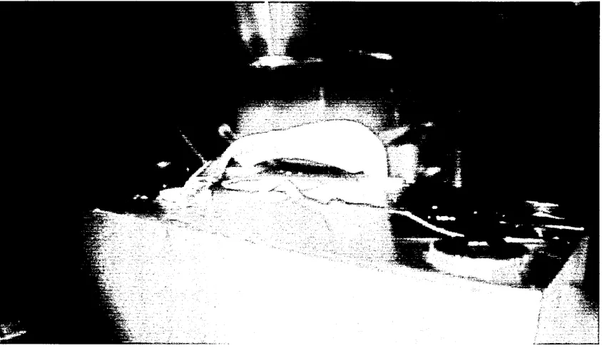
FIG 1. Henry Clifton Sorby, gentleman scientist. Sorby came from a respected Sheffield family, several of whom had been elected Master Cutler. He devoted his life to science in various forms, pioneering the use of microscopy first in geology, then in metallurgy and finally brought his energy to bear on research in natural history/biology and the promotion of scientific/technical education. Pictured aboard his yacht-cum-research vessel.
Mankind became aware of grain boundaries as an immediate and inevitable conse quence of Sorby’s invention of metallography. However, while grain boundaries were the first lattice defect to be observed, they are far more complex than point defects, dislocations or stacking faults, and will be the last lattice defect to be fully under stood. The scientific study of grain boundaries and their motion was started by C. S. Smith about the time of the Second World War; he divided the field into two sub fields, recrystallisation and grain boundary motion (grain growth) and pointed out the importance of grain shape.
FIG 2. Cyril Stanley Smith, Director of the Institute for the Study of Metals at University of Chicago. This was a de-militarised spin-off/continuation of the “University of Chicago Met Lab." project, which built the first nuclear reactor and produced the fissile metals for “The Manhattan Project”. Smith is shown holding a glass capsule full of soap bubbles - an early analogue/model of metal grain growth.
the production and preparation of the fissile metals required. On his return to a civil ian career, he appears to have had an intense interest in grain boundaries and some knowledge of the subject. These facts strongly suggest that the effectiveness of the most fearsome weapons of our time depend just as much on the control of their metal’s microstructure as did the effectiveness of the swords used by our ancestors.
The field of grain growth study was given added impetus by the work of E.O. Hall (1951) and N.J Petch (1953). Hall and Petch independently demonstrated the first quantitative relationships between grain size and strength, Hall in ductile yield of steel and Petch in brittle cleavage fracture of steel. The relations were then combined as follows:
, kH kp k
,7',r=a+7d
(HaN)
‘7c_<7°
7f
(Petch) a'I=a'0+Jd
(Hall-Petch)where cr,yp is lower yield point strength, ctc is brittle cleavage fracture strength, uy is yield strength, a* is the yield strength of a single crystal, <j0. kH, kp and K are con stants, d is mean grain diameter and I is mean linear intercept (proportional to d). ct0 is the “friction stress” or “dislocation friction" - increasing this term by alloying, second phases, precipitates, lattice distortion or creation of dislocation pile-ups is the other means of increasing material strength.
The Hall-Petch relationship was initially shown to be valid only for quite a narrow range of grain sizes, and only in steel, but was later shown to be valid in many other metals and shown to be valid over the full range of grain sizes in steel by W.B. Morrison (1966). This firmly established grain refinement not only as an important factor in commercial metals production, but also as a key research target for bringing improvement in materials technology.
2.2 MOTION OF GRAIN BOUNDARIES
2.2.1 FACTORS CONTROLLING GRAIN BOUNDARY MOVEMENT
It is now well known that grains grow in order to reach a low-energy equilibrium state, just as any other system in nature will develop towards the lowest feasible ener gy state. The balance between the surface energy and other energies associated with grain boundaries (e.g. mis-orientation energy, entropy) and the energy of the crystalline grain interior is such that the lowest energy state of a 3D grain network will be attained by the minimum number of grains. This implies maximum grain size, or minimum grain boundary area per unit volume, and that the shape of those grains should tend towards spherical. Clearly spherical grains imply small grains in the interstices, a situation that is not energetically favourable or implies gaps at the interstices, a situation that doesnot fulfil the topological space-filling requirements o f the grain network. Grains will grow and consume neighbouring grains in order to reach the stable low energy ideal, which is in practice attained with large grains each being (in 2 Dimensional section) hexagonal, i.e. with six nearest neighbours and in 3-D taking a form close to the “ Kelvin tetrakaidecahedron”, a curved face polygon whose closest plane-faced relative is the truncated octahedron, and having 1 4 nearest neighbours (Fig 3).
FIG 3.
The Truncated Octahedron and its thre-dimensional tessellation.
Image from http://en.wikipedia.org/wiki/Truncated_octahedron Last accessed 11/06/05
The surface energy effect, normally referred to as surface tension, is the main driving force behind grain boundary motion. Indeed, in most laboratory cases it is the only driving force. In industrial metals processing, the metal is likely to be under stress or to have been deformed very recently. Thus, in industrial situations, externally applied and/or as-yet-unrelaxed internal stresses, along with distortions to non-equilibrium grain shapes/boundary curvatures and junction angles, would be expected to be sig nificant additional drivers of boundary movement.
Opposing the net driving force are a large number of factors, many of which may interact. Mattisen et al. (2001) showed that at lower temperatures the m obility of triple junctions was lower than that of plane grain boundaries, and thus that grain boundary motion is retarded by the triple junctions present in the network. This w ork also showed boundaries and a triple point migrating at a steady rate in a high-purity aluminium tri-crystal. Estrin (2001) has shown that vacancies are generated in the freshly formed crystal left behind a moving grain boundary. These inevitably increase the energy of the freshly-formed crystal relative to the grain boundary energy, and thus would be expected to oppose the driving force by reducing the energetic “pay-back” o f eliminating grain boundary area.
There is much work showing that the presence o f solutes and/or segregates affects boundary motion, even at exceptionally low overall concentrations. Usually the effect is to retard motion, but occasionally motion is accelerated by the presence o f im
ties. However, the effect appears to depend upon many factors, such as velocity of boundary motion, temperature and the nature of the boundary and/or solute (Molodov et al, 1998). No clear pattern has yet emerged from this work. The effect of coherent and incoherent second phases or precipitates on boundary movement, Zener pinning or Zener drag (Zener 1948), is probably the most thoroughly investigat ed of the mechanisms of grain boundary retardation, and the most widely used means of grain refinement in industry.
2.2.2 THE NATURE OF GRAIN BOUNDARIES
To fully understand how some of these driving forces and retardation mechanisms might affect boundary motion would require a fairly detailed knowledge of the struc ture of grain boundaries. However, as Humphreys and Hatherley point out in their book (1995) "...there is still a great deal of uncertainty about the structure and properties of boundaries. Most of the theoretical and experimental work has been carried out for static boundaries and there is even more uncertainty over the structure, properties and energy of migrating boundaries, which are unlikely to be similar [to static boundaries]." Thus, it would appear unproductive to discuss the nature of boundaries in great detail here. It is proposed merely to outline the three main classes of boundary, namely low-angle, high-angle, and special.
Boundaries are described primarily by their angle, the minimum angle through which one crystal would have to be rotated in order to become continuous with the other, and if more detail is required, the crystallographic direction of the axis of that rotation is added. Special boundaries are also frequently described in terms of “Sigma” values, which correspond to certain specific misorientations. Due to the symmetry of cubic crystals the range of misorientation angles is limited, the maximum possible misorien- tation is 62.8° about <1,1, ((V2)-1)>, (i.e. 62.8° about <1,1,0.4142>). Values high er than this would be meaningless, as symmetry dictates that there would be a small er angle rotation available about some other functionally identical axis.
Low-angle grain boundaries (LAGB) are largely self explanatory and are roughly defined as those having a misorientation of 10-15 degrees or less, i.e. boundaries in which the interface can be formed from simple, though large, arrays of dislocations and whose nature is thus dependant on the size of the misorientation angle,
(Brandon, 1966). These low-angle boundaries are sometimes regarded as sub-grain boundaries, rather than “proper” grain boundaries and the behaviour of these bound aries (along with subgrain nucleation) are the main determinants of primary recrystalli sation behaviour. High angle grain boundaries (HAGB) generally have properties and structures that are largely independent of their misorientation angle, the exception
being special grain boundaries, a subset o f HAGB that do have structure and proper ties particular to their misorientation angle. Non-special HAGBs are often referred to as “random boundaries”.
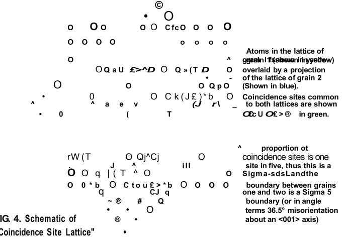
Special HAGBs, “CSL’ boundaries or “high-sigma” boundaries are those which possess a “coincidence site lattice” (CSL), originally proposed by Kronberg and Wilson in 1949. The coincidence site lattice concept is discussed at length in Randle’s books (1993,
1996). In a CSL boundary, if one lattice is notionally projected into the other, some proportion of lattice sites in one lattice coincide with the notional sites o f the other [fig 4]. Logically, this type of boundary has significantly less “free volum e” at the inter face than the “random” HAGB.
Free volume is the em pty space between the mis-matched neighbouring lattices, in which segregate or im purity atoms can easily congregate. The interstices between the atoms o f the main crystal lattice are only able to accommodate small atoms (e.g. car bon, nitrogen). Larger im purity atoms must either take the place o f an atom in the lattice (“substitutional” alloying) or congregate (“segregate”) in the grain boundary free volume, where there is space to accommodate them.
©
• O
O O O O O C fcO O O O O O O O o o o o
O ^ gram I fsnown in yenow
O Q a U £>^D O Q » ( T D O overlaid by a projection • - of the lattice of grain 2
O O O Q p O (Shown in blue).
• 0 O C k ( J £ ) * b O Coincidence sites common ^ ^ a e v (J r\ _ to both lattices are shown
• 0 ( T OCfc U O £ > ® in green.
^ proportion ot
rW (T O Qj^Cj O coincidence sites is one
. J ^ ill site in five, thus this is a
O O q | ( T ^ O O Sigma-sdsLandthe
O 0 * b O C t o u £ > * b O O O O boundary between grains
q CJ q one and two is a Sigma 5
~ ® # Q boundary (or in angle
[image:18.612.123.464.334.572.2]• • O terms 36.5° misorientation
FIG. 4. Schematic of ® • about an <001> axis)
"Coincidence Site Lattice" •
The “goodness o f fit” between the tw o lattices is expressed as the sigma value (a con cept proposed by Aust & Rutter in 1959), 2 being the reciprocal o f the proportion of sites coinciding. Thus 23 is a close coincidence w ith one in three sites common to both lattices, while 229 has just one in twenty-nine of its sites coincident. A coinci dence of sites is similar to the situation that would be found in a twin boundary, but these boundaries are assumed to have been formed conventionally and have migrated conventionally rather than forming by shear/distortion of an existing crystal. Therefore, special boundaries meet at a distinct boundary where all atoms, or at least most atoms,
are clearly allied to one crystal or the other, rather than both crystallites sharing a plane of atoms common to both, as in a twin. Unlike a twin boundary, there is free volume at a high-2 CSL boundary, but less than at random boundaries. They would thus be expected to have significantly different physics and segregate chemistry and thus different properties when compared to both twin boundaries and the other classes of grain boundaries. The importance of the sigma value is assumed to be 1) that it gives some guide to the free volume at the interface and 2) the fact that when the boundary moves, a significant proportion of the atoms can “move” from one crys tal to the other simply by changing their bonding allegiance, and without actually hav ing to physically relocate in space. Thus high-2 boundaries are expected to require less energy for grain boundary motion, or in other words to have a higher “mobility” - more movement for a given driving force.
Thus, it seems reasonable to expect three classes of behaviour from grain boundaries, corresponding to the three classes of boundary. There is much work to suggest that special boundaries, and certain low 2 values in particular, are more mobile than others as they tend to predominate in microstructures after certain more strenuous thermo mechanical treatment regimes. For example, as shown by Aust & Rutter (1959), Randle (1996) and Molodov (2001). This predominance of high-2 boundaries and the techniques for bringing it about are the basis of “Grain Boundary Engineering”. There is also much work that suggests that low angle grain boundaries, often regarded as sub-grain boundaries, are also more mobile than the “average". However, moving sub grain boundaries are principally associated with primary (initial) recrystallisation phe nomena, rather than grain growth, and have not been investigated in this work.
In summary, it appears that the motion of any particular grain boundary potentially depends upon all of the following:
♦ Surface tension driving force, dependant upon: • Local grain boundary curvature
• Grain radius • Grain shape
• Co-ordination (number of nearest neighbours)
• The balance of volumetric free energy -vs.- surface/boundary energy • Junction angles
♦ Opposing forces/factors, including: • Vacancy generation (Estrin, 2001) • Solute effects
• Triple junction drag (Shvindlerman et al. 2001, Mattisen et al, 2001) • Material diffusion across the boundary (matrix and impurity)
• Misorientation angle • Misorientation axis
• Velocity of boundary motion (instantaneous velocity) • Temperature
• Surface interactions (Humphreys et al, 1996) • Surface grooving (Mullins, 1958)
• Activation energy for motion • Precipitates (Zener Pinning) • Second phases
• Inclusions
• Interaction with dislocations (Molodov, 2001) ♦ Stresses
• Applied stresses (Winning, 2001) • Residual stresses
Clearly, many of these factors are likely to interact with others. For example, the intro duction of a segregate to a grain boundary would be expected to interfere with the transport of atoms across the boundary, but equally would be expected to alter the boundary surface energy - these could have synergistic or opposing effects. The exact behaviour of that segregate and the quantity that could segregate to the boundary would depend on the boundary free volume. The velocity of a boundary’s motion will affect the amount of segregate that it can sweep with it, which would in turn be expect ed to affect boundary velocity. A change in misorientation will change a boundary’s acti vation energy for movement, interaction with dislocations, thermal response, solute and segregate interactions and the boundary free volume (which might be expected to affect diffusion across the boundary and vacancy generation when in motion).
Logically, a high free volume boundary and/or a high velocity of motion, implies a rela tively long journey for atoms moving across from one crystal to the other. This implies a higher probability that any given atom will fail to reach its “ideal” lattice site before the grain boundary as a whole moves on, leading to the generation and “freezing-in” of vacancies, as observed by Estrin.
The forces and factors opposing grain boundary motion are often lumped together under the heading “grain boundary mobility” - the response of a particular grain bound ary to a particular driving force or surface tension. The term “mobility" to describe the
response of a boundary to a driving force is potentially misleading, as the phrase “high-mobility boundaries” evokes images of a class of boundaries moving much more rapidly than the rest. In fact, the high-mobility boundaries merely have the potential to move faster, if they are subject to the same driving force. Given the particular nature of high-2 boundaries, this is a big assumption. It is quite possible that the surface energy liberated by the elimination of a given area of high-2 boundary surface will be very different to that liberated by the elimination of the same area of random bound ary. Logically it would be expected to be considerably smaller, given the reduced free volume and the coincidence of lattice sites. Thus it is probable that a high-2 boundary will experience a different, and probably lower, surface-vs.-volume free energy balance component of the driving force, than would a random boundary under otherwise identical circumstances. It is therefore a dangerous assumption that “high-mobility” boundaries will necessarily move more rapidly in practice than will other boundaries.
In short, grain boundary motion is a complex phenomenon with a great many vari ables. some of which clearly are. and more of which may well be, inter-dependent. It is quite conceivable that conventional statistical techniques will prove to be of limited use in characterising grain boundary behaviour and that tools intended for “complex” or “chaotic” systems may be more successful if sufficient experimental data can be generated. Similarly, conventional experimental design is poorly equipped to cope with multiple inter-dependent variables, and a "Taguchi” experimental design scheme may prove more rewarding (Taguchi, 1987(1976)). The rather limited insight arising from the data currently available certainly implies that the problem is complex and resistant to analysis as well as lacking in experimental results.
2.2.3 INVESTIGATION OF MIGRATING BOUNDARIES
Due to the difficulties of working with materials at elevated temperature, the vast majority of the existing experimental work is based upon before-and-after studies, in which a grain structure is characterised, heated above its recrystallisation temperature for some time, then cooled and characterised again. Clearly, these “post-mortem” studies are generally unable to yield much meaningful information about the dynamics of grain boundaries (there are two specialised exceptions to this, i.e. the revealing of “ghost lines” by atomic force microscopy and segregate analysis). These before-and- after studies have reached only rather general conclusions about average grain sizes, a
fact that adds weight to the suspicion that the motion of grain boundaries is a com plex phenomenon that will not yield its secrets to such investigation techniques. Confusingly, many workers describe post-mortem experiments as “in-situ” if the sam ple area is rigorously controlled to be identical both before and after heating. For example, an experiment that images or maps the grains, then withdraws and/or
shields the detector while the sample is heated in place, then reintroduces the detec tor when the sample is once again cold may be referred to as “in-situ", but is clearly not the in-situ, in-real-time goal of this project.
There have been very few real time in-situ studies or studies with capability to detect or infer the position of a grain boundary at any point in time other than the beginning or end of the experimental run. With regard to “true” in-situ studies, Rabkin (2000), notes “The experimental observations in this field are scarce”and offers only two refer ences, Abdou et al (1996) and Molodov et al. (1998). Rost et al. (2003) (working on grain growth in thin films) further comment that In situ bulk observation of the evolu tion (grain growth) of polycrystalline mefo/s, especially during heat treatment proves to be difficult.”.They cite Van Swygenhoven (2002) and Marguiles et al. (2001).
Those few experimental observations that are available divide broadly into three types: those that show discontinuous “jerky” boundary movement, those that show steady, continuous motion and those that either do not state any observed mode of motion or have insufficient time resolution to conclusively show either of the first two cases. The first are typified by Rabkin et al. (2000). and Abdou et al. (1996). The second
type are typified by the work of Gottstein’s Aachen group: Mattisen et al. (2001), Gottstein et al., (2001). A third group (e.g. Humphreys et al, 1996) give images of grain networks at various times but do not report the mode of boundary motion. Regrettably Abdou’s most intriguing references are respectively “P.F. Schmidt, PhD the sis, University of Munster (1977)”, “TH Chuang, unpublished work (1985)” and “G. Kiessler, unpublished work (1986)”, none of which could be meaningfully consulted. In particular, Abdou et al. report that Schmidt's work showed discontinuous motion of a recrystallised grain growing into a copper single crystal matrix, with a maximum veloc ity about one order of magnitude higher than its average velocity. They also reproduce copies of two of Schmidt’s Time-Distance graphs. On-line searching for other relevant published articles by these authors has proved unproductive.
The data are very scarce, but it is notable that those workers finding jerky motion are mostly those working with polycrystals, while those that observe continuous motion are working with bi- and tri-crystals. Another interesting point is that Rabkin, observ ing an area covering a few grains, shows dwell times (the time during which an inter mittently mobile boundary remains stationary at any given position) in the order of minutes. By contrast, Abdou et al. (and some others cited by Abdou et al.) observe a small portion of a single grain boundary within a polycrystalline Rim and show dwell times in the order of seconds. These Rims are both artificially deposited thin Rims and Transmission Electron Microscope (TEM) specimens thinned down from bulk samples.
Much of the polycrystal research showing discontinuous motion has suffered from the fact that it is based on surface-imaging techniques. In all these cases, interaction with the specimen surface, and in particular with grain boundary grooves, will have influ enced boundary motion and has raised the suspicion, from some quarters of the research community, that this surface effect is sufficient in itself to account for the discontinuous motion observed. This may be particularly true with thin film and TEM studies, where surface effects would be proportionately much larger than bulk effects.
Since the start of this project, data has been published by Fielden et al. (2003), Schmidt et al. (2004), Juul-Jensen et al. (2004), Poulsen et al. (2004), Anselmino et al. (2004 A & B) and Fielden (2004). These show discontinuous motion at a surface in the absence of grain boundary grooves (Fielden, Anselmino et al.) and discontinuous vol ume changes and/or discontinuous boundary motion of a crystal within an aluminium bulk (Schmidt et al. Juul-Jensen et al. Poulsen et al. - the Riso laboratory 3DXRD group).
The surface results of Fielden and Fielden et al. (this project) and those of Anselmino et al. show discontinuous motion both before and after the appearance of surface groov ing. The in-bulk observations of the Riso group cannot be suspected of being subject to surface effects, but do suffer from very poor time resolution and the absence of any information on the context and/or neighbour grains of the growing grain/moving boundary. It is clear that discontinuous motion of grain boundaries in polycrystals occurs independent of interaction with the material surface. Most of these polycrystal studies use industrial materials, thus there still exists a possibility that ultra-high purity model materials may not exhibit discontinuous boundary motion in polycrystalline form, although Rabkin’s high-purity Ni-AI evidence suggests against this.
Until and unless the evidence becomes conclusive, the discontinuous motion results are likely to remain contentious, as the current models and theories of grain growth (Miodownik, 2002) envisage a near-constant surface tension driving force acting upon boundaries of near-constant mobility, i.e. a constant opposing force. While these forces will vary greatly from boundary to boundary, depending on boundary character, neigh bours, local topography, etc., for any given boundary moving from position A to posi tion B, with no other radical changes in neighbouring grain network geometry, these forces should remain roughly constant or should at least not change radically. This means that boundary velocity will change when local geometry changes, such as when a neighbour grain is annihilated, but that between such events boundary motion, while somewhat variable, should not be discontinuous or subject to large, sharp changes and boundary motion should neither stagnate permanently, halt temporarily nor fail to start.
2.3 INVESTIGATION TECHNIQUES CONSIDERED FOR,
OR SIGNIFICANT TO THIS PROJECT
The major techniques available to investigators are currently:
♦ Grain boundary etching/thermal etching techniques • Atomic Force Microscopy (AFM) techniques • Secondary electron SEM imaging
• Optical microscopy
♦ Post-mortem metallography of segregate distribution ♦ X-Ray diffraction techniques
• 3D-XRD microscopy (a synchrotron radiation X-Ray Diffraction technique) • X-Ray tracking of a single grain boundary
♦ Backscattered Electron techniques, composed of: • Electron imaging
• Orientation mapping (EBSD)
2.3.1 GRAIN BOUNDARY ETCHING/THERIVIAL ETCHING TECHNIQUES
These techniques rely upon the phenomenon of etching of grain boundaries. This induces a topographic feature on the specimen surface at the grain boundary position, thus allowing topographic imaging techniques such as optical microscopy, secondary electron scanning electron microscopy or atomic force microscopy to detect the boundaries indirectly, via the etched features.There are two means of etching, chemical and thermal. In chemical etching, material is removed from the specimen by exposing it to a moderately corrosive chemical mix, usually for a brief time. The etchant is carefully selected such that it will be incapable of significantly affecting the bulk of the crystal grains of the material, but will remove material from the grain boundary, which is more chemically active due to the disrupt ed crystal lattice that is the boundary. Electro-chemical or electrolytic etching can also be employed, but is functionally the same. Both techniques are widely used in con ventional optical metallography.
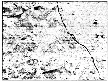
In thermal “etching” (or grain boundary ditching) [fig.5] no material is removed.
Material is transported by surface diffusion from the grain boundary and deposited on the adjacent surface of a grain. This process can only occur at temperatures relatively close to the melting point (Mullins, 1957).
Polished Surface
Diffusion
Grain
/
Boundary
FIG. 5. Formation of a grain boundary ditch by thermal etching (surface diffusion)
Grain
Boundary
The driving force for thermal etching is surface tension. A sharp corner on a grain (shown in the “as polished” case above) is energetically unfavourable - the “ideal” low- energy configuration for the triple junction between three grains is three angles of 120° each. The equilibrium angle between two grains and the surface will not be 120°, but is highly unlikely to be 180°, as in the “before” diagram o f fig 5. Thus, mate rial will diffuse away, bringing the surface-grain-grain junction angles closer to equilib rium, once the temperature becomes sufficient to activate surface diffusion in the material. This diffusion is time and temperature dependent.
2 .3 .1 .1 Lim it a t io n s o f Et c h in g Te c h n iq u e s
Because diffusion is time dependent, a ditch will not appear instantly when a grain boundary moves to a new position. Neither will an existing ditch disappear when the grain boundary that caused it moves away. Thus, if the boundaries are moving at any speed, thermal etching techniques could easily give a misleading impression o f the instantaneous position o f the boundaries.
With chemically etched specimens not only will the prior surface topography not van ish, but new topography will not appear at the new boundary positions until and unless the specimen is re-exposed to an etchant.
Finally, all techniques that induce surface topography will suffer from the suspicion that the topography generated will probably influence the motion o f grain boundaries that intersect the surface [Fig. 6] (Mullins, 1958).
Grain boundary, pinned Boundary moved, no groove at new position (yet)
FIG. G. Grain boundary pinned by surface groove, then breaking away
2.3.1.2
Op t ic a l Mic r o s c o p y a n d Se c o n d a r y El e c t r o n Te c h n iq u e sAs noted above, these techniques rely upon induced surface topography in order to indirectly detect the position of a grain boundary. There are however two “special cir cumstances” exceptions to this.
1) Zinc has optical properties which are anisotropic with crystal orientation, thus grains of zinc can be imaged optically without etching (e.g. Shvindlerman et al. 2001). Unfortunately, zinc has hexagonal close-packed crystallography, and may therefore reveal relatively little about the behaviour of the metals with face-cen tred cubic crystals that are this project’s primary focus.
2) Secondary electron emission from a specimen is generated by the passage of high-energy electrons either into or out of the specimen surface. Thus, a pro portion of the secondary electron signal corresponds to the backscattered elec trons leaving the specimen. If the (topography dependent) contrast in the beam- induced secondary signal is practically non-existent (high quality flat polished specimen) then a very weak contrast may be observed between crystals using secondary electron imaging. This is an indirect use of backscattered electron imaging, which is discussed in more detail in that section (2.3.3).
2.3.1.3
At o m ic Fo r c e Mic r o s c o p y t e c h n iq u e sAtomic force microscopy “images” surface topography by physically scanning it in a raster pattern with a nano-scale stylus, but in addition it measures the surface fea tures that it encounters, this technique has been used by Rabkin et al. (2000) and Rabkin & Klinger (2001) to investigate the movement of grain boundaries in a poly crystalline Ni-AI intermetallic compound at high temperature.
A knowledge of surface diffusion rates for the material of interest at the temperature of interest is necessary. Given this knowledge, and the depth of a grain boundary ditch as measured by the AFM, it is possible to calculate the time over which the ditch forming diffusion mechanism was in operation. This time will correspond to the time at temperature for a stationary grain boundary, or would be the time spent dwelling at a position for a mobile boundary. Rabkin’s work shows some grain boundaries remaining stationary throughout his experiment while others move in a discontinuous fashion, leaving behind them telltale trails of partially formed ditches or “ghost lines", indicating the positions at which the boundary stopped and the approximate duration of the stationary dwell.
2.3.1
A
T h e P o s t-m o rte m M e ta llo g r a p h y T e c h n iq u eRabkin (2001) refers in passing to ghost lines revealed by metallography and appropri ate etching to reveal segregates. Chongmo and Hillert (1982) used the technique to investigate diffusion induced boundary migration. Moving grain boundaries tend to sweep segregate, impurity or alloy elements with them, but. when moving rapidly, the quantity of segregate that can be carried is reduced. Thus, if a boundary moves in a dis continuous manner, segregates will be found at higher concentrations where the bound ary has stopped, as they were unable to follow the boundary when it re-commenced movement and accelerated away. The increased concentrations of segregates at these positions can be etched for and imaged. However, these are highly specialised and problematic techniques. Spatial resolution will be much reduced by the fact that, once free of the boundary, segregates will tend to diffuse away during the remainder of the heating time, “smearing” the position indication. This makes the segregate concentra tion more difficult to detect, and, in the case of brief dwells, erases the segregate con centration evidence by reducing it to a level indistinguishable from the background. No evidence was found in the literature for the use of this technique to study boundary motion in single-phase materials, however the technique is used to determine posi tions of prior austenite grain boundaries in cooled and transformed steel specimens.
Sensitive microanalysis techniques such as Secondary Ion Mass Spectroscopy (SIMS) have the potential to directly map segregate concentrations. However, no reference has been found to their use for this purpose, and they would be subject to many of the same problems.
2.3.2 X-RAY DIFFRACTION TECHNIQUES
These techniques rely on diffraction of X-Rays passing through the crystal lattice and either the disturbance of this diffraction by the grain boundary or the difference in diffraction generated by some differently oriented crystal. The simplest of these tech niques is grain boundary tracking by X-Ray.
2.3.2.1
Gr a in Bo u n d a r y Tr a c k in g b y X -Ra yIn this technique, an X-Ray beam is directed onto a polished specimen such that the diffraction process reflects the beam to a detector, as illustrated below [fig 7]. The intensity of the reflected beam will be different for the two differently oriented crys tals, and different again where the beam falls on the grain boundary and straddles the two crystals. By calibrating the system with the boundary reflection intensity, a logic controller can be set up to hunt for that intensity and thus track the position of the grain boundary. The system was developed by Gottstein’s Aachen group (Czubayko et al., 1995) and is heavily used by them.
FIG. 7. "XCITD" X-Ray Continuous Interface Tracking Device schematic
x
Signal
X-Ray
Source
-Ray
Detector
Moving grain
boundary
Logic
Controller
Control
Moving Table
The system that this author has seen maintains the X-Ray beam source and detector stationary and moves the specimen stage such as to keep the grain boundary at the point where the beam hits the specimen. Clearly the system is limited in that the stage is only capable of one dimensional movement, though 2-D motion is theoreti cally possible. Also the logic processing and X-Ray optics are greatly simplified by a knowledge of which direction the boundary will move in. Two dimensional motion could be tracked, but would probably entail a much reduced response time.
Current boundary tracking systems use artificial bi-crystals, and occasionally tri-crystals as specimens, and often apply a magnetic field to drive grain boundary motion, as the form of a bi-crystal dictates little or no surface tension driving force (Gottstein, 2001 B).
A further limitation is the fineness o f the X-Ray beam. If the technique were applied to a polycrystal, the beam would have to be small with respect to the grain size present in order to avoid detection o f more than one boundary simultaneously. Similarly the beam would have to be large with respect to the “X-Ray visible” boundary w idth, in order to produce a clear and repeatable target intensity. Given the technical difficulties o f producing finely collimated X-Ray beams o f relatively high intensity this technique seems likely to remain limited to studies o f model systems.
2.3.2.2 “3-D XRD” M ic r o s c o p y
3-D X-Ray Diffraction microscopy is an extremely expensive technique is based upon high power synchrotron X-Ray beams, the instrument is usually installed for just a few weeks o f the year at the E5RF (European Synchrotron Radiation Facility) at Grenoble or at DESY (Deutsches Electronen SYnchrotron) in Hamburg. A similar instrum ent is under development at Argonne National Laboratory, near Chicago in the USA.
A high-brightness X-ray beam, typically of2 40keV energy, is passed through a specimen and diffracted to an annular detector. A thick metal shielding mask is placed in front of the detector. This contains very narrow slots, machined and aligned in the form of part of a cone, such that only diffracted rays originating from a small target volume at the apex of the cone (the gauge volume) can pass through to the detector. This gauge volume is presently at best about 1 micron x 1 micron x 20 microns. The specimen is mounted on a 3-D movable stage, such that the gauge volume can effectively be scanned around the specimen’ s volume (actually the specimen is scanned through the gauge volume) and diffraction data is captured to form a 3-D map. Alternatively, the diffracted signal from one crystal can be monitored and the specimen either scanned, to build a 3D topography map of just that crystal or monitored for its intensity with the specimen stationary. This latter yields a measure of the volume of a grain, but not its shape, location or context (Juul-Jensen (2001), Lauridsen (2003), Poulsen et al. (2004)). The specimen can be heated, or strained during X-Ray examination. This sys tem was successfully used by Lauridsen et al (2001), to monitor the volume of a growing grain of known orientation in a bulk of 1050 Aluminium and later by Schmidt et al. (2004) to sequentially map the 3 dimensional shape of a growing grain over time. There are several major limitations to the technique:
♦ In order to monitor a particular grain it is necessary to forgo capturing any infor mation on its neighbours or the context surrounding it
♦ Spatial resolution is poor by comparison to most other techniques
♦ Time resolution is very poor, as each full volume scan takes a considerable time to complete, particularly if more than one crystal is being monitored or if crystal shape is being mapped rather than simple volume being monitored.
2.3.3 BACKSCATTERED ELECTRON TECHNIQUES
(INCLUDING “FORWARD” SCATTERED ELECTRONS)
These techniques rely upon two phenomena. Firstly, the partially directional scattering of backscattered electrons, a proportion of which are diffracted and/or channelled to form Kikuchi or Electron BackScatter Patterns (EB5P). Secondly, the small changes that occur in overall backscattered electron signal (i.e. changes in absorption or backscattering coefficient) with changing electron probe/crystal lattice geometries, due to channelling and consequent preferential absorption.
2 .3 .3 .1 Me c h a n is m s o f El e c t r o n Ba c k s c a t t e r in g
The electrons of the microscope beam (primary electrons) penetrate the specimen material (in the context of this project, a metal crystal). The electrons very rarely strike or interact with the surface atoms, but once inside the specimen, can interact with
the electrons and atoms of the material in a variety of ways and hence ultimately suf fer a variety of fates. The electrons of interest in the context of this project are among those that are “backscattered". In the near-surface bulk of the specimen, these elec trons undergo a number of elastic and/or inelastic collisions/interactions with atoms and their nuclei. Ultimately they escape from the material surface with a relatively large fraction of their initial energy remaining, albeit with the vector of their velocities deviated through a large angle. Most electron-specimen interactions can be relatively simply explained in terms of particle interactions (collisions) despite the fact that mov ing electrons have both wave character and particle character.
Backscattered electrons will have undergone one or more scattering encounters (pos sibly several) prior to exiting the specimen. These encounters will be a mixture of inelastic and elastic collisions, thus the exit energy of the electron will generally be inversely dependent upon the number of scattering encounters it has undergone, exit energy being lower if the number of collisions is high. Repeated collisions may send the electrons on a journey analogous to a 3-D random walk, biased by the uniform initial velocity of the electrons and the probability that the angle of scattering in any one encounter will be relatively low (see Reimer, chapter 3). By implication the lower energy backscattered electrons, having undergone a larger number of small-deviation collisions (i.e. having taken a longer random walk), are likely to exit the specimen fur ther from the beam entry point than will the Low-Loss backscattered Electrons (LLE). that have suffered one or very few large-deviation collisions, This accounts for the rel atively low resolution of backscattered electron imaging compared to the more fre quently used secondary electron imaging in conventional scanning electron
microscopy. Secondary electrons (which give higher resolution images) are ejected by the passage of the incident electrons (SE1 secondary electrons) and also by the pas sage of low-loss backscattered electrons exiting the specimen from a relatively com pact area around the beam entry point (SE2 secondary electrons). The higher-loss backscattered electrons exiting the specimen more distant from the beam entry point generate fewer SE2 electrons and thus make a progressively smaller contribution to the overall SE image. By contrast, the common backscatter electron detectors are designed to respond almost equally to backscattered electrons across a fairly wide range of energies, thus the high-loss BSE make a proportionally larger contribution to the image and limit the available resolution. For more detail on any of the foregoing, Reimer’s book (1998) is recommended.
By convention, “backscattered” electrons are defined as being those that escape the specimen with an energy in excess of 50 eV (from a primary beam energy of typically 20 KeV). This definition is convenient because it reflects the range of electron energies likely to be detected by “backscattered” and “secondary” electron detectors respective
ly. However, it is not wholly accurate, nor is it particularly convenient in the context of this project. As noted below, this broad definition of backscattered electrons includes “channelled” or diffracted low-loss electrons carrying valuable information on crystal structure as well as a large number of “ordinary” backscattered electrons, which can provide a strong and unhelpful background signal.
2 3 . 3 . 2 Im a g in g Cr y s ta ls v ia Ba c k s c a t t e r e d El e c t r o n s
Crystal Orientation Imaging/Electron Back-Scatter Diffraction (EBSD) mapping tech niques rely upon the fact that the intensity (number) of backscattered electrons arriv ing at any given point on some detector area (usually a phosphor screen) will vary with varying crystal orientations relative to the detector. This geometry dependent variation of intensity is due to channelling and/or diffraction of the electrons escaping from the specimen.
A proportion of the incident electrons, having been scattered by encounters with the specimen atoms/electrons, will ultimately be sufficiently deviated from their original direction as to be moving back towards the material surface. If the number of scatter ing interactions was low and/or their nature mostly elastic then the backscattered electron will retain a high fraction of its initial energy (have a short equivalent wave length) and thus may usefully interact with the specimen on its journey back to, and exit from, the (crystalline) material surface. The nature of these interactions can be simplistically explained by diffraction of the electrons, which have wave character, by the regular network of the crystal atoms. This model is analogous to the simplest models of transmission electron microscopy, the backscattered electrons appearing to come from some virtual electron source within the material, albeit a very poorly colli mated and polychromatic source.
The electron backscattering patterns are often referred to as “Kikuchi” patterns from the diffraction phenomenon that produces them. Some of the electrons travelling (in many directions) towards the surface will be diffracted by passing between the atoms of the lattice. Because the electrons are travelling in a variety of directions, the diffraction does not produce a spot pattern (as would be expected from a single beam), but a line pat tern resulting from conical families of diffracted beams. The lines from one diffraction are overlaid by the lines resulting from diffraction from the lattice’s other directions of symmetry, producing a characteristic pattern of lines and nodes [fig 8J on a screen [fig 9j. To maximise pattern clarity, the specimen is tilted at 70° to the beam in order to maximise backscattered electron yield and the centre of the detector/phosphor screen is similarly at 70° to the specimen (140° to the beam) to maximise electron capture.
Phosphor Screen
Camera
Fore-Scatter Detector
N r
Electron beam
Specimen
FIG. 8. A typical high-quality FIG. 9. Schematic of EBSD system Electron Back-Scatter Pattern.
More sophisticated models of this interaction consider the phenomenon of “Chan nelling", which is discussed further below. In summary, due to the regular stacking of the crystal lattice, there are certain directions in which it is easier for the electron to pass through the crystal (or put another way, directions in which the electron is likely to travel further before being deflected or absorbed).
This effectively increased “transparency” to electrons travelling in certain specific direc tions would account for some of the directional nature of backscattering and for ori entation-dependent preferential absorption of some incident electrons. For example, if the incident electrons happen to coincide with a channelling direction leading into the crystal they are likely to scatter at a greater depth and thus are less likely to exit the specimen before being absorbed. In a backscattered electron image, such a crys tallite would appear slightly darker than some randomly oriented crystallite.
Thus the journey of an electron [fig. 10], which was earlier referred to as analogous to a biased random walk could be better modelled as a three-dimensional game of snakes and ladders. Conventional electron-specimen collision interactions are the steps along the main random-walk path, but with the electron likely to lose energy at each collision the number of “dice-rolls” available to it is limited and only those few that roll consistently high will reach the end of the game and exit the surface. Most will run out of energy and be absorbed. However, a proportion will encounter a chan nel - a snake or a ladder - moving the electron a relatively great distance, perhaps even to the surface, for little or no energy loss. Not all channels lead to the surface. Like the snakes in the game, some channels lead even deeper into the specimen, from where the electron is even less likely to escape.
Vacuum
Specimen
FIG. 10. A typical "Monte Carlo" simulation of electron-specimen interaction
The diffracted and/or channelled backscattered electrons leave the specimen in fam i lies of preferred directions. The conventionally backscattered electrons are em itted in a much more nearly omni-directional fashion and may well have lower energies (as channelled electrons have effectively taken a “short cut"), although the overlap is large. These conventional backscattered electrons provide a large background signal, which degrades the contrast that ought to be available in the diffracted/channelled portion of the low-loss backscatter signal (which carries the orientation inform ation).
Electron Backscatter Diffraction (EBSD) captures a large portion o f the structured back scatter pattern across a large detector area [fig 9] and exploits image processing and computing technology to determine what crystal orientation is most likely to be respon sible for producing the observed pattern (Randle’s book, 1993, gives a good overview).
2 .3 .3 .3 Or ie n t a t io n Co n t r a s t Im a g in g
Orientation Contrast Backscattered/fore-scattered electron imaging follows one of two possible strategies.
The more common approach, often referred to as “ forward scatter electron imaging” , or “fore-scatter imaging” is usually done in the same “ forward scatter” geom etry used by EBSD and is often carried out in conjunction with EBSD [fig 9], This captures a backscattered electron flux falling on one or more relatively small detectors, and gen erates image contrast from the geom etry dependent changes in that flux, i.e. changes in the diffracted/channelled contribution (dependent upon detector-crystal geom etry).
The detector lies in a small part of the electron backscatter pattern cast by the subject crystal, and as the pattern will change when the beam moves on to a differently ori ented crystal, the flux falling on the detector is likely to change as well. However, as this change is likely to be very subtle, fore-scatter detectors are often deployed in arrays of up to six elements, with sum or difference signal imaging options in order to enhance contrast for any given specimen. A further problem with detectors deployed with an EBSD system is that the ideal location for detectors (70° to the specimen,
140° to the beam) is already occupied by the EBSD detector screen, and thus the fore-scatter detectors are usually at a very oblique angle to the specimen, nearly 90°. This reduces the signal strength and greatly exaggerates topographic contrast. Even in “flat polished specimens”, such as those produced by electropolishing, the greatly exaggerated topography contrast can easily overwhelm or mask the orientation con trast (Seward 2003, Reimer 1998 p 224).
The less common approach, usually referred to as Electron-Channelling Contrast Imaging (ECCI) or simply as Orientation Contrast (OC), can be done at the 70° posi tion and the zero-tilt position. It employs a large detector area, capturing an averaged signal to detect changes in overall backscattered electron flux, i.e. changes in back- scattering coefficient, T], due to the differential absorption due to channelling (depend
ent upon beam-crystal geometry), see Simkin 2001. The set up used for this imaging mode is identical to that used for producing channelling patterns in the SEM, however it is unnecessary to rock the beam, as the desired beam/crystal angle changes are pro vided naturally by multiple differently oriented crystallites.
Backscattered Electron imaging techniques are limited by the detectors available and the low contrast/weak signal both of electrons backscattered to form a channelling or Kikuchi pattern and of the generally very small differences in backscatter co-efficient between crystals oriented for maximum channelling compared to those oriented for minimum channelling. This latter contrast, the maximum ratio of Ati/t], is shown by
Reimer (p358 and fig 9.17) to be in the order of 1 -5%, for most materials.
2.3.3.4i
Ba c k s c a t t e r e d e l e c t r o n d e t e c t o r t e c h n o l o g yThere are currently two major classes of readily available detector for backscattered electron imaging: semi-conductor diode detectors and scintillation detectors (based on the Everhart-Thornley secondary electron detector, including the Robinson detec tor). Also available are microchannel plate detectors, these tend to be restricted to specialised low beam energy applications and are very expensive. The diode detector is by far the most common of these types, and all of the recent published data on SEM imaging of grain structures appears to have been generated by workers using diode detectors. The limitations of the various detectors are discussed below.
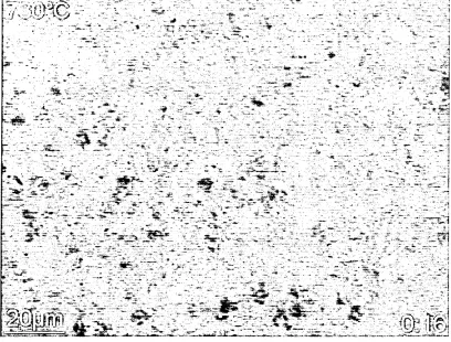
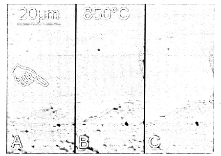
2.3.3.4.1 Limitations of Techniques Based on Diode Detectors
The Diode detectors are sensitive to light and Infra-Red (IR) photons, one or both of which will be emitted from any hot specimen - depending upon just how hot it is. This is an extremely serious limitation, as both the industrial and model materials of most interest for investigation undergo grain growth at relatively high temperatures, at which significant photon fluxes will be emitted. For example: aluminium - in the order of 300°C and upwards, steels in the order of 700°C upwards, gold & copper in the order of 500°C and upwards. Signal contrast from the detector decreases as photon radiation increases until the point where the major workers using this technique report that there is no usable image contrast when specimen temperature exceeds about 400°C or 450°C (Humphreys, 2001: Mattisen 2001). Attempts have been made to screen the detectors from the hot sample and stage, however as both the undesired photons and the desired backscattered electrons follow line-of-sight paths, success has necessarily been limited (Anselmino (2005), Mattisen (2001)). Both Anselmino and Mattisen’s information is with regard to partially successful screening by apertures and shields to restrict the IR reaching the detector to only that which emanates from the area of interest, not the rest of the sample or the hot stage as a