http://wrap.warwick.ac.uk
Original citation:
Núñez, C., Domínguez-Adame, F., Orellana, P. A., Rosales, L. and Roemer, Rudolf A.. (2016) Silicene-based spin-filter device : impact of random vacancies. 2D Materials, 3 (2).
Permanent WRAP url:
http://wrap.warwick.ac.uk/73861
Copyright and reuse:
The Warwick Research Archive Portal (WRAP) makes this work by researchers of the University of Warwick available open access under the following conditions. Copyright © and all moral rights to the version of the paper presented here belong to the individual author(s) and/or other copyright owners. To the extent reasonable and practicable the material made available in WRAP has been checked for eligibility before being made available.
Copies of full items can be used for personal research or study, educational, or not-for profit purposes without prior permission or charge. Provided that the authors, title and full bibliographic details are credited, a hyperlink and/or URL is given for the original metadata page and the content is not changed in any way.
Publisher’s statement:
Published version: http://dx.doi.org/10.1088/2053-1583/3/2/025006
A note on versions:
vacancies
C. N´u˜nez1,3, F. Dom´ınguez-Adame2,3, P. A. Orellana1, L. Rosales1, R. A. R¨omer3
1Departamento de F´ısica, Universidad T´ecnica Federico Santa Mar´ıa, Casilla 110 V,
Valpara´ıso, Chile
2GISC, Departamento de F´ısica de Materiales, Universidad Complutense, E-28040
Madrid, Spain
3Department of Physics and Centre for Scientific Computing, University of Warwick,
Coventry, CV4 7AL, United Kingdom
E-mail: [email protected]
l
Abstract.
We propose a hybrid spin-filter device based on a silicene nanoribbon. A ferroelectric polymer grown on top of the nanoribbon splits spin-up and spin-down electron bands and gives rise to a spin polarisation of the conductance. In particular, we study the effects of a random distribution of vacancies on the performance of this spin-filter device. Disorder induces Anderson localisation of electrons and we find that the localisation length strongly depends on the electron spin. By adjusting the Fermi level of the source contact, only electrons with one spin orientation can reach the drain contact because their localisation length is larger than the length of the device. Electrons with opposite spin are largely back-reflected. Electric conductance then becomes spin polarised and the device behaves as a quasi-half-metal. We conclude that a moderate concentration of vacancies has little impact on the spin-filter capabilities of the device, opening the possibility to using it as a tuneable source of polarised electrons.
PACS numbers: 72.25.Dc 72.80.Ng 73.20.At
1. Introduction
Silicene is the silicon analogue of graphene [1]. These two-dimensional materials share a common honeycomb lattice structure [2–4] but the larger ionic radius of silicon induces a buckling of the lattice [2, 4]. The two sublattices of the honeycomb lattice are hence not coplanar in silicene and first-principles calculations suggest that the spin-orbit interaction opens a sizable gap at the Dirac point of the order of 1.55 meV [5]. Due to the relatively large spin-orbit interaction, silicene is thought to be an ideal candidate to observe the quantum spin-Hall effect at realistic temperatures [6]. Remarkably, the buckled structure of silicene allows the magnitude of the gap to be controlled by applying a perpendicular electric field [7]. The band gap as a function of the electric field presents a characteristic W-profile and closes at a critical magnitude of the field [7]. The topological phase transition that occurs at the closure is characterized by an inversion/crossing behaviour of the R´enyi-Wehrl entropy of electrons and holes [8]. The interest in artificially synthesized silicene as a material of choice for nanoelectronics [9] is motivated by the inherent difficulty of opening an electronic gap in graphene. Silicene could in principle offer an alternative to overcome this limitation found in graphene because its buckled structure favours opening a gap that can be additionally controlled by an electric field. In this context, Taoet al. recently reported the fabrication of a single-layer silicene field-effect transistor that operates at room temperature [10]. Furthermore, the topological phase transition can be exploited to alter charge transport in np and nnjunctions of silicene by a side-gate voltage [11].
Spin-related and magnetic effects are of special interest for their relevance in spintronics. Hybrid nanostructures containing EuO ferromagnetic insulator layers deposited on top of graphene quantum rings [12, 13] and superlattices [14, 15] provide a route to design spin-filters and spin-valves. The ferromagnetic layers induce a proximity exchange splitting of the electronic states in graphene [16, 17], resulting in the appearance of a spin-dependent potential profile. The electric current through the hybrid nanostructure can be highly polarised and gives rise to spin-dependent negative differential resistance [14, 15]. It should be mentioned that the level splitting due to the proximity exchange interaction with the Eu2+ ions is relatively small, of the order of 10 meV. Better performance could be achieved by using ferroelectric polymers because it is believed that they induce an energy shift of the spin-up and spin-downs bands of the order of 0.5 eV [18]. Regarding the combination of silicene and EuO in the design of hybrid devices, Wang et al.[19] investigated electron transport in those systems and concluded that they could be a perfect spin and/or valley half metal by controlling the external electric field and the magnetisation.
of intentional or unintentional disorder on the transport properties of the proposed device. To do so, we have considered a random distribution of vacancies which localises the electrons in the nanoribbon, due to the appearance of Anderson localisation [20]. Our results demonstrate that the localisation length strongly depends on the electron spin. By setting the Fermi level and the other parameters of the device, most electrons with one spin orientation can reach the drain contact because their localisation length is larger than the length of the device, but electrons with the other orientation are largely back-reflected. Hence the electrical current can be highly spin-polarised and the system behaves as a quasi-half-metal, as a result of the coexistence of both metallic and insulating nature for electrons with different spin.
2. Theoretical model
[image:4.612.143.450.453.568.2]The proposed system consists of a rectangular silicene nanoribbon of width W and length L connected to source and drain leads, as shown schematically in figure 1. In order to avoid topologically protected edge states that appear at the Fermi energy in zig-zag nanoribbons we restrict ourselves to nanoribbons with armchair edges hereafter. It worth noticing that a similar trend is expected in gapped zig-zag nanoribbons. A ferroelectric polymer grown on top (or, equivalently, below) induces a spin-splitting of the electronic states in the silicene nanoribbon. Consequently, a spin-up (spin-down) electron propagating along the sample will be subjected to a positive (negative) constant potential.
Figure 1. Schematic view of the device. The armchair silicene nanoribbon is connected to left (L) and right (R) leads, with a ferroelectric polymer grown below it (blue shade). Lattice distortion around vacant sites is neglected. In our model, vacancies are described as sites whose energy is very large compared with the silicene bandwidth.
Electrons in the bipartite silicene honeycomb lattice are described using a single
π-orbital tight-binding Hamiltonian [7],
H =−t X
hi,jiσ
c†iσcjσ+ i λSO 3√3
X
hhi,jiiσβ νijc
†
iσσzcjβ+
X
iσ
c†iσ(M σz+εi)ciσ , (1)
are indicated by σ and β hereafter. The first term of the Hamiltonian (1) corresponds to nearest-neighbour hopping with energy t = 1.6 eV [7]. The second term represents the spin-orbit coupling with λSO = 3.9 meV, where νij =±1 is the Haldane factor [21]
and σz is the Pauli spin matrix. Finally, the third term takes into account the
spin-splittingM of electron states due to the interaction with the ferroelectric polymer. For simplicity we assume that the spin-splitting is the same in both sublattices. Vacancy disorder is described by a random site energy εi. We choose it to take on very large
values, εi = 103t, with concentration probability c. For non-vacant silicence sites, we
have εi = 0. Therefore we identify the vacancy concentration c with the fraction of
vacant sites in an otherwise regular silicene honeycomb lattice. We neglect possible lattice distortions around vacant sites since these will not qualitatively affect the results. We study electron transport across the nanoribbon using the Green’s function formalism combined with decimation techniques [22]. In the linear response regime, the conductance is calculated from the Landauer formula [23]. In terms of a single particle Green’s function, the conductance is then given as [24]
Gσ(E) =G0 Tr h
ΓL(E)G
†
SN(E)ΓR(E)GSN(E)
i
σ , σ=↑,↓ , (2)
where G0 = e2/h is the quantum of conductance per spin. Here the functions
Γα(E) = i
h
Σα(E)−Σ†α(E)
i
with α = L, R describe the spin-independent coupling between the nanoribbon and the left (L) and right (R) contacts, and Σα is the
spin-independent self-energy of each lead. They are defined as Σα(E) = VC,αgα(E)Vα,C.
Here, VC,α are the tunnel coupling matrix elements and gα(E) is the surface Green’s
function of the corresponding lead. The Green’s function GSN(E) of the silicene
nanoribbon is determined from the equation GSN(E) = [E−H−ΣL(E)−ΣR(E)]
−1
, with H as given in (1).
The dimensionless weighted polarisation of the spin-dependent conductance is defined as
Pσ = G↑(E)−G↓(E)
G↑(E) +G↓(E)
Gσ(E)
G0
, σ =↑,↓, (3)
and it will be the figure of merit to assess the spin filtering properties of the device. The dimensionless weighting factor Gσ(E)/G0 is introduced to get rid of small values
of both G↑(E) and G↓(E) that could lead to anomalously large values of the quotient [G↑(E)−G↓(E)]/[G↑(E) +G↓(E)].
3. Results
the safe side. Higher values would result in better performance of the device, as we will discuss later. Moreover, different imperfections or perturbations, in particular disorder, can affect the conductance and its polarisation in non-ideal samples. There are various possible sources of disorder, for example, charged impurities in the substrate or point defects like vacancies. While the former would provide some additional smooth electrostatic potential and can hardly deteriorate the transmission through the device to a large extent, the impact of the latter on the transport properties is probably stronger, especially for small devices. In order to estimate the impact, we will simulate samples with different vacancy concentration, from c = 0 (clean sample) up to c = 0.1. This results in a spin-dependent random potential that yields different localisation length for spin-up and spin-down electrons at the Fermi level.
In figure 2(a) we show the resulting spin-dependent conductance Gσ (σ =↑,↓) as
a function of energy E for both spin directions. In our simulations we set the width of the nanoribbons as W = 2.35 nm and their length as L = 23.22 nm, unless stated otherwise. Results of the clean sample are compared to the averages over 100 realisations of random samples with c= 0.01. The shape of the conductance curve is essentially the same in both spin orientations but shifted by an amount 2M. An overall decrease of the conductance arises when a random distribution of vacancies is present in the nanoribbon. We observe a marked reduction of the conductance around the band centre (E = 0 eV) on increasing vacancy concentration while retaining relatively high values at the edge of the first mode energy window (|E| ∼ 1.0 eV). We will show later that the decrease is caused by a destructive interference pattern in the disordered potential landscape, namely Anderson localisation [20]. We can then take advantage of the abrupt profile of the conductance curves to induce quasi-half-metallicity in the sample, as shown in figure 2(b). When the Fermi level lies in the range between 0.75 eV and 1.15 eV, the difference between spin-up and spin-down conductances is maximal (about a quantum of conductance per spinG0). Under these conditions, electric current will be strongly
spin-polarised. Most importantly, Anderson localization induced by the random distribution of vacancies leads to a nonuniform decrease of the conductance and it is less pronounced around E = 0.85−0.95 eV. The corresponding polarisation for both spin directions is similar to that shown by the clean sample [see shaded area in figure 2(b)]. In this energy window the degradation of the spin polarisation as a consequence of disorder is negligible when c = 0.01. We also observe a narrow dip at E ∼ 0.95 eV with large
P↓ ' −1.5 in the clean sample and P↓ ' −1.0 in the disordered one. However, the dip is very narrow (0.01 eV) and would be smeared out at temperatures above 120 K. In addition, the polarisation is significantly reduced in this energy window in the presence of disorder. For these reasons, we belief that the narrow dip is not of interest for practical applications.
0
1
2
3
4
〈
G
σ〉
/
G
0Spin up
Spin down
0.0
0.5
1.0
1.5
E
(eV)
−1.6
−1.2
−0.8
−0.4
0.0
P
σ(a)
(b)
[image:7.612.166.429.82.354.2]M
= 0.1 eV
Figure 2. (a) Spin-dependent conductanceGσ (σ=↑,↓) as a function of energy of a
silicene nanoribbon of widthW = 2.35 nm and lengthL= 23.22 nm whenM = 0.1 eV. Solid lines correspond to the average over 100 disorder realisations of samples with vacancy concentrationc= 0.01 and dashed lines indicate the conductance of the clean sample. (b) Corresponding energy-dependent weighted polarization per spin, showing low degradation due to disorder in the energy rangeE= 0.85−0.95 eV (shaded area).
the polarisation upon increasing vacancy concentration beyond c = 0.01 is expected. Therefore, it is most important to assess the impact of the concentration of vacancies on the polarisation capabilities of the device. Figure (3) shows the weighted polarisation for spin-up and spin-down electrons when c = 0.0, c = 0.01, c = 0.05 and c = 0.10. The polarisation shows an overall decrease (in absolute value) upon increasing the concentration of vacancies. This reduction is non-uniform and less pronounced in the energy window E = 0.85−0.95 eV. The weighted polarisation around E = 0.95 eV is reduced only by a factor of 2 with respect to the clean sample when the concentration of vacancies is as high as 10% of the total number of sites in the silicene nanoribbon. Therefore, we come to the important conclusion that the performance of the spin-filter is quite robust to the influence of the disorder induced by vacancies.
−0.9 −0.6 −0.3 0.0
P ↑
(a)
(b)
c = 0.0
c = 0.01
c = 0.05
c = 0.10
0.6 0.8 1.0 1.2 1.4 1.6
E (eV)
−0.9 −0.6 −0.3 0.0
P ↓
[image:8.612.159.425.85.329.2]M = 0.1 eV
Figure 3. Weigthed polarisation for (a) spin-up and (b) spin-down electrons in the presence of spin-splitting of levels (M = 0.1 eV). Vacancy concentrations are
c= 0 (black line), 0.01 (blue line), 0.05 (red line) and 0.10 (orange line). Results for disordered samples were averaged over 100 realisations of the distribution of vacancies. Geometrical parameters are the same as in figure 2.
studied. We found no significant changes compared to nanoribbons with uncorrelated distributions of single vacancies, as long as their total number is the same.
The spin-orbit interaction in silicene is relatively weak (λSO= 3.9 meV) and it does
not suffice to induce a noticeable weighted polarisation. However, we have argued that a significant spin-splitting is achieved after depositing a ferroelectric polymer on top of the silicene nanoribbon. We model this additional interaction by means of the parameterM
in the Hamiltonian (1), which effectively yields sizable weighted polarisation over wide ranges of energy. Unfortunately, the magnitude of this crucial parameter is unknown in our system. Ab initio calculations on hybrid graphene systems led to an energy shift of the spin-up and spin-downs bands of the order of 0.5 eV [18] or, equivalently,
M ∼ 0.25 eV. Ab initio calculations are out of the scope of the present work and, for this reason, we used M = 0.1 eV as a bona fide value in our simulations on the spin-filtering capabilities of hybrid silicene nanoribbons.
In order to study in detail the effects of the magnitude of the parameter M on the results, figure 4 shows the weighted polarisation for spin-down electrons when
magnitude of the spin-splitting. For instance, the polarisation at E ' 0.9 eV is found to shift from P↓ ' −0.67 when M = 0.1 eV to P↓ ' −0.53 when M = 0.05 eV in the disordered sample. Nevertheless, the deterioration is not dramatic. We already advanced earlier than larger values of M enhances the performance of the device. This enhancement is clearly seen in figure 4(b), where we show the weighted polarisation for spin-down electrons when M = 0.2 eV. It reaches P↓ ' −1.51 over a wide energy range (E = 0.85−1.05 eV) in the case of the clean sample (c= 0). It is also observed that the presence of vacancies improves the filtering capabilities in the energy range
E = 0.70−0.85 eV.
−0.9 −0.6 −0.3 0.0
P ↓
(a)
(b)
c = 0.0
c = 0.01
0.6 0.8 1.0 1.2 1.4 1.6
E (eV)
−1.8 −1.2 −0.6 0.0
P ↓
M = 0.05 eV
[image:9.612.157.428.243.484.2]M = 0.2 eV
Figure 4. Weigthed polarisation for down electrons in the presence of spin-splitting of levels when a)M = 0.05 eV and b)M = 0.2 eV. Vacancy concentrations arc= 0 (black line) and 0.01 (blue line). Results for disordered samples were averaged over 100 realisations of the distribution of vacancies. Geometrical parameters are the same as in figure 2.
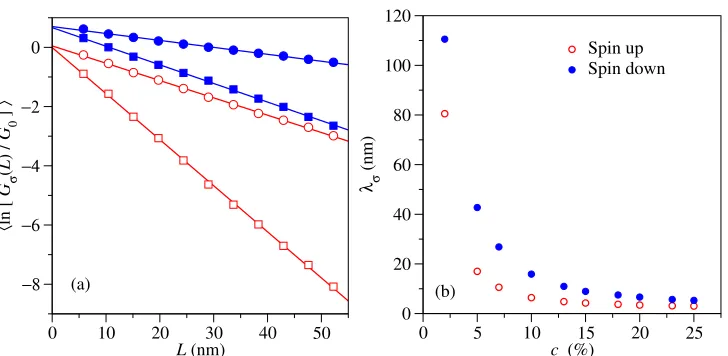
According to the one-parameter scaling theory of disordered systems introduced by Abrahams et al. [26], the conductance vanishes exponentially upon increasing the system length G(L) ∼ exp(−γL) with decay parameter γ. It turns out that G is log-normal distributed and for this reason we calculate hlogGσ(L)i ∼ −Lhγσi, where h· · ·i
stands for average over disorder realisations. This allows us to find a characteristic average localisation length λσ = 1/hγσi. The localisation length depends not only
on the spin direction but also on E, c and W. Figure 5(a) shows hlogGσ(L)i as a
function of the nanoribon lengthL. If we set the Fermi level of the system at the energy
0 10 20 30 40 50
L (nm)
−8 −6 −4 −2 0 〈 ln [ Gσ ( L ) / G0 ] 〉 (a)
0 5 10 15 20 25
c (%)
[image:10.612.117.481.84.262.2]0 20 40 60 80 100 120 λσ (nm) Spin up Spin down (b)
Figure 5. Average logarithm of the spin-dependent conductance as a function of (a) lengthL and (b) concentration c of a silicene nanoribbon of width W = 2.35 nm and M = 0.1 eV. The Fermi level is 0.95 eV and results were averaged over 1000 disorder realisations of samples. Error bars are smaller than symbol size. Vacancy concentrations are 0.05 (circles) and 0.10 (squares) in (a).
very different. To be specific, their values are λ↑ = 17 nm for spin-up electrons and
λ↓ = 43 nm for spin-down electrons when c = 0.05. Notice that λ↑ is smaller than system length L = 23.22 nm in figure 2 while λ↓ is much larger. This explains why only spin-down electrons can contribute to the electric current passing through the nanoribbon. Similarly, for a concentration of c= 0.10 (square), the localisation length is λ↑ = 6 nm and λ↓ = 16 nm. The localization lengths are therefore less than the chosen lengthL, but larger than the widthsW for each chosen concentration. Still, the random distribution of vacancies produce a strongly spin-dependent localisation effect on the electrons that eventually leads to a weighted polarisation close to that found in pristine nanoribbons. The dependence of the localisation length as a function of vacancy concentration is shown in figure 5(b). For lower values of concentration, the difference between localisation lengths is greater. This difference decreases as the concentration increases, as expected. High values of the polarisation are expected when the condition
λ↑(E)< L < λ↓(E) at the Fermi energy is met.
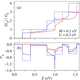
Finally, we briefly discuss the effects of a perpendicular electric field E on the performance of the spin-filter device. This amounts adding a term of the form
UP
iσζic
†
iσciσ to the Hamiltonian (1). Here ζi = +1 (ζi = −1) for sites in the A (B)
sublattice andU =eEdwithd= 0.03 nm. Electrics fields open a gap, being of the order of 2U in the case of strong fields (U λSO) [7]. Figure 6 shows the spin-dependent
electrons in the clean sample when the Fermi energy is in the range between 0.2 eV and 0.4 eV. This energy window is wide enough to be of practical interest in applications but polarisation is degraded to some extend in the presence of disorder since it reduces 50% when the concentration of vacancies is c = 0.01. This is in contrast to what we previously found in the energy range E = 0.85−0.95 eV, shown as a shaded area in figure 2, where polarisation is robust against disorded induced by vacancies.
0
1
2
3
4
〈
G
σ〉
/
G
00.0
0.5
1.0
1.5
E
(eV)
−1.6
−1.2
−0.8
−0.4
0.0
P
σ(a)
(b)
M
= 0.1 eV
[image:11.612.163.429.194.462.2]U
= 0.3 eV
Figure 6. (a) Spin-dependent conductanceGσ (σ=↑,↓) as a function of energy of a
silicene nanoribbon of widthW = 2.35 nm and lengthL= 23.22 nm whenM = 0.1 eV. Solid lines correspond to the average over 100 disorder realisations of samples with vacancy concentration c = 0.01 and dashed lines indicate the conductance of the clean sample. The electric potential due to a perpendicular electric field is 0.3 eV (b) Corresponding energy-dependent weighted polarization per spin.
4. Conclusions
proper selection of the system parameters (Fermi energy E, vacancy concentration c
and system length L) allows the nanoribbon to act as an efficient spin filter. We have also considered the effects of a perpendicular electrid field. At low energy the spin-down weighted polarisation in clean samples is high over a wide energy region but it rapidly degrades upon increasing the vacancy concentration. On the contrary, in the absence of electric field we have demonstrated that there exist certain energy windows where the polarisation of disordered samples are similar to the clean one. This happens when
λ↑(E) < L < λ↓(E) since only spin-down electrons can pass through the system and reach the drain contact. Therefore, we conclude the effect is robust against moderate disorder in some particular energy ranges and that the proposed device is a promising candidate for real-world applications in spintronics.
Acknowledgments
C. N. and F. D-A. thanks the Theoretical Physics Group of the University of Warwick for the warm hospitality. Work in Madrid was supported by MINECO (grant MAT2013-46308). L. R. and P. A. O. acknowledge support from FONDECYT (grants 1140388 and 1140571) and CONICYT (grant ACT 1204). R. A. R. is grateful to the EPSRC for financial support (EP/J003476/1). We acknowledge provision of computing resources through the MidPlus Regional HPC Centre (EP/K000128/1). All data are provided in full in the results section of this paper.
References
[1] A H Castro Neto, Guinea F, Peres N M R, Novoselov K S and Geim A K 2009 Review Modern Physics 81109
[2] Aufray B, Kara A, Vizzini S, Oughaddou H, Landri C, Ealet B and Le Lay G 2010Applied Physics Letters 96183102
[3] De Padova P, Quaresima C, Ottaviani C, Sheverdyaeva P M, Moras P, Carbone C, Topwal D, Olivieri B, Kara A, Oughaddou H, Aufray B and Le Lay G 2010 Applied Physics Letters 96
261905
[4] Lalmi B, Oughaddou H, Enriquez H, Kara A, Vizzini S, Ealet B and Aufray B 2010Applied Physics Letters 97223109
[5] Liu C C, Feng W and Yao Y 2011Physical Review Letters 107076802 [6] Kane C L and Mele E J 2005 Physical Review Letters 95226801 [7] Ezawa M 2012New Journal of Physics 14033003
[8] Calixto M and Romera E 2015EPL (Europhysics Letters)10940003 [9] Le Lay G 2015 Nature Nanotechnology 10202
[10] Tao L, Cinquanta E, Chiappe D, Grazianetti C, Fanciulli M, Dubey M, Molle A and Akinwande D 2015Nature Nanotechnology 10227
[11] Yamakage A, Ezawa M, Tanaka Y and Nagaosa N 2013Physical Review B 88085322
[12] Mun´arriz J, Dom´ınguez-Adame F, Orellana P A and Malyshev A V 2012 Nanotechnology 23
205202
[13] Saiz-Bret´ın M, Mun´arriz J, Malyshev A V and Dom´ınguez-Adame F 2015Physics Letters A379
[14] Mun´arriz J, Gaul C, Malyshev A V, Orellana P A, M¨uller C A and Dom´ınguez-Adame F 2013
Physical Review B 88155423
[15] D´ıaz E, Miralles K, Dom´ınguez-Adame F and Gaul C 2014Applied Physics Letters 105103109 [16] Haugen H, Huertas-Hernando D and Brataas A 2008Physical Review B 77 115406
[17] Swartz A G, Odenthal P M, Hao Y, Ruoff R S and Kawakami R K 2012ACS Nano 610063 [18] Lee Y L, Kim S, Park C, Ihm J and Son Y W 2010ACS Nano 41345
[19] Wang Sa-Ke, Tian Hong-Yu, Yang Yong-Hong and Wang Jun 2014Chinese Physics B 23017203 [20] Anderson P W 1958Physical Review 1091492
[21] Haldane F D M 1988Physical Review Letters 612015
[22] Lambert C J and Weaire D 1980physica status solidi (b) 101591 [23] Landauer R 1970Philosophical Magazine 21863
[24] Datta S 1995Electronic Transport in Mesoscopic Systems (Cambridge University Press) [25] Gao J, Zhang J, Liu H, Zhang Q and Zhao J 2013Nanoscale 59785