>XylogiCS)
Model 712
}User's
Manual
YOUR PARTNER FOR PERFORMANCE.
166-712-001
Revision A
September 22, 1986
. .;.
XYLOOlCS 712 Disk Controller User's Manual
RE.VISlOO
I
A (9/22/86) Al (12/1/86)712 RE.VISlQil LEVEL HISroRY
DESOUPl'lON
Ini tial release.
Added VME canp1iance number to Section 1.8. Technical addition to Section 4.2 (Controller Parameters lOPS): Byte OC now contains the 712 Release Level; bit 5 in Byte 08 is nCM Disable ACFAIL (~CF); added Section 4.2.5. Edited Sections 4.2.3 (ASR), 4.2.8, 4.2.9, 6.1.2.4 (Code 45), 8.4, and 8.4.1.
tOlE
Only the Table of Contents, Section 4, and pages 6, 54, 58, 80, 89, 91, and 112 are marked Rev. Al.
)xylogics)
Model 712
User's Manual
YOUR PARTNER FOR PERFORMANCE.
166-712-001
Revision A
XYLOOIQ) 712 Disk Controller User I s Manual
LIS'l' OF ~TIQqS ••••••••••••••••••••••••••••••••••••••••••••••• xi
SECrIOO 1: SPECIFICATIONS
1.0 ~ •••••••••••••••••••••••••••••••••••••••••••••••••••••••• 1
1.1 {5~ 'nIIS .MMtJAI, •••••••••••••••••••••••••••••••••••••••••••••• 1 1.1.1 Abbreviations •••••••••••••••••••••••••••••••••••••••••• 1
1.2 DESI~ .RE:[,IABn..I'l'!l ••••••••••••••••••••••••••••••••••••••••••••• 2
1.3 HlYSlCAI.. •••••••••••••••••••••••••••••••••••••••••• ~... 3
1.4 •••••••••••••••••••••••••••••••••••••••••••••••••• 3
1.5 E:r.EX:'m.ICAI.. •••••••••••••••••••••••••••.•••••••••••••••••••••••••• 3
1.6 SYS'.r9t RELA'J."EI) SPECIFICATIOOS •••••••••••••••••••••••••••••••••• 4
1.7 DISK DRIVE REI.A'lm SPECIFICATIOOS •••••••••••••••••••••••••••••• 5
1.8 VMEbus ~ SPECIFlCA~S •••••••••••••••••••••••••••••••••• 6
1.9 ~ REI.aAim SPECIFlCATIOOS •••••••••••••••••••••••••••••••• 7
1.9.1 SOftware Interface ••••••••••••••••••••••••••••••••••••• 7
1.10 ~ ~ •••••••••••••••••••••••••••••••••••••••••• 8
SECTIOO 2:
2.0
2.1
2.2
GENERAL •••••••••••••••••••••••••••••••••••••••••••••••••••••••• 9
UNPACKING AND INSPECTION •••••••••••••••••••••••••••••••••••••••
92.1.1 2.1.2 2.1.3 2.1.4
Inspect the Shipping carton •••••••••••••••••••••••••••• 9 Contents ••••••••••••••••••••••••••••••••••••••••••••••• 9
Handling Precautions ••••••••••••••••••••••••••••••••••• 9
Inspect the 712 •••••••••••••••••••••••••••••••••••••••• 9
CONFI~ THE 712 ••••••••••••••••••••••••••••••••••••••••••• 10
2.2.1 2.2.2 2.2.3
Base Address Selection •••••••••••••••••••••••••••••••• 11 Bus Request and Bus Grant Lines ••••••••••••••••••••••• 11 Parallel Arbitration •••••••••••••••••••••••••••••••••• 12
i
XXLUiIu) 1.1.:l U1SK u>nUO.1..1.er user' s 1'JallUa.L
2.3
2.4
2.5
2.6
2.7
2.8
2.9
2.10
2.11
PROMS AND PALS •••••••••••••••••••••••••••••••••••••••••• ~ ••••• 12
SELF TEST DISABLE ••••••••••••••••••••••••••••••••••••••••••••• 13
PROMS AND PALS •••••••••••••••••••••••••••••••••••••••••••••••• 13
LIGHT EMITTlNG DIODES ••••••••••••••••••••••••••••••••••••••••• 13
BOARD LABELS / REVISION CONTROL ••••••••••••••••••••••••••••••• 13
2.8.1 2.8.2 2.8.3
•••••••••••••••• 14
Ba~lane
Jumpers ••••••••••••••••••••••••••••••••••••• 14
card cage Slot •••••••••••••••••••••••••••••••••••••••• 14 Power Considerations •••••••••••••••••••••••••••••••••• 14
PREPAR]N; 'DIE DISK DRIVE FOR INSTALLATION ••••••••••••••••••••• 14
2.9.1 2.9.2 2.9.3
Drive Unit Select ••••••••••••••••••••••••••••••••••••• 15
NUmber
ofSectors Per Track •••••••••••••••••••••••••••
15Sector and Index PUlses ••••••••••••••••••••••••••••••• 16 INSTALL AND CABLE '!HE 712 ••••••••••••••••••••••••••••••••••••• 16
2.10.1
2.10.2 Insta:Ll
tlle 712 •••••••••••••••••••••••••••••••••••.•••• cable tlle Subsystem ••••••••••••••••••••••••••••••••••• 16 16
INITiAL ~ ••••••••••••••••••••••••••••••••••••••••••••••••• 17
2.11.1 2.11.2
Power-up and Self Test •••••••••••••••••••••••••••••••• 17
~ive
Reaqy •••••••••••••••••••••••••••••••••••••••••••
17
2.12 DIAGNOSTICS ••••••••••••••••••••••••••••••••••••••••••••••••••• 17
2.13
2.13.1 2.13.2 2.13.3 2.13.4
•••••••••••••••••••••••••••••••••••••••
Te~tor ••••••••••••••••••••••••••••••••••••••••••••
•••••••••••••••••••••••••••••••
(Daisy-chain)
(Radial) •••••••••••••••••••••••••••••••••••• Unit Select •••••••••••••••••••••••••••••••••••••••••••
17
18 18 18 18
SECl'IOO 3: '!HE 712 RmISTERS
3.0 GENERAL ••••••••••••••••••••••••••••••••••••••••••••••••••••••• 19
3.1 lOPS ~S RmISTERS •••••••••••••••••••••••••••••••••••••••• 19
ii
xn.cx;lCS 712 Disk Controller User I s Manual
Pl!GE
3.2 lOPS AI>I:mSS K>DIFIER / PRIORITY lOPS RIDISTER •••••••••••••••• 19
3.3 CONTROL AND ST~S REGISTER ••••••••••••••••••••••••••••••••••• 20
3.3.1 3.3.2
Control Register (Write) •••••••••••••••••••••••••••••• 20 Status Register (Read) •••••••••••••••••••••••••••••••• 22
3.4 FA~ ERROR RIDlSTER •••••••••••••••••••••••••••••••••••••••••• 24
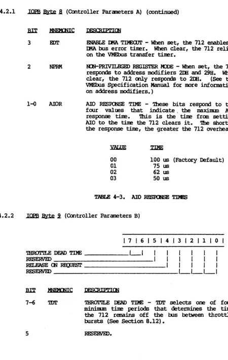
SECI'lON 4: lOPS D&SClUPl'ION
4.0 ~ •••.••••..•••.. .••.•••..•.••.••...••.•••.•••••••••••••• 25
4.1 STANDARD lOPS ••••••••••••••••••••••••••••••••••••••••••••••••• 25
4.1.1 4.1.2 4.1.3 4.1.4 4.1.5 4.1.6 4.1.7 4.1.8 4.1.9 4.1.10 4.1.11 4.1.12 4.1.13 4.1.14 4.1.15 4.1.16 4.1.17 4.1.18 4.1.19
lOPS B¥te 0 (Command) ••••••••••••••••••••••••••••••••• 26 lOPS B¥te 1 (status Byte 1) ••••••••••••••••••••••••••• 26 lOPS B¥te 2 (status Byte 2) ••••••••••••••••••••••••••• 27 lOPS B¥te 3 (status Byte 3) ••••••••••••••••••••••••••• 27 lOPS B¥te 4 (Subfunction) ••••••••••••••••••••••••••••• 27
lOPS
B¥te
5 (Unit) •••••••••••••••••••••••••••••••••••• 29lOPS B¥te 6 (Interrupt Level) ••••••••••••••••••••••••• 30 lOPS B¥te 7 (Interrupt Vector) •••••••••••••••••••••••• 31 lOPS Bytes 8 and 9 (Count) •••••••••••••••••••••••••••• 31 lOPS B¥tes A and B (GY1inder) ••••••••••••••••••••••••• 31 lOPS B¥te C (Head) •••••••••••••••••••••••••••••••••••• 31 lOPS B¥te D (Sector) •••••••••••••••••••••••••••••••••• 31 lOPS B¥te E (Data or Link Address Modifier) ••••••••••• 31 lOPS Byte F (Next lOPS Address Modifier) •••••••••••••• 32 lOPS B¥tes 10 'lbrough 13 (GtA Data Address) ••••••••••• 32 lOPS B¥tes 14 'lhrough 17 (Next lOPS Address) •••••••••• 32 lOPS Bytes 18 and 19 (lOPS Checksum) •••••••••••••••••• 32 lOPS
B¥tes
1A and 1B (ECC Pattem Word) ••••••••••••••• 32 lOPS Bytes 1C and 10 (ECC Offset Word) • • • • • • • • • • • • • • •• 334.2 CONTROLLER PARAMETERS lOPS •••••••••••••••••••••••••••••••••••• 33
4.2.1 4.2.2 4.2.3 4.2.4 4.2.5 4.2.6 4.2.7 4.2.8 4.2.9
lOPS B¥te 8 (Controller Parameters A) ••••••••••••••••• 34 lOPS B¥te 9 (Controller Parameters B) ••••••••••••••••• 35 lOPS B¥te A (Controller Parameters C) ••••••••••••••••• 36 lOPS B¥te B (Controller Parameters D) ••••••••••••••••• 37 lOPS B¥te C (Release Level) ••••••••••••••••••••••••••• 38 lOPS B¥te E (Controller
TYPe) •••••••••••••••••••••••••
38 lOPSB¥tes
10 and II (EPRCM Part Number) •••••••••••••• 38 lOPS B¥te 12 (Revision) ••••••••••••••••••••••••••••••• 38 lOPS B¥te 13 (Subrevision) •••••••••••••••••••••••••••• 38iii
XYUX;IQ) 712 Disk Controller User I s Manual
4.3 DRIVE p~ DOPS ••••••••••••••••••••••••••••••••••••••••• 39
4.3.1 4.3.2 4.3.3 4.3.4 4.3.5 4.3.6 4.3.7
lOPS ~ 6 (Drive Parameters) •••••••••••••••••••••••• lOPS Byte 8 (Max Sector/Last Head) •••••••••••••••••••• DOPS Byte 9 (Head Offset) •••••••••••••••••••••••••••••
lOPS Bytes A and B (Max C¥linder) •••••••••••••••••••••
••••••••••••••••••••••••••••••••
lOPS ~ C (Max Head)
lOPS Byte D (Max Sector) ••••••••••••••••••••••••••••••
lOPS ~ E (Sectors Per Track) •••••••••••••••••••••••
39 40 41 41 41 41 41
4.4 FORMAT PARAMETERS lOPS •••••••••••••••••••••••••••••••••••••••• 42
4.4.1 4.4.2 4.4.3 4.4.4 4.4.5 4.4.6 4.4.7 4.4.8 4.4.9 4.4.10 •••••••••••••••••••••••••••••• (Interleave) (Field 1) lOPS Byte 9 (Field 2) lOPS Byte A (Field 3) lOPS Byte B (Field 4) lOPS Byte 6
lOPS Byte 8 •••••••••••••••••••••••••••••••••
•••••••••••••••••••••••••••••••••
••••••••••••••••••••••••••••••••• •••••••••••••••••••••••••••••••••
lOPS Bytes C and D (Field 5 High/Low) ••••••••••••••••• lOPS Byte E (Field 12)
lOPS Byte 10 (Field 6) lOPS Byte 11 (Field 7)
•••••••••••••••••••••••••••••••• •••••••••••••••••••••••••••••••• ••••••••••••••••••••••••••••••••
lOPS Bytes 12 and 13 (Al ternate Field 5 High/Low) •••••
SEcrION 5: ~
5.0 5.1 5.2 5.0.1 5.0.2 •••••••••••••••••••••••••••••••••••••••••••••••••••••••
Setting Up The Canmmd canpleting The Canmmd
••••••••••••••••••••••••••••••••
••••••••••••••••••••••••••••••••
••••••••••••••••••••••••••••••••••••••••••••••••••
WRITE DATA ••••••••••••••••••••••••••••••••••••••••••••••••••••
42 43 43 43 44 44 44 44 44 44 45 45 45 46 47
5.3 READ ~ ••••••••••••••••••••••••••••• ~ ••••••••••••••••••••••• 48
5.4 REPORT CURRENT ADCRESS •••••••••••••••••••••••••••••••••••••••• 49
5.5 SEEJC AND REroRT 0JRRmr ADIJU::SS ••••••••••••••••••••••••••••••• 50 5.6 STAR!' SEEK AND REFORT <DtPLETION IMMEDIATELY •••••••••••••••••• 51
5.7 DRIVE RESETWI1H ~ TO ZERO ••••••••••••••••••••••••••••••• 52
5.8 FAULT CLEAR ••••••••••••••••••••••••••••••••••••••••••••••••••• 53
5.9 WRITE a:Nl'RCLLER PARAMETERS ••••••••••••••••••••••••••••••••••• 54
5.10 ~TE DRIVE PARAMETERS •••••••••••••••••••••••••••••••••••••••• 55
iv
xnroIa; 712
Disk Controller User's
ManualPAGE
5.11 WRITE FORMAT PARAMETERS •••••••••••••••••••••••••••••••••• ~ ••• 56
5.12 STORE FORMAT CONFIGURATION •••••••••••••••••••••••••••••••••••• 57
5.13 READ OONTROLLER PARAMETERS •••••••••••••••••••••••••••••••••••• 58
5.14 READ DRIVE PARAMETERS ••••••••••••••••••••••••••••••••••••••••• 59
5.15 READ ~RMAT PARAMETERS •••••••••••••••••••••••••••••••••••••••• 60
5.16 READ DRIVE STAmS EXTENDED •••••••••••••••••••••••••••••••••••• 61
5.17 SHOW DRIVE CONFIGURATION •••••••••••••••••••••••••••••••••••••• 62
5.18 ••••••••••••••••••••••••••••••••••••••••••• 63
5.19 WRITE 'mA.CX FORMAT •••••••••••••••••••••••••••••••••••••••••••• 64
5.20 WRITE HEADER, HEADER VERIFY, MTA, AND MTA ECC
...
655.21 WRITE DEE'ECl' MAP' •••••••••••••••••••••••••••••••••••••••••••••• 66
5.22 READ 'mA.CX. HEADERS •••••••••••••••••••••••••••••••••••••••••••• 67
5.23 VERIFY MTA ••••••••••••••••••••••••••••••••••••••••••••••••••• 68
5.24 READ HEADER, HEADER VERIFY, MTA, AND MTA ECC •••••••••••••••• 69 5.25 READ DEFECl' MAP' ••••••••••••••••••••••••••••••••••••••••••••••• 70
5.26 ••••••••••••••••••••••••••••••••••••••••••••••••••• 71
5.27 ESDI COMMAND WITBOOT ~ ••••••••••••••••••••••••••••••••••• 72
5.28 ESDI COMMAND WITH ~s
••••••••••••••••••••••••••••••••••••••
73SECl'IOO 6: ERROR P.R<XESSlm
6.0
6.1
••••••••••••••••••••••••••••••••••••••••••••••••••••••• 75
'mE <Dtl?J:..E'l1IOO' (XJ)E ••••••••••••••••••••••••••••••••••••••••••• 75
6.1.1 6.1.2
Oompletion
CodeConvention ••••••••••••••••••••••••••••
75Completion
CodeDescriptions ••••••••••••••••••••••••••
77-v-_ -v-_ -v-_ - 1 - _ _ ,
XYL<xnQ; 712 Disk Controller User I s Manual 6.2 6.3 6.4 6.5 6.6 PN3E
••••••••••••••••••••••••••••••••• 83
••••••••••••••••••••••••••••••••••• 83
ERROR CORRECTION COCE ••••••••••••••••••••••••••••••••••••••••• 84
6.4.1 6.4.2 6.4.3
Error Correction COde Error Correction COde Error Correction COde
FATAL ERROR CODE DESCRIPl'lONS
Mode 0
Mode 1
Mode 2
•••••••••••••••••••••••• •••••••••••••••••••••••• •••••••••••••••••••••••• ••••••••••••••••••••••••••••••••• 84 84 84 85
IRl\M CliE<XS(JM ••••••••••••••••••••••••••••••••••••••••••••••••• 86
SEcrlON 7: A 'lUTORIAL IN PROORAMM:lN; '!HE 712
7.0 7.1 7.2 7.3 7.4 7.5
~ ••••••••••••••••••••••••••••••••••••••••••••••••••••••• 87
00 OPERA.TIOO •••••••••••••••••••••••••••••••••••••••••••••••••• 87
7.1.1 7.1.2 7.1.3 7.1.4 7.1.5 7.1.6
Allocating Memory For An lO:PS ••••••••••••••••••••••••• 88 Point the 712 to the lOPS ••••••••••••••••••••••••••••• 88 Starting the Operation •••••••••••••••••••••••••••••••• 88
712 Operation ••••••••••••••••••••••••••••••••••••••••• 88
Command ~letion •••••••••••••••••••••••••••••••••••• 88
Returned Values ••••••••••••••••••••••••••••••••••••••• 89
READ <XNrRCLLER PARAMETERS •••••••••••••••••••••••••••••••••••• 89
7.2.1 7.2.2 7.2.3
Execute the lOPS •••••••••••••••••••••••••••••••••••••• 90
712 Operation ••••••••••••••••••••••••••••••••••••••••• 90
The Returned lOPS ••••••••••••••••••••••••••••••••••••• 90
WRITE CXNrRa.J..ER PARAMETERS ••••••••••••••••••••••••••••••••••• 90 7.3.1 712 Operation ••••••••••••••••••••••••••••••••••••••••• 91
READ/WRITE DRIVE PARAMETERS ••••••••••••••••••••••••••••••••••• 92 7.4.1 712 Operation ••••••••••••••••••••••••••••••••••••••••• 92
READ/WRITE FORMAT PARAMETERS •••••••••••••••••••••••••••••••••• 93
7.5.1 7.5.2 7.5.3 7.5.4
Execute the lOPS with Interrupts •••••••••••••••••••••• 94 712 Operation ••••••••••••••••••••••••••••••••••••••••• 94 COmmand ~letion •••••••••••••••••••••••••••••••••••• 94
Returned Values ••••••••••••••••••••••••••••••••••••••• 94
vi
m..cx;ICS 712 Disk Controller User' s Manual 7.6 7.7 7.8 7.9 7.10 7.11 PAGE
FORMAT A TRACK •••••••••••••••••••••••••••••••••••••••••••••••• 94
7.6.1 712 q,eration ••••••••••••••••••••••••••••••••••••••••• 95
RF.AD 'mA.Cl< HEADERS •••••••••••••••••••••••••••••••••••••••••••• 96
7.7.1 7.7.2
712 q,eration ••••••••••••••••••••••••••••••••••••••••• 97
Veri~ing the Data •••••••••••••••••••••••••••••••••••• 98
WRITE DATA •••••••••••••••••••••••••••••••••••••••••••••••••••• 99
7.8.1 7.8.2
712 q,eration •••••••••••••••••••••••••••••••••••••••• 100 Command Completion ••••••••••••••••••••••••••••••••••• 100
RE.AD DATA •••••••••••••••••••••••••••••••••••••••••••••••••••• 100 7.9.1
7.9.2 7.9.3
712 q,eration •••••••••••••••••••••••••••••••••••••••• Command Completion ••••••••••••••••••••••••••••••••••• Veri~ Data ••••••••••••••••••••••••••••••••••••••••••
100 100 101
MULTiPLE SECTOR TRANSFERS •••••••••••••••••••••••••••••••••••• 102
~y •••••••••••••••••••••••••••••••••••••••••••••••••••••• 102
SECrION 8: 712 SPECIAL EUNCl'IONS
8.0
8.1
8.2
8.3
•••••••••••••••••••••••••••••••••••••••••••••••••••••• 103
MEDIA DEFECl' HANDLJR; •••••••••••••••••••••••••••••••••••••••• 103 8.1.1
8.1.2 8.1.3 8.1.4
Slipping a Sector •••••••••••••••••••••••••••••••••••• 103 Qylinder Sparing ••••••••••••••••••••••••••••••••••••• 105
~ack Remapping •••••••••••••••••••••••••••••••••••••• 106
Recamnended Remapping Procedure •••••••••••••••••••••• 106
CllAlNJR; AND MJLTIPLE
I/o
RFlJUF,SlS ••••••••••••••••••••••••••• 106 8.2.1 8.2.2 8.2.3 8.3.1 8.3.2 8.3.3 8.3.4Olaining ••••••••••••••••••••••••••••••••••••••••••••• 1 C17 Multiple I/O Requests •••••••••••••••••••••••••••••••• 107 712 Operation •••••••••••••••••••••••••••••••••••••••• 107
...
107 Allocating Spare Sectors ••••••••••••••••••••••••••••• 107Speci~ Sector Data Size ••••••••••••••••••••••••••••• 108
Speci~ Sector Gap Size •••••••••••••••••••••••••••••• lOS
Format Interleave •••••••••••••••••••••••••••••••••••• III
vii
TABLE OF <Xl'lI'.I!NlS
PAGE
8.4 ERROR REOOYERY ••••••••••••••••••••••••••••••••••••••••••••••• 112
8.4.1 8.4.2 8.4.3
Automatic Operation Ret~ •••••••••••••••••••••••••••• 112 ECCError Recove~ ••••••••••••••••••••••••••••••••••• 112 Using the Error Recove~ Options ••••••••••••••••••••• 113
8.5 READ DEFECT MAP •••••••••••••••••••••••••••••••••••••••••••••• 113
8.6
8.5.1 8.5.2
Manufacturer's Defect Map •••••••••••••••••••••••••••• 113 Read the Defect Map •••••••••••••••••••••••••••••••••• 113
MA:IN'I'ENANCE K>DE ••••••••••••••••••••••••••••••••••••••••••••• 113
8.6.1 8.6.2
Register Use in Maintenance Mode ••••••••••••••••••••• 113 Maintenance Mode Protocol •••••••••••••••••••••••••••• 114
8.7 ZERO ~CY ~ ••••••••••••••••••••••••••••••••••••••••••• 116
8.8
8.9
KJLTIPROCESSOR SUPR)Rl' ••••••••••••••••••••••••••••••••••••••• 116 8.8.1
8.8.2 8.8.3
Interrupts ••••••••••••••••••••••••••••••••••••••••••• 116 Register Busy Semaphore •••••••••••••••••••••••••••••• 116 Address Modifiers •••••••••••••••••••••••••••••••••••• 117
<DMMAND OPrIMlZATION ••••••••••••••••••••••••••••••••••••••••• 117 8.10 SOFTWARE OONT.ROL ••••••••••••••••••••••••••••••••••••••••••••• 117
8.10.1 8.10.2 8.10.3 8.10.4 8.10.5
Modi~ing a Single Parameter ••••••••••••••••••••••••• 117
Modi~ing a Group of Parameters •••••••••••••••••••••• 118
Parameter Reference Point •••••••••••••••••••••••••••• 118 Setting Parameters at Boot Time •••••••••••••••••••••• 118 Validate CUrrent Parameters •••••••••••••••••••••••••• 118
8.11 SCA~GATHER ••••••••••••••••••••••••••••••••••••••••••••••• 118
8.12
8.11.1 8.11.2 8.11.3 8.11.4
scatter/Gather Link List ••••••••••••••••••••••••••••• 118 setting Up a Scatter/Gather Transfer ••••••••••••••••• 119 712 Operation •••••••••••••••••••••••••••••••••••••••• 121 Zero Latency Reads and Scatter/Gather •••••••••••••••• 121
Dm '1BROI'.ILE / 'llmorJLE DEAD TIME •••••••••••••••••••••••••••• 121 8.13 BLACK HOLE TRANSFERS ••••••••••••••••••••••••••••••••••••••••• 121
viii
[image:14.615.54.520.52.695.2]XYJ.roIQ) 712 Disk Controller User I s Manual
PAGE
8.14 PRIOBXTY IOPBs ••••••••••••••••••••••••••••••••••••••••••••••• 122
8.14.1 8.14.2 8.14.3
Executing a Priority lOPS •••••••••••••••••••••••••••• 122 Executing a Priority Chain ••••••••••••••••••••••••••• 122
712 Response to a Priority lOPS (Chain) •••••••••••••• 122
8.15 ·DOPS CHECKSOM •••••••••••••••••••••••••••••••••••••••••••••••• 123
8.16 FIXED/REXNABLE MEDIA •••••••••••••••••••••••••••••••••••••••• 123
8.16.1 Bead Offset •••••••••••••••••••••••••••••••••••••••••• 123
8.17 EMBEDDED S~ DRIVES •••••••••••••••••••••••••••••••••••••••• 123
8.18
8.19
8.20
SUPIORl'lm FOOR DRIVES WI'lH DIFFERENT SECl'OR SIZES ••••••••••• 123
8.18.1 8.18.2 8.18.3
8.19.1
Setting the 712 Format Parameters •••••••••••••••••••• 123 Setting the 712 Drive Parameters ••••••••••••••••••••• 124 Accessing Drives With Alternate Fields ••••••••••••••• 124
••••••••• 124
Sbnulating an ECC Error •••••••••••••••••••••••••••••• 125 •••••••••••••••••••••••••••••••••••• 126
8.21 ~E ON R!CUEST ••••••••••••••••••••••••••••••••••••••••••• 126
SECrION 9: 712 'JBE()RY OF OPERATICfi
9.0 GENERAL •••••••••••••••••••••••••••••••••••••••••••••••••••••• 127
9.1 ~ Hardware ••••••••••••••••••••••••••••••••••••••••••••••••• 127
9.1.1 9.1.2 9.1.3 9.1.4 9.1.5
9.i.6
9.1.7 9.1.8 9.1.9 9.1.10
VMEbus Interface ••••••••••••••••••••••••••••••••••••• 127 Register Rea~rite and Interrupt •••••••••••••••••••• 128
The Microoontro11er •••••••••••••••••••••••••••••••••• 128 Direct Memory Access Controller •••••••••••••••••••••• 129 Disk Data Buffer ••••••••••••••••••••••••••••••••••••• 130 Disk Front End ••••••••••••••••••••••••••••••••••••••• 130 Enhanced Small Device Interface •••••••••••••••••••••• 130 PoWer-up ••••••••••••••••••••••••••••••••••••••••••••• 131
PoWe~ ••••••••••••••••••••••••••••••••••••••••••• 131
~stem Reset ••••••••••••••••••••••••••••••••••••••••• 131
-
9.2
9.3
9.4
PAGE
THE MICROCODE •••••••••••••••••••••••••••••••••••••••••••••••• 131
9.2.1 9.2.2 9.2.3 9.2.4 9.2.5
'!he Kernel ••••••••••••••••••••••••••••••••••••••••••• Is AIO Set? •••••••••••••••••••••••••••••••••••••••••• Is start Queue Empty? •••• ~ •••••••••••••••••••••••••••
Is Any IOPB
Reaqy
for Completion? •••••••••••••••••••• Queuing IOPBs for Execution ••••••••••••••••••••••••••131 131
1~2
133 133
PERFORMOO A FUNCrION •••••••••••••••••••••••••••••••••••••••• 133
9.3.1 9.3.2 9.3.3 9.3.4 9.3.5 9.3.6 9.3.7
NDP •••••••••••••••••••••••••••••••••••••••••••••••••• 133 Normal Reads and Writes •••••••••••••••••••••••••••••• 133 Seeks •••••••••••••••••••••••••••••••••••••••••••••••• 134 Drive Reset •••••••••••••••••••••••••••••••••••••••••• 134 Write and Read Parameters •••••••••••••••••••••••••••• 134 Extended Read and Write Commands ••••••••••••••••••••• 135 Diagnostics •••••••••••••••••••••••••••••••••••••••••• 135
COMP.LETOO A FUNCTION •••••••••••••••••••••••••••••••••••••••• 136
SECl'ION 10: MAINTENANCE AIDES
10.0 ~ •••••••••••••••••••••••••••••••••••••••••••••••••••••• 137
10.1 VMEbus INTERFACE SIGNALS ••••••••••••••••••••••••••••••••••••• 137
10.2 ENHANCED SMALL DEVICE INTERFACE •••••••••••••••••••••••••••••• 140
nIDEX •••••••••••••••••••••••••••••••••••••••••••••••• ~ • • • • • • • • • • • •• 143
XYLCX;lCS 712 Disk Controller User's Manual FlGJRm 2-1. 2-2. 2-3. 2-4. 2-5. 7-I. 7-2. 7-3. 7-4. 7-5. 7-6. 7-7. 7-8. 7-9. 7-10. 8-I. 8-2. 8-3. 8-4. 8-5. 8-6. 8-7. 9-1. 2-1. 2-2. 3-I. 3-2. 4-1. 4-2. 4-3. 4-4. 4-5. 4-6. 5-1. 5-2. 6-1. 6-2. 8-1. 8-2. 8-3. 8-4. 8-5. 8-6.
712 - Component Location ••••••••••••••••••••••• 10
Base Address Jumper Block •••••••••••••••••••••• 11 Jump:!ring Bus Request and Bus Grant Levels ••••• 12
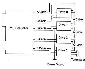
~le Part Number ••••••••••••••••••••••••••••• 13 cabling Multiple Drives •••••••••••••••••••••••• 18
~le NOP lOPS •••••••••••••••••••••••••••••••• 87 Sample Read Controller Parameters lOPS ••••••••• 89
~le Write Controller Parameters lOPS •••••••• 91
~le Write Drive Parameters lOPS ••••••••••••• 92
~le Read Format Parameters lOPS ••••••••••••• 93
~le Write Track Format lOPB ••••••••••••••••• 95 Sample Read Track Headers lOPB ••••••••••••••••• 97 Sample Sector Headers •••••••••••••••••••••••••• 98 Sample Write Data lOPB ••••••••••••••••••••••••• 99 Sample Read Data lOPB ••••••••••••••••••••••••• 101 Sector Slip ••••••••••••••••••••••••••••••••••• 103 NOr,ma} 712 Header ••••••••••••••••••••••••••••• 104 712 Header ~~ked Bad ••••••••••••••••••••••••• 104 712 Header Marked Spare ••••••••••••••••••••••• 104 712 Track Remap Header •••••••••••••••••••••••• 104 Sector Gap Sizes •••••••••••••••••••••••••••••• 109 Scatter/Gather Transfers •••••••••••••••••••••• 120 The 11icrooode Kernel •••••••••••••••••••••••••• 132
Base Address Selection ••••••••••••••••••••••••• 11 PROVPAL Part Number and Location •••••••••••••• 13 Reg'ister Offsets ••••••••••••••••••••••••••••••• 19 Fatal Error Codes •••••••••••••••••••••••••••••• 24 SUbfunction Code Classes ••••••••••••••••••••••• 28 712 camand/Subfunction Codes •••••••••••••••••• 28 AID Response Times ••••••••••••••••••••••••••••• 35 Throttle Values •••••••••••••••••••••••••••••••• 37 Controller Type Codes •••••••••••••••••••••••••• 38 712 Interleave Factors ••••••••••••••••••••••••• 43 712 Oammand Completion ••••••••••••••••••••••••• 45 Extended Drive Status •••••••••••••••••••••••••• 61
Recove~ Codes ••••••••••••••••••••••••••••••••• 75
SUmmary of Canpletion Codes •••••••••••••••• < • • • • 76
Reg'ister Use in Maintenance Mode •••••••••••••• 114 Scatter/Gather Link List •••••••••••••••••••••• 119 Link List Field Values •••••••••••••••••••••••• 119 Throttle Dead Time Values ••••••••••••••••••••• 121 EC32 VB. Returned Data •••••••••••••••••••••••• 124
SUnulated 2-bit Error Crossing Byte Boundaries 125
xi
XYLOGICS 712 Disk Controller User's Manual
~CB 1: SPECIFlCATICNS
1.0 GENERAL
'!be Xylogics Model 712 Disk Controller accamoodates up to four ESDI interface disk drives to
VMEbusl
systems.1.1 USJR;
mrs
MANUAL1.1.1
'lhis manual provides two Software Reference Cards for fast reference of the lOPB structure and codes (See insert). Section 2 describes how to install and test the 712; Section 3 describes the
712 registers; Section 4 describes the IOPSs; and Section 5
describes the 712 oammands. Section 6 describes error processing; Section 7 is a programming tutorial; Section 8 explains the 7l2's special functions; Section 9 describes the 712 theory of operation; and Section 10 includes maintenance aides.
Abbreyiations
'lhis manual uses the following mnemonics:
AFE
AIO AIOP AIOR »1 ASR ADD
BHT
<lIm OU'L
QUO
(l)p
oms
CrYP IFLT IIt1A
DRDY
OOKCEL OC32
Alternate Field Enable Idl New lOPB
AIO Pending
AIO Response Time Idlress Modifier Autaratic Seek Retry Auto-update
Black Hole Transfer Chain Enable
CQmnand carplete Clear Remove IOPB cannand Optimization Clear Register Busy Controller Type Drive Fault
Direct Memory Access Drive Ready
Disk Front End Chip 32-Bit ECC
1. VMEbus is a trademark of the Vf.!Ebus International Trade Association.
1.1.1 Abbreviations (continued) ECC ECQtt Em' ERRS ESD FERR FIFO H ICS
IEe
lOPS MBS RetA MM NPRM (}JS PNUM PRIO PSEL RBC RBS ROOCEL RIO RMM R)R SGM SKER TOr 'lHRO ~ VMEIJ1A WRP.r ZLRError Correction
Code
Error Cor rection Mode
Enable J:It1A Timeout Error Sunmaty
Embedded
Servo DriveFatal Error
First IQ/First OUt Disk Data Buffer
Notation For Numerical Values Expressed in Hexadecimal lOPS Ol.ecksum
Interrupt At End Of Olain Irput/Output Parameter Block
Megabytes Per
Secom
Maintenance Mode Active Maintenance Mode
Nal-privileged Register Mode
CNerlap seek Enable Pran Number
Priority lOPS Priority Select
Retry Before Cor rection Register Busy Semaphore
Register Read/Write and Interrupt Renove lOPS
Register Maintenance Mode Release On Request
Scatter/Gather Mode
Seek Error
'lbrottle Dead T.ime 'lbrottle
Transfer Mode
Direct Memory Access Controller QUp Write-protect
zero Latency Reads
1.2 DESIGN RELIABILITY
Xy10gics inplements the follOltling features to minimize the likelihood of product failure:
o Design for worst case voltage and temperature.
o Extensive evaluation testing.
o Low parts count through extensive use of custan ISI. o Buffer parity for continuous error checking.
x:n,cx;ICS 712 Disk Controller User I s Manual
1.2 DESIGN RELIABILITY (continued)
o LcM-stress design on all canponents.
o All canponents burned-in.
o One card; resides in backplane or expansion chassis.
o Ccntroller is power-cycled under thermal stress during test.
1.3 PHYSICAL
PACKAGIro board.
'!be 712 completely resides on one printed circuit DIMENSIOOS - '!be 712 is a 2 by 2 Eurocard standard; it measures 9.2-inches high by 6.3-inches deep (233.35 nm by 160 nm). 1be 712 is identical in form-factor to the standard VME (cilal high-dual wide) printed circuit board.
SHIPPm:; WEIGHT - 3 p>unds (1.4 kg).
FRCNI' PANEL - Xylogics offers the 712 wi th an optional front panel.
aNNECl'ORS - '!be ESDI connectors are on the edge of the board facing out; they protrude through the optional front panel. '!be
optional straight conrectors do not protrude the front panel.
1.4 ~
'lbe 712 envirormental requirements are 0 - 550 C, with a maximum relative humidity of 90% (without condensation). Air flow across the board must maintain a maxi.num temperature differential of 70 C
to prevent hot sp>ts.
1.5 ELECrRICAL
lOiER - 'lbe 712 uses 4.1 anperes at +5 volts DC (VDC).
rnLERAN<E - Voltage must be within plus or minus five percent (4.75 to 5.25).
GRClJN[)m:; - - Ccmoon earth ground must be established between the disk drives and the CPU chasSis, backplane, and expansion cabinets.
XYLUi~u) I J.~ D.lSK u:>nuoJ.J.er user' s tvJaIlUaI.
1.6 SYS'I'EN RELATID SPECIFlCATIOOS
DATA BUFFEROO - '!he 712 has a FIFO buffer that is 8k-bytes long and incorporates parity error detection. Data can be put into one end of the FIFO and simultaneously removed at the other end; there are no delays associated with filling and emptying the buffer.
KJLTIPLE IOPBs Cfi A Snl2LE RENCLtJ1'ION - '!be 712 can execute multiple IOPBs on a single revolution. For example, i f four ]oPBs for four sectors on the same head and cylinder are chained, the 712 can transfer the sectors into the buffer on a single revolution, and transfer each one out to the correct memory location.
PRIORITY IOPBs - '!he 712 executes priority IOPBs over all IOPBs in its cannand cache, except for the one in process.
roRMAT -
'!he 712 Format canmand formats a specified number of tracks. Use the Read/Write Headers camnands to incorporate custan interleaving schemes. Standard interleaving is 1:1; 2:1 to 15:1 interleaving is software programmable.MEDIA DEFECl'S - 'nle 712 has several nethods for remapping bad blocks. One nethod leaves spare sectors on each track that can be slipped with Read/Write Track Headers comn:ands. An alternate nethod has the spare sectors on the last part of the maximum track. '1he 712 also remaps entire tracks. '1bis lessens the total number of spare sectors required with minimal affect on 712 performance.
READ DEFECr MAP FEA'lURE - '1he 712 can read the manufacturer IS
defect information directly from the disk.
srA'lUS
LEns - '1he 712 implements two statusLEDs. Ll (BSY)indicates the controller is active; L2 (ERR) indicates the on-board diagnostics did not complete successfully, or a fatal error occurred.
SCA'rlER/GA'mER - '!be 712 supports Scatter/Gather on Read and Write oomnands. '!he controller can gather data from various memory locations and transfer it to the buffer for use in a Write command; it can scatter the data out fran the disk drive to the appropriate memory locations with a Read command. To execute a scatter/gather, software issues a normal Read or Write canmand along with a IJ.lA list that contains a memory address and the number of words to transfer to/fran that location. ']he smallest granularity of
scatter/gather is a l6-bit word.
XY.LOGICS 712 Disk Controller Userls Manual
1.6 SYS'.mo1 R.ELA'l'm SPECIFICATIONS (cxmtinued)
ERRm ~ION AND OORREX!rION - '!be 712 suptX>rts a 48-bit data EXX:; it cptionally suptX>rts a 32-bit data ECC. Software oontrols autanatic detection and oorrection.
']he 32-bit ECC detects an error OOrst up to 22-bits long, and corrects an error burst up to ll-bits long.
'!be 48-bit ECC detects an error burst up to 28-bits long, and corrects error bursts up to l4-bits long, assuring data integrity.
IMH.IED SEEX CAPABn.ITY - Data transfer instructions oontain an inplied seek. Data transfers cross sector, head, and cylinder boundaries as required (spiral read/write).
OJERI..AP SEEKS - '!be 712 supports overlap seeks. When overlap seeks are enabled, the 712 may have both drives simultaneously seeking to the appropriate cylinders.
ELE.VATOR SEEKS - When elevator seeks are enabled, the 712 reorders
cxmnands in ascending and then descending cylinder order to get the
best throughput fran the disk subsystem.
ZERO LATENCY READS - When the head arrives over the cylinder, the 712 reads the first sectors it finds that are included in the lOPS; it transfers the data to its own buffer and then out to the correct nenory location. ']he oontro11er finishes the track transfer when
the initial sectors arrive under the head.
BI.N:l{ HOLE 'mANSFERS - ']he 712 may transfer all the lEA data into the same bus address without incrementing the address at each lEA. SOF'lWARE SOPPORl' - Sanple software driver supplied for use in UNIX2 (5.0) based systems (source included).
1.7 DISK DRIVE RFLA'l'ID SPECIFICATIONS
mYSlCAL DRIVE INTERFACE - '1be 712 suworts the ESDI interface. INl'ERFACE DA.TA RATE AND S'1'ANDARD INrEK..EAVE FACTOR - '1be 712 supports a maxiDIlIn disk data rate of 1.2 Megabytes Per
Seoom
(MBS). '1be 712 suptX>rts this data rate at a 1:1 interleave factor. EJmEDDED SERVO DRIV&S - ']he 712 suWOrts embedded servo drives.
~ OF DISK DRIVES - '1be 712 suWOrts up to four ESDI disk drives.
DISK SECroR FORMAT - '1be 712 sector format includes a header field separated fran a data field by a splice area.
2. UNIX is a trademark of M&T.
1.7 DISK DRIVE RELATED SPECIFlCATIOOS (continued)
DISK SECrOR FORMAT - '!be 712 sector format includes a header field separated fran a data field by a splice area.
HEADER FORMAT - Header contains sector, head, cylinder address, and header
ate
or redundent header depending on i f your using. 48 or 32 bit ECC.
CABLIm - '!be 712 uses standard 20- and 34-pin flat ribbon cables.
'!be ma.xirmlm length of each cable is 3 neters (9.8 feet). 1.8 VMEbus RELATED SPECIFlCATIOOS
VME CXlrU?LIANCE NUMBER - IEEE P1014/Dl.0.
'lRANSFER foDDE - Direct Memory Access (IJ.1A).
II4A 'lHROl"lt.E aNmCL - Each tine the 712 becares bus master, it executes J:It1A transfers to or fran the buffer up to the max throttle limit or the number of bytes/spaces available in the buffer.
J:It1A DATA'mANSFER RATE - '!be 712 transfers data at a rate of up to 10 MBS; this rate requires Longword mode transfers and systan memory that responds within 200 nanoseconds.
J:It1A DEAD TIME - '!be 712 supports a programmable throttle dead tine between throttle bursts. '!his prevents the 712 fran taking over the bus and allows tine for other J:It1A devices to access the bus.
DATA 'lRANSFER LIMIT - Data transfer length, fran 1 to 65,535 sectors with a single lOPS.
BUS a:Jn>ATIBILITY ~ '!be 712 is canpa.tible with the standard VMEbus.
ADDRESSIm CAPABILITY - '!be 712 supports Master A32, and Slave Al6, as per the VMEbus Specification Manual. As a slave, the 712 responds to Address Modifiers 29H and 2DH.
DATA w:rmH - '!be 712 supports D16 and D32 as per the VMEbus
Specification Manual. '!be 712 transfers one byte, one word, or a byte and a word, until the transfer aligns with a word or longword boundary.
RELEASE 00 REUJEST - '!be 712 releases the bus at the request of
other peripheral devices.
RELEASE WHEN J:Xl<m - '!be 712 releases the bus after each bus
access.
m..cx;IQ) 712 Disk Controller User's Manual
1.
a
VMEbus RELATID SPECIFlCATIOOS (continued)BUS RJUm)T LEVELS - '!he 712 su~rts four bus request levels.
FARLY RELEASE OF BUS BUSY/ - '!be 712 does not s~rt early. release of
Bus Busy/.
lNrERlVPl' PRIORITY - Software programmable interrupt level and vector.
cnma.II!R I/O PARAME'lER BLOCK (lOPS) LEHmJ - 30 bytes.
cnma.II!R REGISTERS - Seven a-bit I/O Registers; byte or word addressable. Q1l.y eight bits respom during word access.
DII!GtnSTIC SUPPORl' - canprehensive set of stand-alone diagnostics written in IC' are available.
1.9 SCFlWARE RELATID SPECIFICATIONS
1.9.1
SCFlWARE INTERFACE - ']he 712 su~rts a high level software interface that allCMS host software to use the same method to add lOFBs to a chain while the controller is busy or while it is free. Software Interface
'!he software interface includes seven byte-wi.de registers. Four of
these bytes canpr ise the VME Aairess Register, the fifth byte is the Address Modifier Register, and the sixth byte is the Control
and Status Register
(am).
'!heam
includes two bits that are very inportant to lOPS processing: AM lOPS (AIO) and Rsnove lOPS(RIO). '!be last byte is the Fatal Error Register; the 712 returns the fatal error codes in this register.
'!he lOPS is a block of camand and status information; it includes the disk address, the ws address, and the type of operation to be performed. '!be software driver sets up the lOPS in user memory, sends the lOPS address to the VME htiress Registers, and sets AIO. After the 712 receives the lOPS address it resets AIO. '!be 712 then performs the lOPS function and, upon canpletion or error, updates the lOPS status and sets RIO. '!he VME Aairess Registers point to the canplete lOPS; the software driver reads the address
and then resets RIO.
Software may add 10FBs to the queue, providing AIO is reset, by writing the lOPS address to the address registers and setting AID
(regardless of the 712 I s busy status).
XXJ..Ui1.u:) 1.J.;;t 1J1SK u>m:ro.J..J.er user' s MaIlUaJ.
1.10 PROORAMMABLE FEA'lURES
o Software Cootrolled Interrupt or Polled Operations.
o Software Progranmable Dm. Parameters.
o Software Progranmable Drive Size Parameters (Including Sector Size).
o Software Progranmable Sector Interleaving -- Standard 1:1.
o Software Cootrolled Register Response.
o Software Controlled Transfer Retry
lCor
rection.o Software Progranmable Hard or Soft Sector Mode.
XYLOGICS 712 Disk Controller User's Manual
2.0 GENERAL
'!his section describes how to W'l.pack, configure, install, and test your 712 controller.
2.1 UNPACl{]N; AND INSPECl'ION
2.1.1 Inspect .the
Sbia>W
Carton2.1.2
2.1.3
2.1.4
Inspect the carton for possible shiWing damage. If you detennine there is damage, do not unpack the unit. Notify Xylogics
am
the freight carrier immediately.If no dclnage is visible, carefully lDlpack the 712. Save the carton and other packing material for possible later use.
Contents
'!be 712 is a single printed circuit board. ~ional itEmS include a manual and/or software on a flq>py diskette, or 1/2-inch magnetic tape.
If any items are missing or damaged, please contact Xy10gics at one of the following tele{ilone numbers.
United States: (6l7) 272-8140 United Kingdan (Slough): 44-753-78921
Handling Precautions
<l>serving proper handling precautions minimizes the risk of damaging the 712 with electrostatic discharge. When transporting the 712, use an antistatic bag, antistatic bin, or the original shig?in9 carton
am
packing material. Personnel handling the 712 should observe proper grounding methods including, rut not limited to, wrist bands, heel straps, and antistatic mats.'!be 712 has a non-volatile memory circuit that employs a lithilml battery (at location ES). Do not expose this device to excessive heat (greater than 1250 C) as it may ignite or explode.
Inspect .the i l l
Inspect the 712 for socketed parts that may have loosened during shipIellt. Assure that all parts are firmly seated in their sockets.
If any parts must be reinserted, observe proper orientation.
... u, .... ..;J.I.~ I .... V .... t:>h \.VUw...U.L.Lt:L Ul::)eI;· S l'JalluaJ.
2.2 aM'IGUR.llG 'mE 712
You can configure the 712 with several j~r options. '!he
[image:28.624.131.510.133.648.2]following subsections describe these options.
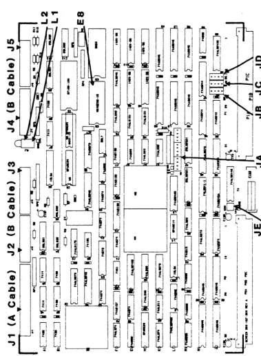
FIGURE 2-1. 712 - ~ LOCATIaq
xn.cx.;IQ) 712 Disk COntroller User I s Manual
2.2.1 EaSa
Address
Selection2.2.2
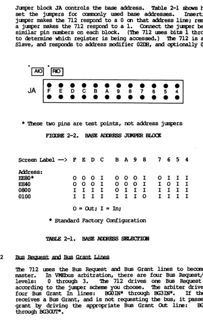
JlItIper block JA controls the base address. Table 2-1 shows h<7fI to set the j1.JtlPers for CXlIIOOllly used base addresses. Inserting a jlltlper makes the 712 respooo to a 0 a'l that address line; removing
a jlltlper makes the 712 respooo to a 1. Connect the ju:nper between
similar pin numbers on each block. ('!be 712 uses bits 1 through 3
to determine which register is being accessed.) '!be 712 is an Al6 Slave, and respoms to address modifier 02IE, and optionally 0298.
JA
•
F E D C• • •
• •
B A 9•
• •
8 7•
6 5 4• •
•
•
• •
•
•
•
•
•
• • •
*
'lbese two pins are test points, oot address jllOpersFIGlRE 2-2. BASE AIJ:mSS JUMPER BLOCK
Screen Label
-->
F E D C B A 9 8 7 6 5 hHress:EESO* 0 0 0 I 0 0 0 I 0 I I
EFAO 0 0 0 I 0 0 0 I I 0 I 0800 I I I I 0 I I I I I I
0100 I I I I I I I 0 I I I
o
=
Q.rt:; I=
In;* Standard Factory Configuration
TABLE
2-1 • BASE AIDmSS ~.Bus Request
.D1
Bua Grant Lines4
I
I
I I
'!be 712 uses the Bus Request
am
Bus Grant lines to becaoe 00s master. In VMEbus arbitration, there are four Bus Request/Grant levels: 0 through 3. 'lhe 712 drives one Bus Request line according to the jlltlper scheme you choose. ']he arbiter drives the four Bus Grant In lines: OOOIN* through OOJIN*. If the 712 receives a Bus Grant, and is not requesting the 00s, it passes thegrant by driving the appropriate Bus Grant Out line: OOOaJT* through BG3<lJT*.
[image:29.615.103.507.72.715.2]2.2.2
2.2.3
J3US ReQuest .and J3US Grant Lines (continued)
Select a request level by j\llp!ring one BusReq\lest (BRO* through BR3*), one Bus Grant In, and one Bus Grant QJt line to match the
selected request level. J1Il'Iper the remaining Bus Grant
In/0Ut
lines so that the incaning signal passes through the board (i.e., j1ll'lper BGxIN* to BGXOOT*, where x represents the remaining grant levels) •
For example, Figure 2-3 shCMS the jumpering scheme for level 0 (Figure 2-3A shows the jumper blocks as they actually a~ar on the board, 2-3B is labeled for this example): jOOlper JBl to JB5, then j\JllPer JCl to JC5, and JD1 to JOS. J\Ilp!r the remaining Grant levels fran JC6 to JD2, JCl to JD3, and JC8 to JD4. Factory configuration: Bus Request Level 3.
Sane VME processors only support Bus Request Level 3.
-0- -0- -0-
-1- -1- -1-
-2- -2- -2-
-3-BUS ROST BGOUT BG1N
~
1.---se
1-~1..---se
0It I' It
ae
1~~ ~.." -II 2
.II~ .II
se
3BR OUT IN
L BG--.J JB JC JO
Figure 2-3A. Actual Board Layout Figure 2-3B. Sample Jumpering Scheme
FIGORE 2-3. JtJMPERIK; BUS R8JU&ST AND BUS GRANT LE.VELS
Parallel Arbitration
If you are using the 712 in tarallel arbitration, and the Bus Grant OUt lines must be isolated fran the next slot's Bus Grant In Lines, remove all jumpers between JC 5-8 and JD 1-4 (See Figure 2-3B).
2.3 FORMAT PARAMETERS AND MAlNI'ENANCE IDOE IDCXaJT JUMPER
When jllIlper JE 1-2 is removed, you may only IOOdify format field lengths for fields 5 and 5A, and you may only execute the diagnostic portion of the Maintenance mode.
m.,cx;I03 712 Disk Controller User I s Manual
2.3 FORMAT PARAMETERS AND MAINl'tNANCE K>DE LOCI«lJT JUMH:R (continued) When jllOper JE 1-2 is installed, you may set all format plrcmeters
and have unrestricted use of the Maintenance mode.
'!be non-diagnostic portion of the Maintenance roode is proprietary to Xy10gics and subject to change without notice.
2.4 SELF TPST DISABLE
When jllOper JE 3-4 is installed, the 712 does not execute the Self Test on power-up.
2.5 PRCMS MID PALS
C6 B6
m.
L3
2.6 LIGHT EHI'l".rIR; DlOOES
180-002-151 181-001-022 181-001-023 181-001-024
'lYPE EPRCM
PAL PAL PAL
'!be 712 has two light emitting diodes (LEOs). IJ. (BSY) is the Busy LED (it is located closest to the printed circuit board). L2 (ERR)
is the Error LED (it straddles IJ.).
2.7 00ImD LABELS / m.vISlOO <lllmCL
All Xy10gics controllers use various revision control labels. 'Ibis information is iDportant when discussing configuration issues with us. Please familiarize yourself with your board revision levels before contacting us.
712-001-01
I
I
I
Product I I I
CrofiguratiOlL.-I l----Bevision Level
FlGORE 2-4. SMH.E PARr !UmER
'!be backplane of your systan ImlSt provide a VMEbus slot for the 712. '!be slot must be capable of handling a bus master, and the power
source
must handle the power constmption of the entire systan, including the 712.2.8.1
BacJwlane
.Jyng=trs2.8.2
Ranove any j\ltl}?ers that short, or cause the Interrupt:. Acknowledge (lACK IN/OOT) and lEA Grants (BG 0-3 IN/OOT) to bypass the slot in which you are installing the 712.
'!he card cage must have a slot at the proper ~ priority available for the 712. '!be 712 uses J:IttA to transfer data and IOPBs. Placement of the 712 in the :ttIA priority chain may be critical. '!he amount of bus bandwidth it uses will be high at tines; this may affect other boards in the systan. Likewise, other boards may not allow enough time for the 712 to J:IttA enough data to keep up with the disk; consider this when choosing a slot. If the 712 does not get a high enough priority, then its :ttIA falls behind what the disk requires, and it has to wait until the next revolution before continuing the transfer. If the 712 priority is high, it gets enough :ttIA time, but other boards having insufficient buffers may starve fran lack of :ttIA time. 'lhe priorities must be balanced for your system to work properly.
2.8.3 Power Considerations
'lhe 712 affects the power consl.lIlption of the entire canp.tter systen. 'lhe 712 uses +5 volts (4.75 to 5.25 volts) at 4.1 ClOpS. Be sure the power supplies can handle the entire power load. Readjust the voltages AFtER plugging in the 712. A power supply that is just adequate may cause intermittent and unusual problems
due to noise generated by occasionally going into OIIercurrent protection.
2.9 PREPARnI; '!HE DISK DRIVE FOR lNSl'ALLATlOO
Follow the manufacturer I s instructions for unpacking and inspecting
the disk drive.
Coofigure the drive for use with the 712. 'lbi.s entails setting up such parameters as the Unit Select and number of sectors per track. Consult the drive manual for the exact method of configuring your drive.
XYLOGICS 712 Disk COntroller User's Manual
2.9.1
2.9.2
Drive Dnit Select
A set of switches on one of the drive's internal circuit cards usually selects the drive Unit Number. ']he 712 accesses drives
with Unit Nurri:lers ranging fran 1 through 7. Set the first drive to Unit 1. ']he 712 adds one to the specified Unit Nunber because mDI drives do not sUR;X>rt Unit O. '!he 712 defaults to Unit O.
1U .IOm ~ WMRflR
o
1
2
.
.
6
pgySIC'AL DRIVE WMRBR
1
2 3
.
.
7
TABLE 2-3. 712 IOPB UNIT lIlMBERS
Ntmter ,gf Sectors .Per. Track
SWitches on one of the drive's internal circuit cards usually select the number of sectors ~r track. 'Jhe 7l2's overhead per sector varies fran drive to drive. To calculate the overhead for. the drive you are using, look. up the section on sector formats in your ESDI Drive Manual. For hard sector drives, the Sml of the
follOlrling bytes equals the 712 overhead:
Intersector Gap (ISG)
+
Blase Lock Oscillator (PLO) Sync+
.Ad3ress Sync + Address Field+
Address ORC+
Address Pad + (Gap 2+
Write Splice)+
rata PLO Sync+
rata Sync+
rata ECC+
rata Pad. .Ad3 your nuntler of data bytes ~r sector to the S\D of these bytes andyou will have the total sector size in bytes for your drive.
For soft sector drives, the Sml of the follOlrling bytes equals the
712 overhead:
ISG
+
Address Mark+
Pad+
PLO Sync+
Address Sync+
Address Field+
Address CRC+
1Iddress Pad+
Write Splice+
rata PLO Sync+
rata Sync+
rata ECC+
Data Pad+
Format Speed Tolerance Gap. Ml your number of data bytes ~r sector to the SlE of these byte