Composition and strain in thin Si
1−xGe
xvirtual substrates measured
by micro-Raman spectroscopy and x-ray diffraction
T. S. Perova,1,a兲J. Wasyluk,1K. Lyutovich,2E. Kasper,2M. Oehme,2K. Rode,3and A. Waldron1
1
Department of Electronic and Electrical Engineering, Trinity College, University of Dublin, Dublin 2, Ireland
2Institut für Halbleitertechnik, Universität Stuttgart, Pfaffenwaldring 47, 70569 Stuttgart, Germany 3School of Physics, CRANN, Trinity College, University of Dublin, Dublin 2, Ireland
共Received 18 August 2010; accepted 2 December 2010; published online 1 February 2011兲 Micro-Raman spectroscopy was employed for the determination of the germanium content, x and strain,, in ultrathin SiGe virtual substrates grown directly on Si by molecular beam epitaxy. The growth of highly relaxed SiGe layers was achieved by the introduction of point defects at a very low temperature during the initial stage of growth. SiGe virtual substrates with thicknesses in the range 40–200 nm with a high Ge content共up to 50%兲and degree of relaxation,r, in the range 20%–100% were investigated using micro-Raman spectroscopy and x-ray diffraction共XRD兲techniques. The Ge content, x, and strain,, were estimated from equations describing Si–Si, Si–Ge, and Ge–Ge Raman vibrational modes, modified in this study for application to thin SiGe layers. The alteration of the experimentally derived equations from previous studies was performed using independent data for x and r obtained from XRD reciprocal space maps. A number of samples consisting of a strained-silicon 共s-Si兲 layer deposited on a SiGe virtual substrate were also analyzed. The stress value for the s-Si varied from 0.54 to 2.75 GPa, depending on the Ge-content in the virtual substrates. These results are in good agreement with theoretically predicted values. © 2011 American Institute of Physics.关doi:10.1063/1.3536508兴
I. INTRODUCTION
Virtual substrates intended to be applied as global strain platforms for n-metal-oxide-semiconductor field-effect tran-sistors 共MOSFETs兲 consist of standard Si wafers with epi-taxially overgrown SiGe buffer layers. In SiGe buffer layers, a high Ge content and a high degree of relaxation are essen-tial because they provide the required strain in the Si channel as a quantum well for electrons. Strain relaxed buffers共SRB兲 are preferred to be thin for improved heat dissipation in MOSFETs, for better compatibility with devices of low di-mensions in integrated circuits, as well as for lower time and energy consumption during their production. Naturally, the quality of virtual substrates is very critical for the perfor-mance of the final device. The SRB must have a smooth surface morphology and low defect density. Lattice mis-match between Si and SiGe causes strain relaxation by the introduction of misfit dislocations in the interface plane and, especially, undesired threading dislocations in the bulk of the layers. The latter can be reduced by special additional mea-sures connected mostly with the growth of much thicker graded or constant composition layers, or with additional ex situ treatment.1–4Thus, SRB with small thickness, high Ge content, and high degree of relaxation is a rather ambitious aim. In order to lattice match SiGe buffer layers with the Si substrate, a controlled introduction of point defects at the beginning of SiGe buffer epitaxial growth, below the critical thickness, was proposed in Refs.5 and6. This can be real-ized by extreme reduction in growth temperature or by in
situ bombardment with Si+ ions available in the molecular beam epitaxy 共MBE兲chamber during the solid source MBE
共first stage of growth兲.7 During the next epitaxy stage at a medium growth temperature of typically 550 ° C, high point defect concentration should lead to the formation of pris-matic dislocation loops 共instead of dislocation arms thread-ing through the whole layers兲, and so promote the early re-laxation and lower threading dislocation density. The degree of relaxation can be adjusted by the choice of the very low temperature 共VLT兲step.
The industrial and research developments require me-trology solutions for the characterization and subsequent control of several important parameters in SiGe/Si and Si/ SiGe/Si structures such as the type and the magnitude of strain in the s-Si layer as well as the Ge content 共x兲 and relaxation factor共r兲in the SiGe buffers. Raman spectroscopy and x-ray diffraction 共XRD兲 are the only techniques which facilitate obtaining all the aforementioned parameters simul-taneously. We note that other techniques, which can be also used for the determination of x value, are Rutherford back-scattering spectrometry共RBS兲and secondary ion mass spec-trometry 共SIMS兲. However, RBS is not very accurate for measurements of thin films in a complicated structure, while SIMS is a destructive technique. XRD is quite accurate tech-nique 共in particular, when using advanced equipment with high resolution兲, but it requires a longer measurement time and is rarely utilized for in-line sample measurements. Therefore, the investigation of the application of Raman spectroscopy for accurate measurements of SiGe virtual sub-strates is of great importance.
Raman spectroscopy was applied widely for the investi-a兲Electronic mail: [email protected].
gation of composition and stress in Si/Ge structures such as SiGe epitaxial layers,8–14 Si/Ge superlattices,15–18and Ge/Si quantum wells and quantum dots.19,20For these structures the Ge content, x and strain,共orr兲can be obtained using three different methods of Raman data analysis. These are:共i兲 fre-quency method, using a set of the experimental equations obtained for the peak positions of the Si–Si, Si–Ge, and Ge–Ge modes, 共ii兲 intensity method, using the ratio of the integrated intensities of above mentioned modes, and finally
共iii兲using thin Si-cap layer 共or strained-silicon layer, s-Si兲, deposited on top of the SiGe, layer along with coherence conditions for these two layers. We note, that Raman inves-tigations were applied in the past to the analysis of compo-sition and strain of bulk SiGe,9,10 as well as to samples de-posited by different variations in the chemical-vapor deposition 共CVD兲techniques 共e.g., Ref.8兲and liquid-phase epitaxy.11 Quite recently micro-Raman technique was ap-plied to samples deposited by reduced pressure CVD 共Ref.
12兲 and plasma enhanced CVD.13,14 However, a very small number of works were devoted to micro-Raman investiga-tion of samples deposited by the MBE technique 共see Refs.
15–23兲, and most of these works were dealing with Si/Ge superlattices and quantum dots.17–23 It is worth noting that majority of the investigated SiGe samples had a thickness in the range from 300 to 4000 nm, and in addition to that these layers were deposited on top of step-graded or gradually graded Si1−xGexbuffer with x varied from 0 to the required value of x.
The main purpose of this work is to investigate the ap-plication of micro-Raman spectroscopy to very thin SiGe virtual substrates grown by the MBE technique. We also evaluate the validity of the existing equations, obtained for Raman data analysis, with the application to thin SiGe vir-tual substrates using independent evaluation of the Ge con-tent and strain from XRD data. Based on the results of the independent XRD measurements we first analyzed the set of equations for all three modes for fully relaxed samples. Tak-ing into account the contribution of strain to the shift in the phonon modes in SiGe layer the adjusted set of equations for the analysis of Raman data registered for any virtual SiGe substrate in the range of 0⬍x⬍0.5 was obtained. This en-abled us to use micro-Raman spectroscopy for the analysis of MBE grown, thin, virtual SiGe substrates, with a maximal deviation in the absolute value for Ge content, x, of⫾0.04, relative to XRD data. In addition to this, the strained Si layers grown on SiGe buffers were also investigated.
II. EXPERIMENTAL
A. Sample growth
For the growth of virtual substrates with ultrathin
共⬍100 nm兲SiGe buffer layers of high Ge content, a method using point defect supersaturation by a two-step growth pro-cedure in an MBE system is employed.5,6The first stage at a VLT 共135– 150 ° C兲 serves for the generation of point de-fects and their supersaturation in the growing layer. During the second stage, growth of an equal composition layer con-tinues at a conventional MBE temperature of 550 ° C. Here, point defects accumulated at the VLT stage may condense
and form dislocation loops which support the early relax-ation. Interaction of point defects with dislocations intro-duced during plastic strain relaxation can also improve the layer quality.24
Numerous samples, schematically shown in Fig. 1共a兲, are grown for the investigation of thin SiGe virtual substrates with Ge content ranging from 10 to ⬃50% as well as strained Si grown on top of some of these virtual substrates
关Fig.1共b兲兴. The epitaxial layers are grown with a solid source Si MBE equipment for 150 mm substrates.25Si was evapo-rated from an electron beam evaporator and Ge from a spe-cial effusion cell.26 The total thickness of the investigated SiGe buffer layer varies from 40 to 80 nm, including the VLT parts with thickness ranging from 20 nm to 30 nm, respectively共see Ref.6for details兲. For s-Si samples, above the SiGe buffer layer, a SiGe intermediate layer is grown which, among others things, may serve for quantum well doping and for spacer formation. In these series of samples, Ge content in the intermediate layers is the same as that of the SiGe buffer layer. The total thickness of the buffer layer combined with the intermediate layer does not exceed 200 nm. A 10–20 nm thick strained-Si layer is obtained at 500 ° C under conditions providing coherent growth of pseudomorphic layers 共sample parameters are given in TableI兲.
B. Raman measurements and analysis
1. Raman measurements
[image:2.612.316.557.52.152.2]Unpolarized Raman spectra were registered at room temperature in backscattering geometry using a RENISHAW 1000 Raman system equipped with a Leica micro-scope. Some additional measurements were also performed in Renishaw using a Micro-Raman inVia System. Data was registered at excitation wavelengths of Ar+ion laser at 514.5,
[image:2.612.316.559.674.755.2]FIG. 1. 共Color online兲Schematic of共a兲SiGe virtual substrate and共b兲of a strained-Si layer on an ultrathin SiGe buffer including a buried part with point defect supersaturation at low temperature initiating the early relaxation.
TABLE I. Nominal thickness and composition for samples with s-Si on SiGe virtual substrate关related to structures from Fig.1共b兲兴.
Sample name
Thickness of s-Si
共nm兲 SiGe layer composition
1797 20 Si0.88Ge0.12
1669 15 Si0.8Ge0.2
1799 12 Si0.7Ge0.3
488, and 457 nm and a 325 nm HeCd laser with inVia system for investigation of samples with s-Si. The thin SiGe layers are penetrated by visible light producing a Si substrate peak which is useful for calibration but also demands careful line analysis for extraction of nearby lines from SiGe. Laser light was focused on the sample through the ⫻50 magnification microscope objectives that provide a laser spot size in the range ⬃1 – 3 m. The scattered light from the sample was collected through the same microscope and directed through a spectrometer. It was then detected with a charge-coupled device. The laser power was kept between 3 and 10 mW to prevent samples heating and as a result causing an unwanted peak position shift. Before undertaking measurements the in-fluence of laser power on the linewidth and the peak position were checked on one of the samples from the series; the power was chosen at a level which did not affect the afore-mentioned spectra parameters. For the majority of samples, the data were collected at three to five different locations on the sample and no significant variance was observed, with average values well within experimental error limits.
Raman spectra registered from numerous samples, with x and rvarying from 0.1–0.5 and 20%–100%, respectively, were analyzed in order to accurately determine the peak po-sition, peak intensity and the linewidth of the phonon modes.
RENISHAW WIRE software allows Raman peaks to be fitted
with a variety of inbuilt functions for different peak shapes. To determine the Ge content and strain from the set of equa-tions for Si–Si, Si–Ge, and Ge–Ge vibrational modes 共as described in Sec. III A兲, the position of these peaks must be measured with a high accuracy. Two factors enable us to do so. A position of a Si–Si peak from the Si substrate was used as an internal reference for thin SiGe layers for visible exci-tation and a position of plasma line for UV exciexci-tation. All peaks from the SiGe layer were fitted with asymmetrical function,27while Si–Si peaks for s-Si and Si substrate were fitted by a Lorentzian function or by a mixture of Lorentzian and Gaussian functions.
2. Determination of peak position from experimental Raman spectrum
The major source of uncertainty in using frequency shifts to determine the composition and strain of a Si1−xGex buffer layers stems from the difficulty of accurately measur-ing the peak positions for Si–Si, Si–Ge, and Ge–Ge phonon modes. This is due to their asymmetry, large linewidth and small intensity, particularly for x⬍0.3.
For analysis of all three peaks associated with the SiGe layer an asymmetrical function was implemented 关see Eq.
共1兲兴into a user defined functions in ORIGIN. This allowed a better estimate to be made of the half width at half maximum
共HWHM兲of the spectrum, the intensity and the wave num-ber of an asymmetrical peak from the following equation:27
I共兲=1 2⫻
关1 − sign共−0兲兴⫻I0
冉
−0W1
冊
2+ 1 +1
2
⫻关1 − sign共0−兲兴⫻I0
冉
0−W2
冊
2+ 1
+1 2
⫻关1 − sign共−0兲兴⫻Ibkl+
1 2
⫻关1 − sign共0−兲兴⫻Ibkr, 共1兲
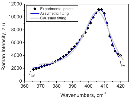
where0 is the peak position, I0 is the peak intensity,W is the HWHM at the lower frequency side 共W1兲 and at the higher frequency side共W2兲of the spectrum,Ibklis the
back-ground intensity on the lower frequency side of the curve, andIbkr is the background intensity on the higher frequency
side of the curve共see Fig.2兲. The function sign共−0兲turns to ⫺1 if 共−0兲 is negative and 1 if 共−0兲 is positive. Analysis of the peak positions proved to be considerably more accurate after the addition of these two terms. The asymmetrical function was found to fit the data better than the single Gaussian function共see example on Fig. 2兲or the set of standard Lorentzian and Gaussian functions. This was most notably in particular for the Si–Ge mode at higher Ge concentrations as the asymmetry of this band does increase with increasing Ge content. An example of choosing values for theIbklandIbkrpoints used in Eq.共1兲is shown in Fig.2,
in order to best fit the Si–Ge band obtained from a particular example at x = 0.35.
C. XRD measurements
For high resolution XRD 共HRXRD兲 measurements the BRUKER D8 Discovery with a primary beam channel cut Ge 共110兲crystal monochromator, producing an intense, par-allel CuK␣1 monochromatic beam 共with wavelength = 1.5406 Å兲, was used. The secondary beam was equipped with a LynxEye 1D detector allowing for fast mapping of the reciprocal space. The sample lattice parameters were deter-mined by measuring reciprocal space maps 共RSMs兲 around the Si 关113兴 reflection and estimating the thin film lattice
360 370 380 390 400 410 420
0 2000 4000 6000 8000 10000 12000
I bkr Experimental points
Assymetric fitting Gaussian fitting
R
aman
Inten
si
ty,
a.u.
[image:3.612.332.538.47.203.2]Wavenumbers, cm-1 Ibkl
FIG. 2. 共Color online兲Fitting of Ge–Ge band with asymmetrical关Eq.共1兲兴
and Gaussian functions. The example of the best choice forIbkl and Ibkr
parameters from the relative separation in ⍀ and 2. For sample 940 RSMs were also registered around Si 关224兴 re-flection; the obtained results were similar to Si关113兴 reflec-tion. Strain and Ge concentration were then obtained by as-suming the lattice expansion due to the Ge content obeying Dismukes28model.
III. RESULTS AND DISCUSSIONS
A. Frequency method
1. Equations for fully relaxed SiGe layers
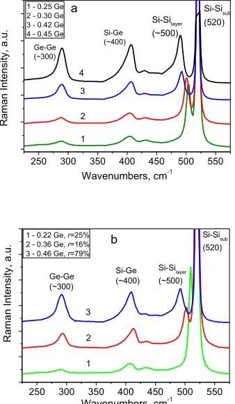
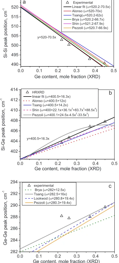
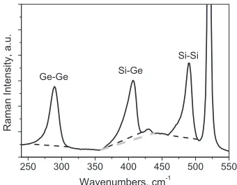
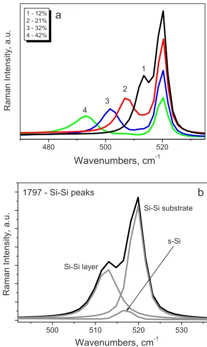
The Raman spectrum of a strained SiGe heterostructure alloy consists of three distinct peaks whose energies 共and therefore the peak positions兲 depend on the x 共Ge content兲 and the strain.9,10,18The three strong first-order lines shown in Fig.3 in Raman spectra of a few SiGe virtual substrates are due to the atomic vibrations of Si–Si 共at ⬃502 cm−1兲, Si–Ge共at⬃405 cm−1兲and Ge–Ge共at⬃290 cm−1兲bonds in the SiGe alloy. The Raman spectra for SiGe virtual substrates with different Ge content and with nearly the same high re-laxation factor共r⬎93%兲, i.e., for fully relaxed samples, are presented in Fig.3共a兲. It can be seen from this figure that the position of all three peaks are shifted with respect to each other depending on x.
The spectra obtained for samples with different compo-sition and relaxation factor 共or strain兲, shown in Fig. 3共b兲, demonstrate a quite substantial shift in all three modes from their position for fully relaxed samples. As can be seen from Fig.3共b兲the position of all three bands is changed depending on x and. The values of x andcan be estimated from a set
of equations suggested in the literature for bulk SiGe or rela-tively thick SiGe layers grown by the CVD technique. This includes the bulk materials, obtained by powder compression,10 single crystal SiGe alloy grown by liquid-phase epitaxy11as well as SiGe layers deposited by different CVD methods of deposition on graded SiGe layers or di-rectly onto a Si substrate. For the Si–Si peak position,SS, of
a SiGe layer the following experimental equations are intro-duced
SS共x兲= 520 − 70x 关11兴, 共2a兲
SS共x兲= 520.2 − 62x 关8,10兴, 共2b兲
SS共x兲= 521.2 − 67.9x 关19兴, 共2c兲
SS共x兲= 520.7 − 66.9x 关14兴. 共2d兲
Equations 共2a兲–共2c兲 are valid mainly in the region of Ge content 0⬍x⬍0.5, while Eq. 共2d兲 is obtained for the wide range of x. The following equations are used for Si–Ge peak position,SG
SG= 400.5 + 14.2x 关8兴, 共3a兲
SG= 400.5 + 12x 关11兴, 共3b兲
in the range of 0⬍x⬍0.5 and for 0⬍x⬍1 the following expressions are used
SG= 400 + 22.07x − 36.14x2+ 83.73x3
− 88.54x4 关19兴, 共3c兲
SG= 400.1 + 24.5x − 4.5x2− 33.5x3 关14兴. 共3d兲
The experimentally measured dependences of the Ge–Ge phonon frequency,GG, on x are described by the equations
GG= 282.5 + 16x 关8兴, 共4a兲
GG= 280.8 + 19.37x 关17兴, 共4b兲
GG= 280.3 + 19.4x 关14兴. 共4c兲
In order to determine the optimal set of expressions suitable for our samples we select a number of samples with different Ge content and with relaxation factor close to 100%. The Ge content for these samples is obtained by XRD and the Ra-man peak position is corrected for the small residual strain determined from the relaxation degree 共TableII兲
= −f共1 −r兲, 共5兲
with as a strain, f as a lattice mismatch, andr as a strain relaxation. Strain and mismatch have different signs as com-pressive strain is defined as negative in elasticity theory. fis a parabolic function of the Ge content, x, when slight devia-tion from Vegard’s law 共linear interpolation between Si and Ge兲 is taken into account as given by Dismukes28 for the bulk SiGe. This equation was confirmed later for epitaxial layers29
250 300 350 400 450 500 550
R
aman
In
tens
ity,
a.u.
Wavenumbers, cm-1 1 - 0.25 Ge
2 - 0.30 Ge 3 - 0.42 Ge 4 - 0.45 Ge
Si-Sisub (520) Si-Silayer
(~500)
Si-Ge (~400) Ge-Ge
(~300)
1 2 3 4
a
250 300 350 400 450 500 550
2 3
Ge-Ge (~300)
Si-Ge (~400)
Si-Silayer (~500)
Si-Sisub (520)
Raman
Intensity
,a
.u.
Wavenumbers, cm-1 1 - 0.22 Ge,r=25%
2 - 0.36 Ge,r=16% 3 - 0.46 Ge,r=79%
1
[image:4.612.90.259.50.340.2]b
FIG. 3. 共Color online兲 共a兲 Raman spectra for SiGe/Si samples with r
f共SiGe兲= 0.02 0.5431x +
0.0026 0.5431x
2. 共6兲
The relaxation degree r of the selected samples varies be-tween 92% and 104%. The values larger than 1 stem from a small tensile strain originating from thermal mismatch of completely relaxed SiGe layers cooled down to room tem-perature. The correction of the Raman peak position for strain is performed using the literature values8,30–32 of strain phonon coefficients −830 cm−1, −575 cm−1, and −384 cm−1 for Si–Si, Si–Ge, and Ge–Ge bands, respectively. The accu-rate values of these literature strain-phonon coefficients are not critical, because of the only small correction needed for the selected samples. The results are shown in Fig.4.
2. Equations for fully relaxed SiGe layers
The peak position obtained for all three Raman modes after the fitting with asymmetrical function are plotted in Fig.
4against values of x, determined from XRD measurements. The linear curves obtained from Eqs.共2a兲–共2d兲on the depen-dence of Si–Si peak position versus Ge content are shown in Fig.4共a兲together with Raman and XRD experimental data. The same set of data and linear and nonlinear dependences are shown in Fig.4共b兲for Si–Ge and in Fig.4共c兲for Ge–Ge modes.
As can be seen from Fig.4共a兲, the best fit to XRD data results in the linear equation
SS= 520 − 70.5s, 共7兲
which is quite close to the equation obtained in Ref.11, see Eq.共2a兲.
Figure4共b兲shows a similar set of data for peak position of Si–Ge mode versus x obtained from XRD data. In this case, the experimental data obtained for our set of samples significantly deviate from the linear and nonlinear
dependen-cies described by Eqs.共3a兲and共3b兲and Eqs.共3c兲and共3d兲. The best fit to obtained experimental data results in the fol-lowing linear equation for 0⬍x⬍0.5:
SG= 400.5 + 16x. 共8兲
As can be seen from Fig. 4共c兲a significant deviation of the experimental data points from all curves is observed for the Ge–Ge peak position versus x. This confirms previously made conclusions,8that it is more difficult to use the Ge–Ge peak for the extraction of information on x from Raman data, particularly for thin SiGe layers with x⬍0.4. For consistency we will analyze our experimental results for all three peaks described above, using Eq. 共4a兲 obtained in Ref. 8 for a Ge–Ge peak. However, most of the data analysis was done based on Eqs.共7兲and共8兲.
3. Equations for strained SiGe layers
The next step is to determine the set of equations for strained SiGe virtual substrate with relaxation factor ⬍100%. For this purpose, the additional terms accounting for strain in Eqs.共4a兲,共7兲, and共8兲were used.8This results in the following set of equations describing the peak position of SiGe layer under strain
SS= 520 − 70.5x − 830, 共9兲
SG= 400.5 + 16x − 575, 共10兲
GG= 282.5 + 16x − 384. 共11兲
From Eqs.共9兲and共10兲, we obtain the following expressions for x andcalculations:
x =共SG− 400.5兲− 0.6928⫻共SS− 520兲
[image:5.612.123.486.73.301.2]64.84 , 共12兲
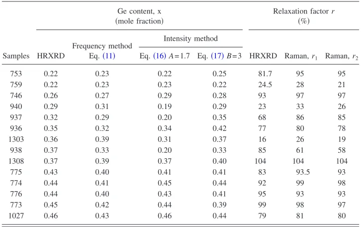
TABLE II. The calculated Ge concentration and relaxation factor for samples measured by XRD and Raman techniques关related to structures from Fig.1共a兲兴.
Samples
Ge content, x 共mole fraction兲
Relaxation factorr 共%兲
HRXRD
Frequency method Eq.共11兲
Intensity method
HRXRD Raman,r1 Raman,r2
Eq.共16兲A= 1.7 Eq.共17兲B= 3
753 0.22 0.23 0.22 0.25 81.7 95 95
759 0.22 0.23 0.23 0.22 24.5 28 21
746 0.26 0.27 0.29 0.28 93 97 97
940 0.29 0.31 0.19 0.29 23 33 26
937 0.32 0.29 0.20 0.35 68 86 85
936 0.35 0.32 0.34 0.42 77 80 78
1303 0.36 0.39 0.31 0.37 16 26 19
938 0.37 0.33 0.20 0.33 85 61 58
1308 0.37 0.39 0.37 0.40 104 104 104
775 0.43 0.40 0.41 0.41 83 93.5 93
774 0.44 0.41 0.45 0.44 92 99 98
776 0.44 0.40 0.43 0.41 95 93 93
773 0.45 0.42 0.44 0.39 99 98 97
SiGe=520 −SS− 70.5x
830 . 共13兲
The results of calculations of x and using Eqs. 共12兲 and
共13兲 enable us to process the Raman data obtained for the numerous samples investigated in this work, with x in the range 0 to 0.5 and for the relaxation factor in the range 20%–100%.
The following relationships, describing the shift in the peak positions for all three modes for fully strained layers, were obtained based on Eqs.共9兲–共11兲and assuming for sim-plicity a linear relationship共Vegard’s law兲between Ge con-tent and strain:
⌬SS= 36x, ⌬SG= 40x, and ⌬GG= 32x. 共14兲
The degree of relaxation,rin a SiGe layer on a Si substrate can be obtained using the experimental Raman shift in the
Si–Si peak ⌬exp from the unstrained peak position for a Si substrate at 520 cm−1from the following expression:15,33
r1=
⌬exp−⌬s
⌬r−⌬s
⫻100%, 共15兲
where⌬r= 70.5x and ⌬s= 36x are Raman shifts in the fully
relaxed and the fully strained epilayers from the bulk Si, respectively. In addition, the r values were also calculated from the expression共5兲and these are denoted asr2in Table
II.
The results, shown in Figs. 5共a兲–5共c兲, demonstrate dis-tribution of the obtained data between two linear dependen-cies of phonon frequendependen-cies versus x, obtained for the fully strained and fully relaxed SiGe virtual substrates. It can be
0.0 0.1 0.2 0.3 0.4 0.5
490 495 500 505 510 515 520 525 y=520-70.5x Experimental Linear fit (ω=520.2-70.5x) Alonso (ω=520-70x) Tsang(ω=520.2-62x) Brya (ω=520.2-66.7x) Shin (ω=521.2-67.9x) Pezzoli (ω=520.7-66.9x)
Si -Si p eak posi tion, c m -1
Ge content, mole fraction (XRD) a
0.0 0.1 0.2 0.3 0.4 0.5
402 404 406 408 410 412 414 Si-Ge peak positio n, cm -1 y=400.5+16.3x
Ge content, mole fraction (XRD) HRXRD
linear fit (ω=400.5+16.3x) Alonso (ω=400.5+12x) Tsang (ω=400.5+14.2x) Shin (ω=400+22.1x+36.1x2
+83.7x3 +88.5x4
) Pezzoli (ω=400.1+24.5x-4.5x2
-33.5x3 )
b
0.0 0.1 0.2 0.3 0.4 0.5
282 284 286 288 290 292 294 Ge-G e p e a k p o s itio n, cm -1
Ge content, mole fraction (XRD) experimental
Brya (ω=282+12.5x) Tsang (ω=282.5+16x) Lookwod (ω=280.8+19.4x) Pezzoli (ω=280.3+19.4x)
[image:6.612.333.540.43.520.2]c
FIG. 4. 共Color online兲 共a兲Si–Si,共b兲Si–Ge, and 共c兲Ge–Ge Raman peak position vs Ge content determined by HRXRD.
0.0 0.1 0.2 0.3 0.4 0.5
-30 -25 -20 -15 -10 -5 0 Raman Fully Relaxed Fully Strained Δω Si-Si ,c m -1
Ge content, mole fraction (Raman) a
0.0 0.1 0.2 0.3 0.4 0.5
0 2 4 6 8 10 12 14
Ge content, mole fraction (Raman)
Δω Si-G e ,c m -1 Raman Fully Relaxed Fully Strained b
0.0 0.1 0.2 0.3 0.4 0.5
0 4 8 12 16 20
Ge content, mole fraction (Raman)
[image:6.612.71.277.56.511.2]Δω Ge-Ge ,c m -1 Raman Fully Relaxed Fully Strained c
seen that the obtained data are within the range of data pos-sible for different values of x for the investigated samples. A small deviation of experimental data from the fully strained curve for Ge–Ge mode is observed; this is due to the diffi-culties of Ge–Ge peak analysis for samples with small Ge content. The results of comparing data obtained from XRD and Raman techniques for the relaxation factor and Ge con-tent are summarized in TableII. We can see that the devia-tion of the values obtained by Raman spectroscopy for the relaxation factor for some samples, for example for samples 940, 937, and 938, is larger than that obtained for the x value
共this will be discussed in Sec. III B兲. Figure 6demonstrates the difference between the x values obtained from Raman
共xRaman兲and XRD共xXRD兲measurements versus Ge content. We can see that the maximal deviation of x values estimated from Raman data are within ⫾0.04 relatively to XRD data. Bearing in mind the difficulties with analysis of data for very thin layers we believe that the obtained results demonstrate the usefulness of micro-Raman spectroscopy for the determi-nation of Ge content and strain 共or degree of relaxation兲 in thin SiGe layers.
B. Intensity method
Let us now analyze the second approach for the deter-mination of composition in SiGe alloy using Raman spec-troscopy. The methods suggested in Refs. 8, 9, and 34 are based on the comparison of the relative intensities of the first order Si–Si, Si–Ge, and Ge–Ge bands. The ratios of the in-tegrated intensities of three main modes can be related in the first-order approximation to the number of nearest neighbor bonds and, therefore, are the functions of the Ge content in the alloy. According to a simple statistical model, the relative intensities are roughly proportional to the relative numbers of corresponding bonds types, i.e., 共1 − x兲2, x2, and 2x共1 − x兲for the Si–Si, Ge–Ge, and Si–Ge modes, respectively.9
The major advantage of using the intensity method is that there is no need for highly accurate fitting of the phonon bands, which is extremely important for the frequency method described in Sec. III A 3. The determination of alloy composition using the intensity of the modes is also indepen-dent of whether the layer is strained or relaxed. However, the
intensities of the Si–Ge and Ge–Ge modes depend strongly on the methods used to measure them. In particular, there is some uncertainty about the determination of the baseline for each particular band shown in Fig.7. This problem is espe-cially pertinent for the Si–Ge mode as there are significant peaks on the high energy side of the main mode. These have been attributed to localized Si–Si motion in the neighbor-hood of one or more Ge atoms.9,10,18As was stated in Ref.
34, the localized Si–Si peaks were included in the measure-ment of integrated intensity of the Si–Ge mode. In this in-vestigation, the intensity of the Si–Ge mode was measured excluding the peaks at 430 and ⬃450 cm−1 and the area of the Ge–Ge peak was estimated by excluding the long wings on both sides of the curve共see black dashed baseline in Fig.
7兲. The intensity of Si–Si mode was measured by fitting a single peak from SiGe layer共truncated in the wave number region as shown in Fig.7兲when this peak is well separated from Si–Si peak of Si substrate. If two Si–Si peaks were in close proximity, the simultaneous fitting of both peaks was performed with mixture of Lorentzian and Gaussian func-tions.
Assuming random mixing in the alloy, the relative inte-grated intensities of the modes are expected to vary with the Ge mole fraction as follows:34
I共Si – Si兲 I共Si – Ge兲=
A共1 − x兲
2x 共16兲
and I共Ge – Ge兲 I共Si – Ge兲 =
Bx
2共1 − x兲. 共17兲
Because of resonance effects, the intensities of the various modes vary with the wavelength of the exciting light, as does the optical system. Thus, coefficientsAandBmust be deter-mined experimentally for each wavelength. A and B were determined for our experimental setup for 457 nm excitation wavelength using the XRD data available for a number of samples as described above.
The integrated intensities of phonon modes were calcu-lated by using theRENISHAW WIREpeak profile analysis soft-ware. Using x values, measured by XRD, the relative inten-sities for the investigated samples are plotted versus Ge content in Figs. 8共a兲 and 8共b兲. As can be seen from both figures the best fitting of experimental data is obtained at A
0.1 0.2 0.3 0.4 0.5
-0.08 -0.04 0.00 0.04 0.08
xRama
n
-xXR
D
,m
ol
e
fra
ct
ion
[image:7.612.350.520.47.180.2]Ge content, mole fraction (XRD)
FIG. 6. 共Color online兲Deviation of Ge content obtained from Raman and XRD data 共xRaman− xHRXRD兲 vs Ge content determined by HRXRD measurements.
250 300 350 400 450 500 550
Si-Si Si-Ge
R
ama
n
Int
en
si
ty,
a.u
.
[image:7.612.68.279.49.199.2]Wavenumbers, cm-1 Ge-Ge
= 1.7 andB= 3.0. By comparing Figs.8共a兲and8共b兲, it seems that better correlation between Raman and XRD results is achieved with Eq. 共16兲. This is not surprising bearing in mind that the Ge–Ge peak for a thin SiGe layer is quite weak, in particular for small x.
As can be seen from TableII, the intensity method en-ables the determination of x to an accuracy of ⫾0.05 using Eq.共16兲. As was mentioned above, considerable uncertainty exists as to where the baseline of a peak begins and where it ends. Mooney et al.34 found the integrated intensities ratios to be in good agreement with Eqs.共16兲and共17兲only if the peak at 430 cm−1 is included in the intensity of the Si–Ge mode, while in this work all local Si–Si peaks were excluded from the calculation of ISi–Ge and ISi–Si. When these peaks were included, the accuracy of the estimation of x was re-duced to⫾0.08. Interestingly, for the samples 940, 937, and 938 described in Sec. III A 3 a significant deviation between x values obtained by XRD and from Raman intensity method using Eq. 共16兲 was obtained. However, using Eq. 共17兲 the results obtained for x are quite close to the XRD data. In order to allow explanation of this observation, further experi-mental investigations are necessary.
C. Strained Si on SiGe virtual substrate
The main feature of the Raman spectra of strained-Si on ultrathin SiGe substrates obtained with visible excitation light is the presence of three Si–Si peaks in the region
⬃530– 490 cm−1共see Figs.9and10兲. These are the peak at
520 cm−1, which corresponds to the Si substrate, the peak at
⬃510– 518 cm−1 which is assigned to strained Si and the peak in the range ⬃490– 510 cm−1 which belongs to the Si–Si mode in the SiGe layer. Depending on the Ge content and strain in the underlying SiGe virtual substrate, these three peaks can be either quite well separated or very close together. This situation is quite different from the case of Raman spectra of strained Si on thick SiGe substrates where the peak at 520 cm−1 is not observed due to the limited depth of laser light penetration into the SiGe layer.15,35In this case the Si–Si peak arising from the Si substrate can be used with high accuracy as an internal reference in analyzing the Raman spectrum. The intensity of a peak at 520 cm−1 is much larger compared to the two other Si–Si peaks in the case of a thin s-Si layer on an ultrathin SiGe layer and, in particular, in comparison with the peak for s-Si, due to its small thickness 关see Fig. 1共b兲兴. This requires very careful analysis of the Raman spectra in the range 490– 530 cm−1.36
Raman spectra for the four samples, registered at 514.5 nm excitation, are shown in Fig.9共a兲. For the sample 1797 with low Ge content共⬃10%兲there is no visible sign of the Si–Si peak from s-Si, while for the samples with higher Ge con-tent, a small shoulder or small bump related to this peak can be seen in between the two peaks at 520 and at
0.1 0.2 0.3 0.4 0.5 0.6
0 2 4 6
8 A(1-x)/2x A=1.85I(Si-Si)/I(Si-Ge)
A(1-x)/2x A=1.7
I(Si-S
i)
/I(Si-Ge)
Ge content, mole fraction (XRD)
a
0.1 0.2 0.3 0.4 0.5 0.6
0.0 0.5 1.0 1.5 2.0
2.5 I(Ge-Ge)/I(Si-Ge)Bx/(2*(1-x)) B=3.2
Bx/(2*(1-x)) B=3
I (Ge
-Ge
)
/I (Si-Ge)
Ge content, mole fraction (XRD)
[image:8.612.332.537.46.390.2]b
FIG. 8. Intensities ratio vs Ge content, x from the experimental data共 sym-bols兲and共a兲from Eq.共16兲atA= 1.85共gray line兲andA= 1.7共black line兲and 共b兲from Eq.共17兲atB= 3.2共gray line兲andB= 3共black line兲.
480 500 520
R
aman
Inten
si
ty
,a
.u
.
4 3 2
a
1 - 12% 2 - 21% 3 - 32% 4 - 42%Wavenumbers, cm-1
1
500 510 520 530
Si-Si layer
Si-Si substrate
s-Si 1797 - Si-Si peaks
Raman
Intensity,
a.
u.
Wavenumbers, cm-1
[image:8.612.70.272.49.353.2]b
FIG. 9. 共Color online兲 共a兲Raman spectra of sample 1797, 1669, 1799, and 1800 with increasing Ge content collected at 514 nm excitation wavelength. The strained-Si peak is observed between the Si substrate peak at 520 cm−1
⬃490– 512 cm−1. By fitting the Raman spectrum with three Lorentzian functions, all three peaks are revealed as shown, for example, in Fig.9共b兲. The results obtained for the shift, ⌬, of Si–Si peak from the unstressed Si–Si peak at 520 cm−1for all analyzed samples are summarized in Table
III along with data obtained using 488 and 325 nm excita-tions. For UV excitation, a simultaneous recording of the plasma line was used as the internal reference, because the Si–Si peak from the substrate does not show up in Raman spectrum for the shorter excitation wavelength. The values of Raman peak shift, ⌬, obtained with all three excitation wavelengths are in good agreement 共see TableIII兲. The ob-tained results demonstrate that visible light Raman spectros-copy can be reliably used for the characterization of strained Si on ultrathin SiGe virtual substrates. However, careful fit-ting of the spectra is required in this case for proper data analysis.
By measuring the shift in the Raman peak position,⌬, obtained for the s-Si layer, the magnitude of stress, , and strain, , can be estimated by using a simple equation, de-scribing the biaxial stress in a Si lattice30,32
Si=⌬/c 共18兲
withc= 4.61⫻10−9共Pa cm−1兲,
Si共%兲=
冉
⌬b
冊
⫻100% =aSistrain−aSi
aSi ⫻100%, 共19兲
whereb is the strain-phonon coefficient, which was taken as 830 cm−1, aSi andaSi
strain
are the lattice constants of relaxed and strained Si, respectively. The values of Si and Si are related to the elastic constants as
Si= Ef
1 −vf
⫻ Si 共20兲
for biaxial stress. Here Ef is Young’s modulus for the film andfis Poisson’s ratio of the film. Taking the values ofEf andf as 130.2 GPa and 0.28, respectively,37,38we conclude that the phonon coefficient ratio b/c should be b/c=Ef/共1 −f兲= 180.5 GPa. The selected coefficientscandbobtained from the literature fit this relationship very well. The strain values thus obtained were compared with the data estimated for Sifrom analysis of the spectral shifts in the Si–Si pho-non band registered from the SiGe layers, taking into ac-count the coherence conditions
aSiGestrain=aSistrain. 共21兲
By analogy with the Eq. 共19兲 and taking into account Eq.
共21兲and that
aSiGestrain=aSiGerel 共x兲共1 +SiGe兲,
where aSiGerel 共x兲 can be determined from Dismukes model,28 we obtain
Si共%兲=aSiGe strain−a
Si aSi
⫻100%. 共22兲
The results obtained forSi共%兲estimated form Eqs.共19兲and
共22兲are presented in TablesIIIandIValong with values obtained from Eq. 共18兲. Both series of results for Si共%兲 show very good agreement. We believe that this agreement indicates that the results, obtained from the analysis of com-plicated Raman spectra in Si–Si mode region under visible excitation, allows us to obtain reliable data on stress in strained Si layers on SiGe virtual substrates. The calculations of the Ge content 共x兲 and strain SiGe were performed by means of simultaneous measurements of theSSandSGfor the underlying SiGe layer, followed by calculations using the pair of Eqs.共12兲 and共13兲. The relaxation factor for a SiGe layer was also estimated from Eq.共15兲. The values x,, and
480 500 520
3 2
s-Si 488 nm excitation
Si-Si peak
1 - 1797 2 - 1669 3 - 1799
R
aman
In
ten
sit
y,
a.u.
Wavenumbers, cm-1
1 a
480 520 560
1 2
3 1 - 1800
2 - 1799 3 - 1797 4 - Si-ref. 325 nm excitation
Si-Si peak
Raman
Intensity,
a.u.
Wavenumbers, cm-1
b
[image:9.612.89.257.49.333.2]4
FIG. 10. 共Color online兲Raman spectra for samples 1797, 1669, and 1799 collected at共a兲488 nm excitation and共b兲at 325 nm excitation wavelength.
TABLE III. Shift in Si–Si peak共⌬兲, stress, and strain for s-Si layer obtained from Raman spectra at different excitation wavelengths关related to structures from Fig.1共b兲兴.
Sample name
Raman shift in Si–Si band,⌬ 共cm−1兲
关Eq.共18兲兴
共GPa兲 Si⫻100%共Eq.共19兲
514 nm 488 nm 325 nm
1797 2.49 2.66 2.56 0.54 0.3
1669 5.3 ¯ ¯ 1.13 0.63
1799 7.24 7.3 7.0 1.57 0.87
[image:9.612.126.485.657.756.2]r determined from analysis of Raman spectra are in good agreement with XRD data.
Conversely, using the coherence conditions, the analysis of the Si–Si peak for s-Si layer enables us to independently evaluate the value of Ge content and strain in SiGe. The obtained results are in very good agreement with Raman analysis of SiGe bands, which supports the use of the modi-fied Eqs. 共9兲 and共10兲for the simultaneous calculation of x andSiGein thin virtual SiGe substrates. This agreement also shows that the results obtained from the analysis of compli-cated Raman spectra in the Si–Si mode region allows us to provide reliable data on stress in strained Si layers on SiGe virtual substrates.
IV. CONCLUSION
The Ge content, x, and the relaxation factor,r, in thin SiGe layers were calculated using a set of equations for Si– Si, Si–Ge, and Ge–Ge Raman vibrational modes, adapted in this work for use with thin SiGe layers. The alterations to the equations were done using independent measurements of x and r, obtained from XRD and Raman measurements for fully relaxed SiGe virtual substrates.
It was shown that by using the ratios of the integrated intensities of Si–Si, Si–Ge, and Ge–Ge phonon modes for SiGe virtual substrates, values for x can be determined which are in reasonable agreement with XRD and Raman Fre-quency methods. The intensity method provides the addi-tional advantage of allowing the use of the Ge–Ge peak for x⬍0.3, while the more elaborate frequency method uses only the Si–Si and Si–Ge peaks. Based on the results dis-cussed in this paper we conclude that for more reliable Ra-man analysis of thin SiGe layers both methods should be used.
Finally, visible micro-Raman spectroscopy is demon-strated to be a reliable tool for the characterization of com-position and strain in ultrathin SiGe virtual substrates, as well as for strained Si, by careful fitting of the spectra. Al-though the accuracy of the XRD technique is higher
共⬍⫾1% for the determination of the Ge content兲than Ra-man spectroscopy共⫾4%–10%兲, the latter technique is much faster. Raman spectroscopy also allows probing of the samples at different depths as well as in-line measurements. Finally, the method also enables local measurements to be taken from microstructured devices.
ACKNOWLEDGMENTS
J. Wasyluk would like to acknowledge the financial sup-port of IRCSET Ireland, Postgraduate Award and ICGEE, Ireland Bursary Award. We acknowledge the financial sup-port from EU network of excellence NanoSil as well as from the Centre for Research on Adaptive Nanostructures and Nanodevices 共CRANN兲 and Science Foundation Ireland
共Project 08/CE/I1432兲. T. Smith共Renishaw兲and R. Mathieu are thanked for help with Raman experiments.
1E. A. Fitzgerald, M. T. Curie, S. B. Samavedam, T. A. Langdo, G.
Tara-schi, V. Yang, C. W. Leitz, and M. T. Bulsara,Phys. Status Solidi A171, 227共1999兲.
2B. Holländer, S. Mantl, R. Liedtke, S. Mesters, H.-J. Herzog, H. Kibbel,
and T. Hackbarth,Nucl. Instrum. Methods Phys. Res. B148, 200共1999兲.
3Z. Yang, J. Alperin, W. I. Wang, S. S. Lyer, T. S. Kuan, and F. Senemdy, J. Vac. Sci. Technol. B16, 1489共1998兲.
4I. Berbezier and A. Ronda,Surf. Sci. Rep.64, 47共2009兲.
5E. Kasper, K. Lyutovich, M. Bauer, and M. Oehme,Thin Solid Films336,
319共1998兲.
6K. Lyutovich, E. Kasper, F. Ernst, M. Bauer, and M. Oehme,Mater. Sci. Eng., B71, 14共2000兲.
7M. Bauer, M. Oehme, K. Lyutovich, and E. Kasper,Thin Solid Films336,
104共1998兲.
8J. C. Tsang, P. M. Mooney, F. Dacol, and J. O. Chu,J. Appl. Phys.75,
8098共1994兲.
9M. A. Renucci, J. B. Renucci, and M. Cardona, inLight Scattering in
Solids, edited by M. Balkanski 共Flammarion Sciences, Paris, 1971兲, p.
326.
10W. J. Brya,Solid State Commun.12, 253共1973兲.
11M. I. Alonso and K. Winer,Phys. Rev. B39, 10056共1989兲.
12J. M. Hartmann, B. Gallas, J. Zhang, and J. J. Harris, Semicond. Sci. Technol.15, 370共2000兲; J. M. Hartmann, Y. Bogumilowicz, P. Holliger, F. Laugier, R. Truche, G. Rolland, M. N. Séméria, V. Renard, E. B. Olsha-netsky, O. Estibals, Z. D. Kvon, J. C. Portal, L. Vincent, F. Cristiano, and A. Claverie,ibid.19, 311共2004兲; M. Mermoux, A. Crisci, F. Baillet, V. Destefanis, D. Rouchon, A. M. Papon, and J. M. Hartmann,J. Appl. Phys.
107, 013512共2010兲.
13F. Pezzoli, E. Grilli, M. Guzzi, S. Sanguinetti, D. Chrastina, G. Isella, H.
von Känel, E. Wintersberger, J. Stangl, and G. Bauer,Mater. Sci. Semi-cond. Process.9, 541共2006兲.
14F. Pezzoli, E. Bonera, E. Grilli, M. Guzzi, S. Sanguinetti, D. Chrastina, G.
Isella, H. Von Känel, E. Wintersberger, J. Stangl, and G. Bauer,Mater. Sci. Semicond. Process.11, 279共2008兲.
15B. Dietrich, E. Bugiel, J. Klatt, G. Lippert, T. Morgensten, H. J. Osten, and
P. Zaumseil,J. Appl. Phys.74, 3177共1993兲.
16S. Rath, M. L. Hsieh, P. Etchegoin, and R. A. Stradling,Semicond. Sci. Technol.18, 566共2003兲.
17J. C. Bean,Science230, 127共1985兲.
18F. Cerdeira, A. Pinczuk, and J. C. Bean,Phys. Rev. B31, 1202共1985兲. 19H. K. Shin, D. J. Lockwood, and J. M. Baribeau,Solid State Commun.
114, 505共2000兲.
20H. Brugger, G. Abstreiter, H. Jorke, H. J. Herzog, and E. Kasper,Phys. Rev. B33, 5928共1986兲.
21P. H. Tan, D. Bougeard, G. Abstreiter, and K. Brunner,J. Appl. Phys.98,
[image:10.612.124.486.75.175.2]113517共2005兲.
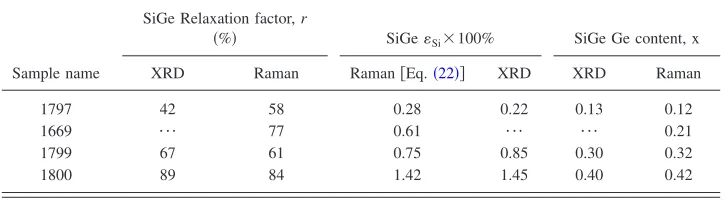
TABLE IV. Ge content, relaxation factor, and strain in SiGe layers obtained from XRD and Raman measure-ments关related to structures from Fig.1共b兲兴.
Sample name
SiGe Relaxation factor,r
共%兲 SiGeSi⫻100% SiGe Ge content, x
XRD Raman Raman关Eq.共22兲兴 XRD XRD Raman
1797 42 58 0.28 0.22 0.13 0.12
1669 ¯ 77 0.61 ¯ ¯ 0.21
1799 67 61 0.75 0.85 0.30 0.32
22A. V. Baranov, A. V. Fedorov, T. S. Perova, R. A. Moore, V. Yam, D.
Bouchier, V. le Thanh, and K. Berwick,Phys. Rev. B73, 075322共2006兲.
23N. P. Stepina, A. V. Dvurechenskii, V. A. Ambrister, J. V. Smagina, V. A.
Volodin, A. V. Nenashev, J. P. Leitão, M. C. do Carmo, and N. A. Sobolev,
Thin Solid Films517, 309共2008兲.
24K. Lyutovich, M. Oehme, and F. Ernst,Eur. Phys. J.: Appl. Phys.27, 341
共2004兲.
25M. Oehme, J. Werner, M. Kaschel, O. Kirfel, and E. Kasper,Thin Solid Films517, 137共2008兲.
26M. Oehme, M. Bauer, and E. Kasper,Mater. Sci. Eng., B89, 332共2002兲.
27Raman and Luminescence Spectroscopy for Microelectronics, Catalog of
optical and physical parameters “Nostradamus” project SMT4-CT-95– 2024, European Communities, 1998.
28J. P. Dismukes, L. Ekstrom, and R. J. Paff, J. Phys. Chem. 68, 3021
共1964兲.
29E. Kasper, A. Schuh, G. Bauer, B. Hollander, and H. Kibbel, J. Cryst. Growth157, 68共1995兲.
30I. DeWolf,Semicond. Sci. Technol.11, 139共1996兲.
31E. Anastassakis, A. Cantarero, and M. Cardona,Phys. Rev. B 41, 7529
共1990兲.
32V. Destefanis, D. Rouchon, J. M. Hartmann, A. M. Papon, L. Baud, A.
Crisci, and M. Mermoux,J. Appl. Phys.106, 043508共2009兲.
33C. H. Perry, F. Lu, and F. Namavar, Solid State Commun. 88, 613
共1993兲.
34P. M. Mooney, F. H. Dacol, J. C. Tsang, and J. O. Chu,Appl. Phys. Lett.
62, 2069共1993兲.
35S. Nakashima, T. Mitani, M. Ninomiya, and K. Matsumoto,J. Appl. Phys.
99, 053512共2006兲.
36T. S. Perova, K. Lyutovich, E. Kasper, A. Waldron, M. Oehme, and R. A.
Moore,Mater. Sci. Eng., B135, 192共2006兲.
37J. J. Wortman and R. A. Evans,J. Appl. Phys.36, 153共1965兲.
38R. Liu, S. Zollinger, M. Liaw, D. O’Meara, and N. Cave, Epitaxy and
Applications of Si-Based Heterostructures Symposium, MRS Symposia