Compact 2-D FDTD Method Combined With Padé
Approximation Transform for Leaky Mode Analysis
Qiaoyin Lu, Weihua Guo, Diarmuid C. Byrne, and John F. Donegan
, Senior Member, IEEE
Abstract—Leaky mode analysis has been carried out based on the compact 2-D finite-difference time-domain (FDTD) method combined with the uniaxial anisotropic perfectly matched-layer (UPML) absorption boundary condition and the Padé approxi-mation transform technique. The imaginary part of the effective index of these leaky modes can be calculated independent of the real part, so very small leaky loss can be calculated reliably based on the proposed scheme. Mode coupling effects have also been accounted for naturally within the scheme because the simulation is carried out in the time domain and is full-vectorial. Leaky modes in the ARROW waveguide and the deep ridge waveguide have been analyzed by the proposed scheme. Leakage cancellation behavior for high-order leaky modes in very deeply etched ridge waveguides at specific ridge widths has been observed.
Index Terms—Compact 2-D finite-difference time-domain (FDTD) method, leaky mode analysis, Padé approximation trans-form (PAT), uniaxial perfectly matched layer (UPML).
I. INTRODUCTION
A
NALYSIS of leaky modes in optical waveguides is indis-pensable for designing optical waveguide-based devices. A group of numerical methods have been proposed to solve leaky modes, such as the spectral index scheme [1], the eigen-equation solving method based on the finite-element scheme [2], [3], the finite-difference method [4], and the imaginary beam propagation method based on the finite-element scheme [5], [6]. A method based on real propagation has also been used to es-timate the leaky loss [7]. A common feature of these methods is that they search the complex effective indexes of the leaky modes in the complex plane through some iteration processes and are generally initial-guess-sensitive. Generally, the leaky loss is calculated from the imaginary part of the leaky mode ef-fective index, which is rather challenging, especially for leaky modes with very low leakage loss. This is because the imag-inary part of the effective index is generally several orders of magnitude smaller than the real part. For example, even when the leaky loss reaches a level of 100 dB/cm, the imaginary part is still just at 1550 nm, which is four orders of magnitude smaller than the real part, which is generally around 3.2.The finite-difference time-domain (FDTD) technique is a powerful tool for modal analysis. Unlike the frequency-domain
Manuscript received January 26, 2010; accepted March 29, 2010. Date of publication April 12, 2010; date of current version May 26, 2010. This work was supported by the Science Foundation Ireland PIFAS under Grant 07/SRC/I1173. The authors are with the Semiconductor Photonics Group, School of Physics, Trinity College, Dublin 2, Ireland (e-mail: [email protected]).
Color versions of one or more of the figures in this paper are available online at http://ieeexplore.ieee.org.
Digital Object Identifier 10.1109/JLT.2010.2048011
modal solvers mentioned above, it solves Maxwell’s equa-tions in the time domain through explicit iteraequa-tions, and the broadband frequency domain information is naturally involved. However, it requires large memory and computation time for 3-D simulations. In [8], the compact 2-D FDTD was first proposed and has been widely employed to analyze uniform waveguide structures in the microwave regime. By introducing a variable transform, the 2-D FDTD simulation can run with real variables and thus save the computation effort further [9]. Recently, we employed a model which combined the compact 2-D FDTD technique with the Padé approximation transform to analyze high-order leaky modes in deep ridge semiconductor optical waveguides [10]. This model is simple to implement, and it can provide reliable analysis because it calculates the real part and imaginary part of the mode effective index separately, which is a distinct advantage, especially when analyzing leaky modes with very low leaky loss.
To employ the compact FDTD method to analyze leaky modes in optical waveguides, two points are crucial: one is the absorption boundary condition (ABC); the other is the transforming tool which changes the FDTD data from the time domain to the frequency domain. For the ABC, we use the per-fectly matched-layer (PML) [11] absorption condition which has been shown to have superior performance over other kinds of ABCs. To facilitate the extension of the PML from 3-D into 2-D, the so-called uniaxial anisotropic perfect matched layer (UPML) [12] boundary conditions were adopted to efficiently terminate the FDTD computation window. In the compact 2-D FDTD method, the waveguide is treated as a 2-D cavity of which the resonant modes represent the 3-D propagation modes of the waveguide. By transforming the FDTD data from the time domain to the frequency domain, the corresponding mode spectra can be calculated, from which the mode information can be extracted. The fast Fourier transform (FFT) is the generally used tool for this transformation, however, it is inefficient to ob-tain high-frequency resolution. To reduce the FDTD simulation time, the efficient Padé approximation transform (PAT) [13] is used to produce high spectral resolution through short FDTD data sequences. Through the PAT technique, the mode spectra can be calculated, and then a Lorentzian fitting can be used to extract the mode information. Because this approach is based on the time-domain simulation, it takes into account all mode coupling effects naturally. For frequency-domain methods, it could be more difficult to account for the mode-coupling effect, although they could be more efficient because they analyze a specific mode for a single run.
In this paper, we will introduce this proposed method in detail and employ it to analyze leaky modes in ARROW waveguides and in deep ridge waveguides. The paper is organized as follows. In Section II, the 2-D FDTD method with the UPML boundary
condition and the PAT technique are introduced. In Section III, a metal waveguide which has analytical solutions to its mode has been simulated by the proposed method with results compared with analytical results. In Section IV, leaky modes in ARROW waveguides and in deep ridge waveguides are analyzed by this method. In Section V, conclusions are given.
II. THEORY
Using the compact 2-D FDTD for mode analysis, we first choose a propagation constant along with a Gaussian exci-tation pulse for the field within the waveguide core. Then, we run the FDTD algorithm to update the field both in space and in time, and, subsequently, the field at some points in the wave-guide is recorded during the iteration. Finally, the recorded field time data are converted into the frequency domain by the PAT technique and the frequency spectrum is obtained at which the propagation modes in the waveguide exhibit the selected .
A. Compact 2-D FDTD With UPML
The compact 2-D FDTD is a simplification of 3-D FDTD under the assumption that all of the electromagnetic fields depend on the propagation direction simply as , where is the propagation constant. This is justified for wave-guide structures that are uniform in the propagation direction. In compact 2-D FDTD, all electromagnetic fields are represented by a 2-D mesh, where and occupy the same mesh points [8].
The PML ABC has been demonstrated as the most effective boundary condition to truncate FDTD lattices. Among the various modifications and extensions of the PML, the so-called UPML [12], usually denoted as unsplit PML, has the advan-tage of performing as well as split PML while maintaining Maxwell’s equations in the physical form by the use of uniaxial anisotropic lossy material. In the UPML regions, there are 12 equations of which six are related to electric fields and mag-netic fields ; six are related to electric flux densities and magnetic flux densities . In the compact 2-D FDTD, the PML conductivity along the propagation direction equals zero, hence the time-domain differential equations can be written as
(1)
where is the permittivity, is the permeability, and is the conductivity in the upper and lower (right) PML (as shown in Fig. 2). Subsequently, the time-dependent field
components can be computed via the standard explicit compact 2-D FDTD update expressions
(2)
where the spatial differentiation is not expanded for compact-ness. The stability of the compact 2-D FDTD algorithm is en-sured by choosing the time step to satisfy the stability crite-rion [14]
(3)
where is the spatial step used for the spatial discretization which however has not been shown in (2). A uniform spatial mesh has been assumed. To reduce the pseudo-reflection caused by discretization, the PML conductivity is defined to have a polynomial graded profile, which does not vary with
but does vary with as , where
represents the distance between a point inside the PML and the inner interface of the PML, is the thickness of the PML,
is the order of the polynomial variation, and
is the optimized maximum conduc-tivity [12]. In the simulation, the PMLs should be placed far away from the waveguide core region to ensure that their ef-fects on the mode properties can be negligible.
B. Padé Approximation Transform
iteration number and the time step. The time step of the FDTD technique is limited by the Courant limit as demonstrated in (5), so the FDTD iteration number is required to be very large. If the propagation loss is very small (i.e., high -factor for the leaky modes), a very long time FDTD simulation is needed for FFT to obtain accurate mode -factors and frequencies.
The Padé approximation technique which uses diagonal Padé approximants to approximate the discrete Fourier trans-form (DFT) of infinite FDTD data sequences, can obtain high frequency resolution based on relatively short FDTD data sequences [13], which can greatly save on the FDTD running time.
For the infinite time response of an electromagnetic field component , we can introduce a function of variable as
(4)
It is obvious that is the discrete Fourier transform of
(5)
Practically through FDTD simulations, we can just get a finite time response ( is the number of time steps.). The function at a certain frequency can be ap-proximated by its diagonal Padé approximant , which can be efficiently calculated using Baker’s algorithm. Ap-plying this Padé approximation to all the frequencies in the in-terested frequency range we can obtain the frequency spectrum. To save the computation time of the Padé approximant, gener-ally the original FDTD output needs to be filtered and decimated to reduce [13].
Through the PAT technique the mode spectra can be calcu-lated. A Lorentzian fitting can be used to find the mode fre-quency and the 3-dB bandwidth . The mode quality factor can be calculated as . Then the prop-agation loss (imaginary part of the mode effective index) of the waveguide mode at is given by [15]
(6)
The real part of the mode effective index can be calculated from , where is the free-space wave number, and is the group index of the waveguide mode, which is cal-culated from the n- dispersion curve
(7)
C. Mode Field Distribution
[image:3.594.332.522.65.200.2]After the mode frequency being extracted from the mode spectrum by PAT for a given , the mode field distribution can be calculated through DFT by running the FDTD simulation again.
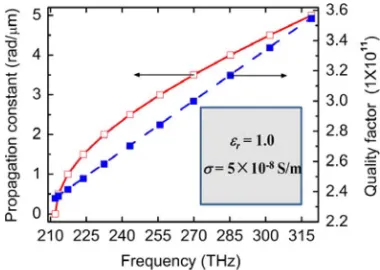
Fig. 1. Propagation constant and quality factor of the fundamental mode versus mode frequency in a metallic waveguide as shown in the inset, calculated by the compact 2-D FDTD method and the PAT technique (dots) and by the analytical formula (line).
We can build the DFT into the FDTD solver, so that we can per-form the DFT while updating the FDTD iterations. For the mode with the frequency , the DFT is defined as [16]
(8)
where is the number of time steps, is the mesh point in the computational window, is the time step, and represents an electromagnetic field component.
III. MODELVALIDATION
Before using the approach to analyze leaky modes in real semiconductor waveguides (as in such cases the leaky loss could be quite low), first we demonstrate that the PAT technique can efficiently analyze very low level of modal losses. For this val-idation a perfect metal waveguide with the mode quality factor as high as is considered. The structure we simulated is a square waveguide with the side length of 1.0 m formed by perfect metals and filled with a slightly lossy medium
S/m), as shown in the inset of Fig. 1. The mode frequency and quality factor of the fundamental mode of this metal waveguide can be calculated analytically using the following formula:
(9)
good agreement with the theoretical values: 211.985 THz and .
IV. NUMERICALANALYSIS
The waveguides we analyze in the following have mirror symmetry with respect to the waveguide axis, so the symmetry or anti-symmetry conditions can be added to the electric field components at the symmetry plane to excite the even and odd modes, respectively, which will save the computation domain by half and thus save the computation time greatly. The Gaussian function modulated cosine impulse is added to the field at several arbitrary points inside the waveguide core as the exciting source along with the proper propagation constant . The excitation is added to the component which is the major electric field. We avoid those high symmetry points in our selection because at these positions the specific mode field could be zero. Several modes can be excited simultane-ously. The time variations of the field component at several selected points different from those excitation points inside the waveguide core are recorded as the FDTD output. Then we calculate the field spectrum from the FDTD output by the Padé approximation transform. We can use any field component and get same results for the calculation.
Using the compact 2-D FDTD we can calculate the mode in-formation at a given propagation constant , which means the analyzed mode is operated at the wavelength . To analyze the mode at a specific wavelength , the proper propagation con-stant should be predicted and selected to excite this mode. Generally, we first calculate the effective index of the wave-guide mode through the effective index method (EIM) and get a propagation constant at the wavelength . We run the FDTD solver at this and calculate the mode wavelength by the PAT technique. Next we change the wavelength and get the new propagation constant by the EIM method, with which we run the simulation again and calculate the new mode wavelength. After several simulations a - dispersion curve can be obtained, from which we can extract the proper propagation constant rela-tive to the wavelength .
After the proper propagation constant is extracted, we run the FDTD solver for a relatively long time at this specific propaga-tion constant and through the PAT technique we can calculate the mode information at the particular wavelength. In the PAT calculation the number (length) of time steps of the field com-ponent input to the PAT transform are increased from short to long and the result is recorded only when a converged value has been obtained. This is the fundamental requirement for the PAT transform to calculate any mode information. Since the mode loss is proportional to the 3-dB bandwidth of the mode spec-trum, the mode with a lower loss generally needs a higher reso-lution, which means a longer time sequence is needed to obtain an accurate result because the spectral resolution is generally inversely related to the length of the time sequence.
A. 3-D ARROW Leaky Waveguide
[image:4.594.348.506.63.219.2]The 3-D ARROW waveguide we considered first has the same structure as in [1] which is shown in Fig. 2. The refractive in-dexes are 3.590 for GaAs, 3.555 for 5% AlGaAs, and 3.452 for 20% AlGaAs, and the operating wavelength is 1.064 m. Taking the advantage of the waveguide symmetry, only half of the structure is simulated by employing a perfect electric wall
Fig. 2. Schematic structure of the cross section of the ARROW leaky waveguide.
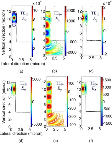
Fig. 3. (a) Calculated field intensity spectrum of the fundamental mode; (b)–(f) Contour plot of the dominant electric field distribution for
TE ; TE ; TE andTE modes calculated by the built-in DFT.
at the vertical symmetry plane to simulate the first 5 symmetric transverse electric (TE) modes ( and ). The UPMLs with 100-cell thickness are used to termi-nate the computation window with a uniform space cell size of 0.0125 m.
The field intensity spectrum of the fundamental mode cal-culated by the PAT technique from FDTD output sequences longer than 30 000 after the pulse finished is stable as shown in Fig. 3(a), which shows a very good Lorentzian line shape. The contour plots of the main electric field component for these five modes are also given by the built-in DFT as shown in Fig. 3(b)–(f) for the fundamental mode as well as the first four higher order symmetric TE modes. The calculated quality fac-tors for these first 5 symmetric TE modes at a wavelength of
[image:4.594.305.550.262.529.2]TABLE I
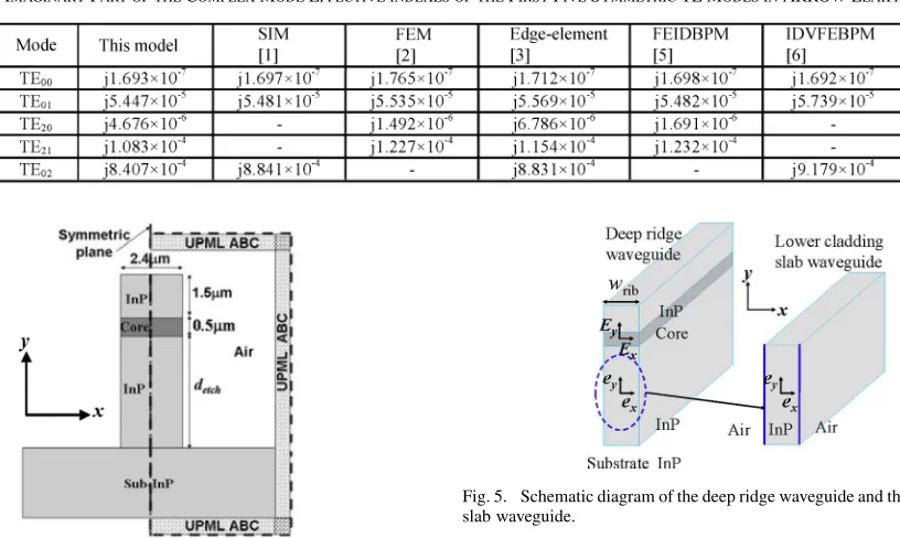
CALCULATEDIMAGINARYPART OF THECOMPLEXMODEEFFECTIVE INDEXES OF THEFIRSTFIVESYMMETRICTE MODES INARROW LEAKYWAVEGUIDE
Fig. 4. Schematic structure of the simulated deep ridge waveguide.
and , respectively, with the corresponding group in-dexes calculated as 3.600, 3.618, 3.647, 3.668, and 3.647. Then the corresponding imaginary part of the mode effective in-dexes can be calculated. Results are shown in Table I and com-pared with other methods in the references, which shows that the difference is within 12% between our results and those ob-tained by the other methods for four of the five modes in Table I, and for the mode, the calculated results is in qualitative agreement [10] with other methods which typically work in the frequency domain and most of them are finite-element-based.
B. 3-D Deeply Etched Ridge Waveguides
Then we analyze a 3-D deep ridge waveguide as shown in Fig. 4 with the same structure as in [7], [10] with the refrac-tive index of 3.2543 for the InGaAsP core with the thickness of 0.5 m at the wavelength of 1.55 m. Also only half of the struc-ture is considered by employing a perfect magnetic (electric) wall at the vertical symmetry plane to simulate the
mode. UPML ABCs with a 1 m thickness are applied on all the other outer boundaries with the distance of 3 m from the ridge to the PMLs for both the bottom and side boundary. A uniform space cell is used in the simulation with a size of 0.02 m. In [10] it is observed that instead of continuously dropping, the loss of the mode tends to saturate when the etching depth under the waveguide core goes beyond 2 m for a ridge width of 2.4 m. It is also found that the loss of both and modes tends to saturate when the etching depth is very deep for the ridge width narrower than 3 m [17]. The reason for this leaky loss saturation with a very deep etching depth is that the power carried by the minor electric field of these leaky modes in the ridge waveguide couples to the modes in the lower cladding slab waveguide, and loses energy downwards.
[image:5.594.93.501.85.329.2]1) Mode Coupling Effect: When the ridge is deeply etched, the lower cladding InP layer under the waveguide core forms
Fig. 5. Schematic diagram of the deep ridge waveguide and the lower cladding slab waveguide.
a slab waveguide confined by the air in the horizontal direc-tion as shown in Fig. 5. The lower cladding slab waveguide has its own te and tm modes. The tm mode has the major electric field component and the minor component, and te mode only has the component. The ridge waveguide has TE and TM modes but we focus on the TE mode here. The TE mode of the ridge waveguide has the major electric compo-nent and the minor electric component. For the mode cou-pling to efficiently happen, the mode symmetry-matching and phase-matching conditions have to be satisfied, which means the slab modes have the same symmetry properties along the horizontal direction with the ridge waveguide modes and have an effective index not less than those of the ridge waveguide modes. For the symmetry matching, the coupling may happen between the mode of the ridge waveguide and the funda-mental te mode or first order tm mode of the lower cladding slab waveguide; or between the mode and the first-order te mode or second-order tm mode of the lower cladding slab waveguide.
We use the effective index method (EIM) method to calculate the mode effective indexes of the ridge waveguide mode (for this deep ridge waveguide, the EIM method can generate modal effective indexes with high accuracy). By solving the three-layer slab waveguide in the horizontal direction, the mode effective indexes of the slab modes in the lower cladding slab waveguide can also be easily calculated. Fig. 6 shows the calculated modal effective indexes for the ridge width of 1–3 m, from which we observe that only the mode has an effective index larger than the mode. This means the coupling will only occur between the slab waveguide mode and the ridge waveguide mode, and there will be no coupling between the mode and the
Fig. 6. Mode effective indexes of leaky modes in very deeply etched ridge waveguide and slab modes in the lower cladding slab waveguide.
Fig. 7. Calculated field distribution ofE ; E ; E component of leaky modes in very deep ridge waveguide with a ridge width of 2.4m for theTE mode from (a) to (c) and theTE mode from (d) to (f).
coupling for the and components). This coupling results in the leaky loss saturation behavior for the leaky modes when the etching depth under the waveguide core is very deep.
Fig. 7 shows the field component distributions obtained from the built-in DFT from 80 000 FDTD iterations for the and modes in the deep ridge waveguide with an etching depth under the core of 6 m and a ridge width of 2.4 m. It can be observed that the and components in the lower cladding slab waveguide are not excited, while the component is ex-cited strongly. This confirms the above analysis.
When the coupling effects occur, the propagation constant of slab waveguide mode can provide a component matching to the propagation constant of the ridge waveguide mode and simulta-neously provide another component pointing downward which carries energy away from the ridge waveguide. From the field distribution of the component shown in Fig. 7(b) and (e), the
Fig. 8. Field distribution ofE along the vertical direction (horizontally at peak) for (a)TE and (b)TE mode in the deep ridge waveguide with an etching depth of 6m and a ridge width of 2.4m.
mode demonstrates propagation behavior in the lower cladding slab waveguide. For 2.4 m ridge width, the mode effective in-dexes of the and mode at 1550 nm are calculated to be 3.1393 and 3.0488, respectively, and are 3.1536 and 3.1098 for the and mode in the lower cladding slab waveguide, respectively. Therefore, according to the above explanation, the mode field should propagate in the lower cladding slab wave-guide downwards with a propagation constant as
(10)
which is 1.50 and 2.49 rad/ m for the and mode, respectively. We plot the distribution of the component along the vertical direction (horizontally it is at peak) in Fig. 8(a) and (b) for the and mode, respectively. The peak-peak single period length in the vertical direction is around 4.26 and 2.55 m for the and mode, respectively, from the figure, which results in propagation constants around 1.47 and 2.46 rad/ m which agree well with the above values. This confirms further that the modes excited in the lower cladding slab waveguide through mode coupling are the and
mode, respectively.
[image:6.594.52.275.232.519.2]Fig. 9. Calculated propagation loss of leaky modes in a deep-ridge waveguide versus ridge width with the etching depth under the core as 1, 2 and 6m for (a)TE and (b)TE mode.
of both the and mode decreases with the ridge width increase for the three etching depths under the waveguide core. This is because the narrow ridge waveguide has a smaller mode effective index as shown in Fig. 6. From the above analysis when the ridge is really deeply etched, a lower cladding slab waveguide is subsequently formed and supports slab modes. The higher order leaky ridge mode will couple to the slab mode and loses energy downwards once the slab mode satisfies both phase-matching and horizontal symmetry-matching to the ridge waveguide mode. As shown in Fig. 6, the narrow ridge wave-guide has a bigger difference of the effective refractive indexes
between the coupled mode and mode,
[image:7.594.337.517.66.208.2]the leaky energy will be larger than that of the wide ridge wave-guide. However, from Fig. 9(a) and (b) it is also observed that at specific ridge width, the leaky loss nearly disappears. For the waveguide with etching depth under the core near 1 m, the can-cellation phenomena are very weak, while they become signif-icant with the etching depth increases at the same ridge width. When the etching depth reaches 6 m, the cancellation peaks become very sharp and in this case the leaky loss is very low, generally several order of magnitude lower than normal values, and the leakage at the narrow ridge width is larger than that at the wide ones. In the simulated ridge width range, the cancel-lation ridge widths are around 1.2 and 1.84 m for the mode, and 1.12, 1.6 and 2.44 m for the mode. This can-cellation effect is due to the fact that the coupled slab mode in the lower cladding slab waveguide interferes destructively at specific ridge widths, which prevents energy leaking to the substrate.
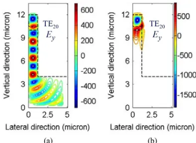
Fig. 10. Contour plot of the field distribution of theE component ofTE mode at ridge width of: (a) 2.12m and (b) 1.84m.
Fig. 11. Contour plot of the field distribution of theE component ofTE mode at ridge width of: (a) 2.12m and (b) 2.44m.
To understand the above leakage cancellation behavior, we analyze the mode field distributions of these two modes for very deep etching depths up to 6 m. Fig. 10 shows the com-ponent distribution of the leaky modes at the cancellation and normal ridge width calculated from the embedded DFT. It can be obviously seen from Fig. 10(a) that the coupled slab mode shows strong propagation in the lower cladding slab waveguide and the energy strongly leaks to the substrate for the mode at ridge width of 2.12 m, while from Fig. 10(b) the field in the slab and substrate is much weaker which means no significant coupling occurs at the cancellation ridge width of 1.84 m. For the mode given in Fig. 11, at the ridge width of 2.12 m the field in the slab is strongly leaky through the slab while at the cancellation ridge width of 2.44 m the field in the slab is much weaker in (a) and (b), respectively.
[image:7.594.328.525.251.395.2]V. CONCLUSION
The compact 2-D FDTD method with UPML boundary con-dition combined with the PAT technique has been introduced for leaky modes analysis. Compared with the frequency domain mode solvers based on the complex root searching, this model is easy to implement and can calculate the mode loss and the propagation constant separately and reliably. As a time-domain method it takes into account all mode coupling effects natu-rally in the simulation, which makes it very suitable to analyze leaky modes with a very low level of leakage. To validate the efficiency of this model, a perfect metal waveguide and a 3-D ARROW waveguide are analyzed. The approach is also used to analyze a 3-D deep ridge waveguide and leakage cancellation behavior for high order leaky modes in very deeply etched ridge waveguides at specific ridge widths has been observed.
REFERENCES
[1] G. M. Berry, S. V. Burke, J. M. Heaton, and D. R. Wight, “Analysis of multilayer semiconductor rib waveguides with high refractive index substrates,”Electron. Lett., vol. 29, pp. 1941–1942, 1993.
[2] H. E. Hernández-Figueroa, F. A. Fernández, Y. Lu, and J. B. Davies, “Vectorial finite element modeling of 2-D leaky waveguides,”IEEE Trans. Magnet., vol. 31, pp. 1710–1713, 1995.
[3] S. Selleri, L. Vincetti, A. Cucinotta, and M. Zoboli, “Complex FEM modal solver of optical waveguides with PML boundary conditions,”
Opt. Quantum Electron., vol. 33, pp. 359–371, 2001.
[4] W. P. Huang, C. L. Xu, W. Lui, and K. Yokoyama, “The perfectly matched layer boundary condition for modal analysis of optical waveg-uides: leaky mode calculations,”IEEE Photon. Technol. Lett., vol. 8, pp. 652–654, 1996.
[5] Y. Tsuji and M. Koshiba, “Guided-mode and leaky-mode analysis by imaginary distance beam propagation method based on finite element scheme,”J. Lightw. Technol., vol. 18, pp. 618–623, 2000.
[6] S. S. A. Obayya, B. M. A. Rahman, K. T. V. Grattan, and H. A. El-Mikati, “Full vectorial finite-element-based imaginary distance beam propagation solution of complex modes in optical waveguides,”
J. Lightw. Technol., vol. 20, pp. 1054–1060, 2002.
[7] M. Kohtoku, T. Hirono, S. Oku, Y. Kadota, Y. Shibata, and Y. Yoshikuni, “Control of higher order leaky modes in deep-ridge waveg-uides and application to low-crosstalk arrayed waveguide gratings,”J. Lightw. Technol., vol. 22, pp. 499–508, 2004.
[8] S. Xiao, R. Vahldieck, and H. Jin, “Full-wave analysis of guided wave structures using a novel 2-D FDTD,”IEEE Microw. Guided Wave Lett., vol. 2, pp. 165–167, 1992.
[9] S. Xiao and R. Vahldieck, “An efficient 2-D FDTD algorithm using real variables,”IEEE Microw. Guided Wave Lett., vol. 3, pp. 127–129, 1993.
[10] Q. Lu, W. Guo, D. Bryne, and J. Donegan, “Analysis of leaky modes in deep-ridge waveguides using the compact 2-D FDTD method,” Elec-tron. Lett., vol. 45, pp. 700–701, 2009.
[11] J.-P. Berenger, “A perfectly matched layer for the absorption of elec-tromagnetic waves,”J. Computational Phys., vol. 114, pp. 185–200, 1994.
[12] S. D. Gedney, “An anisotropic perfectly matched layer absorbing medium for the truncation of FDTD lattices,”IEEE Trans. Antennas Propag., vol. 44, no. 12, pp. 1630–1639, Dec. 1996.
[13] W. Guo, W. Li, and Y. Huang, “Computation of resonant frequencies and quality factors of cavities by FDTD technique and padé approxi-mation,”IEEE Microw. Wireless Compon. Lett., vol. 11, pp. 223–225, 2001.
[14] A. C. Cangellaris, “Numerical stability and numerical dispersion of a compact 2-D/FDTD method used for the dispersion analysis of waveg-uides,”IEEE Microwave Guided Wave Lett., vol. 3, no. 1, pp. 3–5, Jan. 1993.
[15] W. Kuang, W. J. Kim, A. Mock, and J. O’Brien, “Propagation loss of line-defect photonic crystal slab waveguides,”IEEE J. Sel. Top. Quantum Electron., vol. 12, no. 6, pp. 1183–1195, Nov./Dec. 2006. [16] M. Tong and Y. Chen, “Analysis of propagation characteristics and
field images for printed transmission lines on anisotropic substrates using a 2-D FDTD method,”IEEE Trans. Microw. Theory Tech., vol. 46, pp. 1507–1510, 1998.
[17] Q. Lu, W. Guo, D. Bryne, and J. Donegan, “Analysis of leaky modes in very deeply etched semiconductor ridge waveguides,”IEEE Photon. Technol. Lett., accepted for publication.
[18] M. A. Webster, R. M. Pafchek, A. Mitchell, and T. L. Koch, “Width dependence of inherent TM-mode lateral leakage loss in silicon-on-insulator ridge waveguides,”IEEE Photon. Technol. Lett., vol. 19, no. 6, pp. 429–431, Mar. 2007.
[19] T. Nguyen, R. Sekhar, M. Webster, T. Koch, and A. Mitchell, “Analysis of lateral leakage loss in silicon-on-sinsulator thin-rib waveguides,” inProc. Opto-Electron. Commun. Conf./Australian Conf. Opt. Fiber Technol., 2008, pp. 1–2.
[20] K. Ogusu, “Optical strip waveguide: A detailed analysis including leaky modes,”J. Opt. Soc. Amer., vol. 73, no. 3, pp. 353–357, 1983. [21] S. T. Peng and A. A. Oliner, “Leakage and resonance effects on strip
waveguides for integrated optics,”Trans. Inst. Electron. Jpn., vol. E61, pp. 151–154, 1978.
Qiaoyin Luwas born in Jiangsu Province, China, in 1974. She received the B.Sc. and M.Sc. degrees in optics from the Changchun Institute of Optics and Fine Mechanics, Changchun, China, in 1998 and 2001, respectively, and the Ph.D. degree from the Institute of Semiconductors, Chinese Academy of Sci-ences, Beijing, China, in 2004, studying the FDTD simulation and fabrication of photonic microcavities.
She is currently a Postdoctoral Researcher with the School of Physics, Trinity College, Dublin, Ireland. Her current research is focused on designing single-mode lasers and high-speed photodetectors.
Weihua Guowas born in Hubei province, China, in 1976. He received the B.Sc. degree in physics from Nanjing University, Nanjing, China, in 1998, and the Ph.D. degree from the Institute of Semiconductors, Chinese Academy of Sci-ences, Beijing, China, in 2004. His Ph.D. research was on FDTD simulation and fabrication of optical microcavities and design of semiconductor optical amplifiers.
Since September 2004, he has been a Postdoctoral Researcher with the De-partment of Physics, Trinity College, Dublin, Ireland. His current research is focused on optimizing microcavity two-photon absorption photodetectors and designing tunable integrated sources for coherent WDM systems.
Diarmuid C. Byrnewas born in Donegal, Ireland, in 1983. He received the B.A. (mod) and Ph.D. degrees from the School of Physics, Trinity College, Dublin, Ireland, in 2005 and 2009, respectively.
His current research interests include design, characterization, and applica-tions of widely tunable semiconductor lasers.
John F. Donegan(M’04–SM’08) received the B.Sc. and Ph.D. degrees in physics from National University of Ireland, Galway, Ireland.
He held postdoctoral positions with Lehigh University, Bethlehem, PA, and the Max Planck Institute, Stuttgart, Germany. He is a Professor of physics with Trinity College, Dublin, Ireland. His research interests are in photonic structures including broadly tunable lasers based on etched slots, microcavity two-photon absorption detectors, spherical microcavity structures, and photonic molecules. He also studies the interaction of quantum dots with human macrophage cells.