Hardware Manual
Peter A. Stark
Copyright © 1987 - 1991 by Peter A. Stark
and licensed to
Star-K Software Systems Corp. P. O. Box 209
Mt. Kisco, NY 10549 (914) 241-0287
All Star-K computer materials are licensed on an "as is" basis without warranty. Star-K Software Systems Corp. shall have no liability or respon-sibility to customer or any other person or entity with respect to any liability, loss or damage caused or alleged to be caused directly or indirectly by computer equipment or materials sold by Star-K, including but not limited to any interruption of service, loss of business or anticipatory profits or consequential damages resulting from the use or operation of such computer or computer programs.
Wherever used in this manual, HUMBUG® and SK*DOS® are regis-tered trademarks of Star-K Software Systems Corp. This is revision 1.01 of the manual, last revised on March 8, 1991
0. Introduction 1
1. Overview of a Micro Computer 3
2. The Power Supply 13
3. LED Indicators 21
4. The RESET Circuit 27
5. Master Clock Circuit 31
6. 68000 Operation 35
7. 68000 Operation in an Open Loop 47
8. The MAP Circuit 53
9. The Bus Error Circuit 59
10. The Address Decoder 63
11. The DTACK Circuit 71
12. ROM and Static RAM 75
13. The Magic Moment: First Signs of Life 79
14. Serial Interface 87
15. PC-Compatible Keyboard 93
16. PC-Compatible Bus Connectors 97
17. Computer Memories 105
18. DRAM Circuitry 113
19. Floppy Disk Controller 127
20. Parallel Printer Port 135
21. Optional -HDO Hard Disk Port 139
22. Loose Ends 143
APPENDICES
A. SK68K Parts List 145
B. Computer Number Systems 149
C. How to Solder 171
D. Disk Organization 175
Chapter 0
Introduction
The microprocessor has brought about a revolution in computing. Whereas twenty or thirty years ago, computers were so expensive that only large organizations could afford them, the microprocessor has brought computers not just into the small company, but also into the home, the small office, and even into industrial and consumer equipment.
At this time, microprocessors are broken down into two major catego-ries: CISC and RISC.
CISC microprocessors are Complex Instruction Set Computers. These are the traditional processors, which can execute a relatively large number of fairly complex instructions. RISC processors, on the other hand, are Reduced
Instruction Set Computers, which can perform a smaller number of relatively
simpler instructions. Right now, there is some disagreement about which are better. RISC processors, because they do less in each instruction, can be built so they do it faster. But this is outweighed to some extent by the fact that a larger number of instructions is needed to finish a particular job, and so it is not quite so clearcut which is faster on complex jobs.
In the CISC world, there are two major companies building micropro-cessors: Intel and Motorola. Intel was the very first microprocessor manu-facturer, and Motorola was the second, and they have been the two major players ever since. Both make very capable products, and are forever playing leapfrog, trying to best each other. At any given time, one or the other may be out in front.
68000 - they tried to keep the “flavor" of their earlier machines, but they did not keep any of their limitations. Thus many users agree that the Motorola 68000 is easier to use - and certainly more pleasant to use - than the comparable Intel processors.
When higher level languages are used, it doesn’t much matter to the programmer which processor they will eventually run on. But to get the utmost speed or compactness out of a program requires assembly language, and that is where programmers most often choose Motorola processors, which are much more orderly in their structure and easier to program on that level.
This book is about the 68000 Microprocessor and how it is used. We will cover many details of both its internal operation, the external circuitry it connects to, and the programs which it runs. Although Motorola makes more advanced 68000-family processors (such as the 68020 and 68030), almost all of the principles you will learn about the 68000 apply to those as well - they are merely extensions of the basic 68000 architecture.
When you look at the heavy-duty number-crunching applications of microprocessors, you will find the Motorola 68000 family used more often than any other. Even though the 68000 may be one of the slower micropro-cessors in the series, it is no slouch.
The 68000 is the microprocessor that gives the Atari ST, Commodore Amiga, and the Macintosh SE their power. It is also found inside many laser printers, as well as in industrial controllers and scientific workstations. The 68000 is roughly in the middle of what many call the ’68K’ family of processors - the 68008 is slightly below, the 68020 and 68030 are above. (A fifth processor, the 68010, is theoretically faster than the 68000, but the 68000 can be run at faster clock rates and so is just about equal in practical speed.) Our method for teaching you about the 68000 is to have you build and use an actual system.
In Volume I, you will concentrate on hardware. You will start from the very beginning, mounting one part after another, until you have a complete system up and running. As we go, we will discuss each part of the system, see where it fits into the overall picture, build it, and then test it.
Chapter 1
Overview Of A Micro Computer
The typical computer consists of the following parts:
1. The Central Processing Unit or CPU, which does the actual processing, arithmetic, and decision-making of the computer, and also controls the operation of the rest of the computer.
2. The memory, which stores programs being performed, as well as data and results.
3. Input and output equipment (also called I/O devices), which includes things like printers, keyboards, and the like. Furthermore, there are circuits called I/O interfaces which connect the I/O devices to the CPU and memory. (This definition leaves the status of things like disk drives and tape drives a bit hazy - some people would include these in the memory category, and some in the I/O category. We will use the latter.)
With this breakdown in mind, we can look at the types of computers. Historically, as well as in size order, computers can be broken down into four types:
a. Mainframe computers are the very large ones, which often occupy an entire room (perhaps even a very large room). Originally, of course, all computers were this large; these days, computers like these are used by the Internal Revenue Service, large corporations, or universities for commercial or research applications. In a typical mainframe computer, the CPU might be in one floor-standing cabinet, the memory in another, I/O interfaces in another, and the actual I/O devices in a few more. b. Minicomputers are smaller and newer, usually occupying one or more
large mainframes. In a typical minicomputer, The CPU might be one or more printed circuit boards, the memory might be a few more, and each I/O interface might be one or more pc boards as well. But all of these might be mounted in the same cabinet.
c. Micro computers are generally quite small, usually in desk-top cabinets, and less powerful than either of the above. But, given enough memory, these too can be used for both business and research applications. In most cases, the CPU is just one or two integrated circuits (ICs) occupying just part of a printed circuit board, which might even contain some memory or other circuitry as well.
d. Microcomputers (notice that we are now spelling it as one word, not two) are the smallest of the lot. In a typical microcomputer, a single integrated circuit contains the CPU, some memory, and even some of the I/O interfaces as well. In fact, the entire IC might be called a microcomputer. They are almost used strictly for control applications - for example, you might find one inside a camera or inside a traffic light.
The 68000 Microprocessor (also called a Micro Processing Unit, or MPU) would be the CPU in a Micro Computer. Actually, some of the 68000’s faster cousins are powerful enough that they can do jobs often reserved for minicomputers in the past. And so the distinction between the minicom-puter and the micro comminicom-puter is becoming blurred as time goes on. In fact, some people believe that the minicomputer may even cease to exist, as micro computers take over many of their jobs.
The SK68K Computer Trainer
As shown in the photograph of Fig. 1-1, the SK68K microcomputer trainer is all contained on one printed circuit board. It contains the follow-ing:
a. The 68000 microprocessor is the large integrated circuit near the bottom. b. The main memory consists of the 32 small integrated circuits in the bottom left corner plus the four medium size IC’s near the center. The 32 ICs in the corner provide 1 megabyte of dynamic RAM (the main random-access memory); the four IC’s in the center provide 4K (4 kilobytes) of static RAM with battery back up (the two slightly smaller ICs), and 32K of ROM (read-only-memory) with space for more (in the two slightly larger ICs).
d. Finally, the rest of the board contains various smaller ICs used for timing and control, and to interconnect the remaining parts together. In fact, these remaining ICs are often called glue chips for that reason.
The fact that the SK68K has connectors to accept XT-compatible clone components such as keyboards, video boards, and hard disk controllers, makes the SK68K somewhat unique. It allows us to expand the Trainer and give it additional capabilities, and do so at a very low cost by taking advantage of the fact that such clone components are produced in very large quantities and are therefore very inexpensive.
The Block Diagram
The best way to get an overall view of the SK68K trainer and how it works is to start with the block diagram in Fig. 1-2. In general terms, this diagram describes any microcomputer, not just the SK68K.
The heart of the diagram is the microprocessor, a Motorola 68000 in our case. It is driven by a clock, which is nothing more than a high frequency oscillator which generates a square wave. In the SK68K, this clock will most likely be an 8 MHz signal, though it could go as high as 16 MHz. The clock synchronizes everything occurring in the system so that it occurs at a fixed speed.
The right side of the diagram contains three essential parts: ROM, RAM, and I/O interfaces. ROM and RAM are both part of the computer’s mem-ory, but ROM can only be read (hence, its name read-only-memory or ROM), meaning that the data and programs in the ROM were placed there once the factory and can now be used by the trainer but not changed. RAM, on the other hand, is read-write- memory (somewhat misnamed as RAM rather than RWM - but then, have you ever tried to pronounce RWM?) The Trainer can write (store) data or programs in RAM, can later read them back, and can also change them at any time. Furthermore, ROM is permanent even when the power is turned off, whereas RAM is erased when power disappears (unless special precautions are taken, such as providing a small battery to keep the RAM powered up even when the rest of the system is shut off. Such memory is called battery backed-up.)
The ROM
The ROM in the SK68K system consists of two 28-pin ICs called EPROMs or Erasable Programmable ROMs. If you purchased these from an electronic distributor, they would be empty or erased. But the two EPROMs which come with the SK68K kit have been programmed with a copy of the HUMBUG debugging program and with a Basic translator. The
computer can read and use these programs, but cannot erase or change them.
The RAM
The SK68K computer’s RAM consists of two parts - static RAM, and dynamic RAM.
Most computers would generally have either static RAM (abbreviated SRAM) or dynamic RAM (DRAM), but not both. We use both because they each have their advantages and disadvantages. For large memories, dy-namic RAM is cheaper and smaller - without it, it would not be practical to provide 1 megabyte of static RAM at a reasonable cost. On the other hand, for small memories static RAM is the right choice because it is much simpler - and easier to debug in case of problems! Hence the SK68K computer will first be built with a small amount of static RAM using just two integrated circuits. Since the static RAM circuitry is so simple, it will probably work immediately without any problems, giving us the ability to run Basic and HUMBUG. Once the static RAM is all working, then we can add the dynamic RAM, consisting of thirty-two 256K dynamic RAM ICs plus a batch of support ICs. If there is a problem, we can use HUMBUG to debug the dynamic RAM. This kind of bootstrapping makes the building of a large system like the SK68K from scratch a lot more practical.
There is actually an ulterior motive to providing static RAM - to provide a clock/calendar we need only unplug one of the RAM ICs and substitute a clock/calendar IC which is totally pin compatible. We will use the MK48T02 which provides not only a clock and calendar, but also some static RAM of its own - and a built-in battery to keep the clock and RAM going while the computer is turned off.
I/O Interfaces
Although Fig. 1-2. shows just a single box labelled I/O Interfaces, the SK68K computer’s I/O is actually quite complex. It consists of two MC68681 DUARTs to provide four serial interfaces, one 68230 parallel interface/timer, a 1772 floppy disk controller, keyboard interface, speaker interface, a number of extra support ICs, all of the circuitry needed to interface to the six PC-compatible interface connectors, plus the interrupt circuitry shown at the bottom, which allows I/O devices to interrupt the 68000 when they need it; the latter is absolutely essential for using a clone keyboard.
Some microcomputers often also provide DMA or Direct Memory Ac-cess circuits. This is a feature which is often used when the CPU has difficulty keeping up with fast I/O devices such as disk drives. Since the 68000 does not have any problems keeping up (and DMA really complicates the computer), we chose not to use it in the SK68K computer.
The Data Bus
address bus. The term bus is used to signify that a number of parallel wires are used to carry data simultaneously.
The data bus is used to move numbers (which could be numeric data, instructions, or text) between the microprocessor, memory, and I/O de-vices. If you look at the arrowheads at the ends of the data bus in Fig. 1-2, you will see why the data bus is said to be bidirectional. Data may go in either direction - left or right.
In our case, the data bus consists of 16 wires, each of which carries one bit or binary digit. (See Appendix B if you are not that familiar with binary numbers and bits.) Thus the 68000 can transfer a 16-bit number to or from the microprocessor all at once. As we will see, however, the 68000 handles numbers in chunks of 8 bits (called a byte), 16 bits (two bytes, also called a word), or 32 bits (four bytes, also called a long word.) When transferring a byte, the 68000 uses only half of the data bus; when transferring a long word, it uses the data bus twice, transferring 16 bits at a time.
The number of bits on a data bus also called the width of the bus -obviously has a bearing on the speed - the wider the bus, the more bits can be moved at a time, so the faster the computer runs. But there is more to the story - the size of numbers that can be handled internally in the micropro-cessor is also important.
The very first general-purpose microprocessors - the 8080, 6800, 6502, and Z-80 - had an 8-bit data bus and also handled 8-bit numbers internally. For this reason these were called 8-bit microprocessors.
The next generation of chips, such as the 6809 and 8088, still had 8-bit data buses, but could now handle 16-bits internally. This gave them extra power, but they were still bogged down by the slow speed at which they could transfer data to and from memory and I/O devices.
The next step up included the 8086, 80186, and 80286, processors which could handle 16-bit numbers both internally and externally, and which are called 16-bit processors.
The 68000 is one step higher yet - it still only has a 16-bit data bus, but can handle 32-bit numbers internally.
Finally, at the top of the current pyramid are the 80386 and 68020, both of which handle 32-bit numbers both internally and on the data bus. These are true 32-bit processors.
from memory. The 68000 does have a small cache, but it is too small to provide a significant saving.
The Address Bus
The other major bus, the address bus, carries addresses. That is, in order to save data into memory, or read data from memory, the processor must specify exactly where in memory that data is located. This is done with a numeric address, sent out on the address bus. As you can see from the arrowheads in Fig. 1-2, the address bus carries data from left to right; that is, it is unidirectional. (There is an important exception - when a computer uses DMA, then addresses may come out of an I/O interface and travel to the left.)
The width of the address bus determines exactly how much memory a computer can have. If the bus had only three lines, for example, then each address would consist of just three bits. Since each bit can only be either a 0 or 1, there would be just eight possible addresses - 000, 001, 010, 011, 100, 101, 110, or 111 - since there is no other three-bit number that can be made out of ones and zeroes. Hence the maximum number of addresses - or put another way, the maximum possible number of locations in the memory of this computer - would be eight, which also happens to be equal to two to the third power. That is, 23= 8.
In general, the maximum number of addresses is 2 to the same power as the number of address lines. For example, most 8-bit computers have 16 address lines in their address bus, so they have a maximum of 216= 65536 addresses.
Since a K in computer terms is 1024 (not 1000 as in ordinary electronics), 65536 works out to be exactly 64K locations.
Newer microprocessors have more address lines than their predeces-sors:
microprocessor address bus width (bits)
maximum memory size
8080, 6800, etc. 16 64K
8088, 68008, etc. 20 1 megabyte
68000 24 16 megabytes
68020, 80386 32 4 billion bytes
As you might expect, there is more to the story than just the width of the address bus. Consider the 20-bit bus of the 8088 and 68008, for example. Both of these processors can address up to a megabyte of memory, but the 68008 (the smaller cousin of the 68000) can do so in one continuous piece, whereas the 8088 must split that memory into 64K segments. Handling the segmenting greatly complicates a program - that’s why many programs written for the 8088 (such as Microsoft’s BASIC or BASICA) can only use 64K of memory at a time, whereas a Basic on the 68008 has no such limitation.
way that Intel and Motorola processors handle I/O. In a computer using a Motorola processor like the 6800 or 68000, the I/O interface connects to the processor in exactly the same way as the memory, with the result that memory and I/O use the same addressing scheme. Thus if the 68000 were to use 1 megabyte to address I/O, then there would only be 15 megabytes left for memory. Intel processors do not have that limitation - they use the entire normal address range for memory, and have a separate set of ad-dresses (usually much smaller) just for I/O. Although some people point this out as a weakness in the Motorola approach, in practice it makes very little difference since I/O seldom requires more than just a few dozen (or perhaps a few hundred) addresses. There are still plenty of addresses left for memory. In most cases, a 68000 or 68020 has so many possible addresses that we can afford to waste thousands - maybe even millions - of addresses on I/O without feeling the pinch.
[image:13.684.233.561.369.591.2]A list of addresses in a computer and what they are used for is called a memory map. Table 1-1 shows a simplified memory map of the SK68K computer. 1 As you can see, there is still plenty of memory left for expan-sion, probably a lot more than most of us would care to pay for.
Table 1-1. Simplified SK68K Computer memory Map
Memory Range (hex) Description
000000 - 0FFFFF Dynamic RAM (1 megabyte) 100000 - BFFFFF Empty - for expansion (11 megabytes) C00000 - DFFFFF Addresses for PC expansion slots (2
megabytes) E00000 - F7FFFF Unused (1.5 megabytes)
F80000 - F9FFFF ROM (128K)
FA0000 - FBFFFF Addresses for PC expansion slots (128K)
FC0000 - FDFFFF Unused (128K)
FE0000 - FE3FFF I/O Interfaces (16K)
FE4000 - FEFFFF Unused (48K)
FF0000 - FF7FFF Static RAM (32K)
FF8000 - FFFFFF Unused (32K)
The Address Decoder
As Fig. 1-2 shows, the address bus coming out of the microprocessor is split into two parts - part goes into the address decoder, while part goes to the ROM, RAM, and I/O interfaces.
The job of the address decoder is to look at the address on the bus and decide whom it’s intended for. For example, as Table 1-1 shows, the
namic RAM occupies addresses 000000 through 0FFFFF. Whenever the address decoder sees any address beginning with the hexadecimal digit 0, it recognizes it as a RAM address, and sends a signal to the RAM that effectively says “Hey, you! This address is meant for you ... go to work." This signal is called an enable or select signal. If it goes directly to an IC, then it is called a chip enable or chip select, often abbreviated CE or CS.
Fig. 1-2 shows just one address decoder, connected to the ROM, RAM, and I/O interfaces. In practice, though, most computers split that address decoder into two or more smaller decoders, each of which services just one part of the computer. Part of the reason is that it is easier to build that way, but there is a second reason as well - not all the decoders look at the same part of the address bus.
In the case of dynamic RAM, the address decoder need only look at the leftmost hex digit of the address; that is, it looks at the four leftmost bits, which must equal 0000 (a hex 0) for the RAM to go to work (see Appendix B for a discussion of binary and hexadecimal digits if you need to brush up.)
The decoder for the ROM, on the other hand, must look at seven bits. As Table 1-1 shows, the ROM occupies addresses F80000 through F9FFFF. Since there are other parts of the computer whose addresses also begin with the hexadecimal digit F, the ROM’s address decoder must look at more than just the first digit F - it must also check that the second digit is either an 8 or a 9. This is done by looking at individual bits of the address.
When written in binary, the lowest ROM address - F80000 - begins with the bits 1111100 and then continues with 17 zeroes, like this:
F80000 = 1111 1000 0000 0000 0000 0000.
The address F9FFFF also begins with 1111100 but then continues with 17 ones, like this:
F9FFFF = 1111 1001 1111 1111 1111 1111.
All other ROM addresses also begin with the bits 1111100, but have different combinations of 17 zeroes and ones at the end. Thus any address which starts with the bits 1111100 applies to the ROM; the ROM’s address decoder therefore looks for a 1111100 bit pattern in the first seven bits of the address, and sends an enable signal to the ROM as soon as it sees it.
Hence different parts of the address decoder look at different bits of the address bus. Some parts may only look at one or two bits, other parts may look at four or six, and some parts of a typical computer’s address decoder may look at 16, 32, or even more bits in some computers.
Conclusion
Chapter 2
The Power Supply
An unreliable power supply can play havoc with a computer. Yet the power supply is so common - and inconspicuous - that it is taken for granted and seldom suspected in case of a problem. Since nothing else can work without the power supply, let us start with it.
2-1. Discussion
The SK68K requires three power supply voltages. But it is difficult to say exactly how much current it needs at any specific time, since this depends on how far along you are in constructing it, and also on how many plug-in expansion boards are installed in the six XT-compatible connectors. A fully configured SK68K, with a full 1 megabyte of memory and all on-board options, requires the following:
+5 volts for the main TTL and MOS logic.
+12 volts for the RS-232C serial port, and for some of the I/O circuits. -12 volts for the RS-232C serial port, and for some of the I/O circuits. These voltages can be supplied from one or more regular power sup-plies, but the simplest and cheapest is a 135-watt or 150-watt switching power supply of the type designed for XT clones.
Types of Power Supplies
Switching power supplies are substantially smaller and more efficient than the old-fashioned “linear" power supplies. The block diagram of Fig. 2-1 shows the difference between the conventional linear supply and a switching supply.
then full-wave rectified, filtered, and then fed to a linear regulator. The most common regulator contains a pass transistor in series with the output, controlled by a voltage comparator which compares the DC output volt-age against a reference voltvolt-age. The comparator then biases the pass tran-sistor to change its resistance; it thus uses the voltage drop across the tran-sistor to keep the output DC voltage constant. If the output voltage is too low, it makes the pass transistor con-duct more; if the output voltage is too high, it biases the pass transistor so it conducts less.
There are three main problems with such a linear circuit:
(1) Since the AC line operates at 60 Hz, the step-down transformer must be fairly large and heavy. It must have enough iron in the core so as not to saturate at the low frequency.
(2) The filter capacitor must also be fairly large so as to remove the ripple, which occurs at twice the line frequency. Although the capacitor need not remove all the ripple (since the regulator can remove the rest), it must remove enough ripple to make sure the voltage fed to the regulator does not drop too far.
(3) The regulator’s pass transistor conducts current at all times, and there-fore dissipates power. To safeguard against the voltage dropping too far, the voltage level into the regulator must be at least several volts more than the desired output, so the power dissipated by the pass transistor may be considerable.
None of these problems is major, but it does mean that a linear power supply to provide a substantial amount of power must be fairly large and heavy, and must dissipate a substantial amount of power.
The switched-regulator supply of Fig. 2-1 (B) is substantially more complex. It starts with a rectifier and filter, which directly change the incoming 115 volts AC into DC at between 110 and 150 volts. This DC then powers an oscillator, which generates a high voltage AC at a frequency of several kHz. This signal is then stepped down through the transformer, rectified, and then filtered.
Regulation is achieved by again comparing the DC output of the supply against a reference voltage in a voltage comparator, and using the resulting output to control the pulse-width of the oscillator.
This circuit has several advantages over the linear supply:
(1) Since the transformer works at several kHz, rather than at 60 Hz, it requires a smaller iron core. A small toroid can be used with less loss and less cost.
needed in the input circuit, the oscillator will tolerate a large amount of ripple and thus a small capacitor can be used here as well.)
(3) Although the oscillator transistors indirectly provide regulation of the output, they do not operate in the linear region as the pass transistor would in a linear power supply. They are always either cut off or saturated, and so their power dissipation is much lower than in the linear region.
The result is that a switching power supply, although much more complex than a linear supply of the same output power rating, is generally much smaller and lighter, and runs much cooler. For example, a 135-watt or 150-watt power supply of the type often used in XT clones weighs only a fraction as much as an equivalent supply used to weight before switching power supplies became popular.
Needless to say, switching supplies do have some disadvantages. The major ones are this:
(1) Because the oscillator operates at fairly high powers and high frequen-cies, it can produce interference with nearby radio or television receiv-ers. The 115-volt input to the power supply must therefore be well filtered to prevent high frequency signals from being transmitted back into the power supply; additional filtering is also needed on the dc outputs as well, and the supply must be well shielded.
(2) Since the supply does not have a large output filter capacitor, it does not do well when the output current suddenly changes. In a conventional power supply, the output capacitor easily handles sudden surges in power; transient response of switching supplies tends to be slower. The lack of a large filter capacitor also means that switching power supplies are also much more susceptible to short power outages. For example, some users may use a UPS (Uninterruptible Power Supply) or standby power supply in case of main AC power failure. Such power supplies often delay a anywhere from 15 milliseconds to as much as 1/2 second after a main power failure before they switch in to provide power. The large filter capacitor in a linear power supply may be able to provide power to tide the computer over during this interval; in a switching power supply, there is no such storage capacitor and so the dc power may just totally disappear for this fraction of a second.
often hear it speed up or slow down slightly as the switching regulator changes its pulse width to keep the +5-volt output constant.
(4) Switching regulators do not work very well if there is no load. Most XT-type power supplies therefore have a protection circuit which turns off the entire power supply when the load is removed; the same circuit also turns off the supply if the dc output is shorted.
SK68K Power Supply Connector Pinouts
The XT-type power supply has six dc output connectors, two for the electronics and four for disk drives.
Two six-pin connectors plug into the main computer board (J10A and J10B in the right rear corner of the board). The only reliable way to differ-entiate between them is by the colors of the wires. In order, their 12 connections are as follows:
Pin number
Color Function
J10B
1 Orange Power Good (not used - see text)
2 - No Connection
3 Yellow +12 volts DC
4 Blue -12 volts DC
5 Black Ground
6 Black Ground
J10A
1 Black Ground
2 Black Ground
3 White -5 volts DC (not used)
4 Red +5 volts DC
5 Red +5 volts DC
6 Red +5 volts DC
These connectors provide two outputs which will not be used by our computer - a “power good" output which could have been used to detect that primary (115-volt) power has just disappeared and the dc outputs are also about to disappear, and a -5-volt output which is simply not needed. The remaining four power supply connectors are all wired identically as follows:
Pin number
Color Function
1 Yellow +12 volts DC
2 Black Ground
Pin number
Color Function
4 Red +5 volts DC
5-1/4" floppy and hard disk drives all use the same wiring, so such a power supply can directly power as many as four such drives (assuming that it has enough power handling capacity.) 3-1/2" drives use a different connector and pinout, and an adapter cable has to be used.
2-2. Construction
Before proceeding with actual work, it’s important to set things up so the SK68K printed circuit board can be worked on easily, yet is protected from accidental short circuits and other possible damage.
The best way to do so is to is to mount the board and its power supply on a wooden board about 12" by 24", as shown in Fig. 2-2. Hammer two brads into the board as shown to hold the printed circuit board in place. Be sure to use the correct two holes to avoid a possible short circuit. (The location of the two brads in Fig. 2-2 is shown with the small triangular flags
on the brads.)
Note how the board is ori-ented - power connector J10 is right next to the power supply, and the six expansion connec-tors are in the left rear corner. We will use the words left, right, front, and back to describe the board when it is positioned like this (it will fit into a PC clone cabinet the same way). For ex-ample, U92 is in the back, while C47 is in the front left corner. (Look at the silk-screen printing on the board to see how the com-ponents are positioned on the board.)
Note also that the side with all of the white lettering - this is called the silk-screen layer - is on top, whereas the other side of the board will be called the bottom. All of our soldering will be on the bottom side -there are no solder joints whatever on the top or silk-screen side of the printed circuit board.
Soldering itself is more of an art than a science. Even if you consider yourself to be an expert, read Appendix C for our hints on how to keep bad soldering from ruining your SK68K project.
The Power Connector
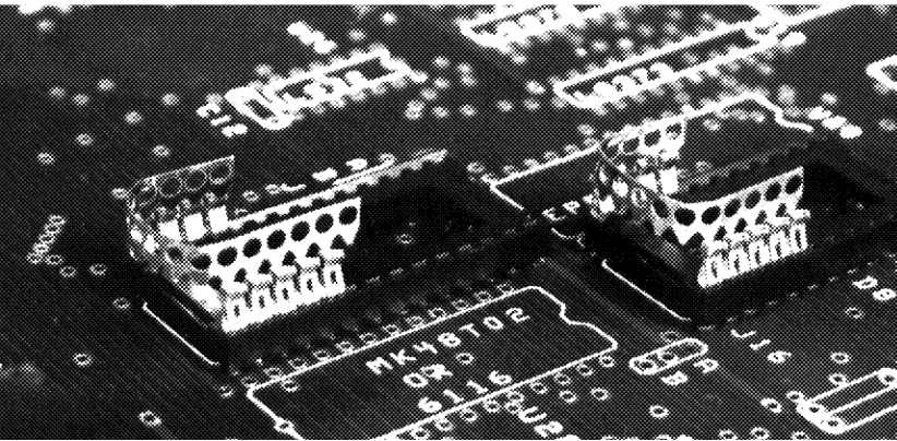
The power connector, J10, actually consists of two six-pin connectors, J10A and J10B, in the right rear corner of the board. They are shown in Fig. 2-3, J10A on the left and J10B on the right. Read the following paragraphs before you do anything.
The power connectors are a potential source of big problems. If you look at the connectors you have, you will note that the two board-mounted connectors are identical, and the two power supply plugs are probably identical as well. In other words, it is extremely easy to make a mistake and plug the wrong power supply plug into the wrong connector on the board and burn up the board. We have to make sure that never happens.
First, look at the two power supply plugs. You will see that one of them has six wires, while the other has only five - the next-to-the-last wire is missing. Note also that we have cut off the next-to-the-last pin on J10B in Fig. 2-3 (compare it with your connectors). Though this doesn’t really prevent a mixup, it does serve to remind us what goes where.
[image:21.684.153.531.154.408.2]the plugs and connectors are brand new, the tabs on the plugs prevent them from being inserted into the pc-mounted connectors because the long tabs hit the bridges. The object is to cut just the right combination of tabs and bridges so the six-wire plug only fits J10A, and the five-wire plug only fits J10B. If you look closely at Fig. 2-3, you will see that we have done exactly that. (The whole thing is complicated by the fact that the power supply plugs may already have some tabs cut off, so you may have to take that into account.)
One useful piece of information: when properly installed, the black wires of the two connectors are adjacent to each other.
Now that you know what has to be done, install the following compo-nents:
J10A and J10B Solder the two connectors to the board as in Fig. 2-3, and then match up the bridges and tabs so the power supply plugs in only one way. Make sure that the connectors are oriented the correct way, so that the metal pins are visible from the edge of the board, as in Fig. 2-3, and that the 5-wire plug only fits J10B. C65 10 µF tantalum capacitor; make sure that its positive
lead (marked by a + sign) is closer to J10, as tantalum capacitors have a nasty habit of exploding if connected backward!
C6 0.1 µF disk capacitor near J10 C3, C4, and C5 47 pF disc ceramic capacitors
C68 33 pF disc ceramic capacitor
Although not part of the power supply, the 47 pF and 33 pF capacitors are very similar to the many 0.1 µF capacitors, and this gets them out of the way so you will not confuse them later.
Aside from one 1 µF tantalum capacitor, all the remaining capacitors are 0.1 µF disc ceramics. Digital circuits are notoriously ’noisy’, and computer designers have learned the hard way that it is necessary to install small bypass capacitors between the +5-volt line and ground all over a board to keep that noise off the power lines. A general rule of thumb is that one such capacitor should be installed for every two or three digital ICs. We will instruct you when to install these additional capacitors.
2-3. Testing
Chapter 3
LED Indicators
First, a bit of theory and some terms we are going to need later. Even if you know all about logic circuits, read on - some of these concepts are a bit different in real life from the way they are sometimes written up in simple books and magazine articles.
3-1. Discussion
Digital circuits represent the binary digits 0 and 1 by means of voltages; in most microcomputers, the two voltages are often called low (which is a voltage between 0 volts and roughly 0.8 volt) and high (which is a voltage between about 2 volts and 5 volts). There are a few exceptions, of course -such as in an RS-232 circuit between a computer and terminal where larger positive and negative voltages may appear - but lows near 0 volts and highs near 3 to 5 volts are the most common. In any case, the range between 0.8 volts and 2 volts is a no man’s land; if a digital signal is in that range it usually indicates a problem somewhere.
Many people think that a low voltage is a 0, while a high voltage is a 1, but this is not always true - it could be the other way around. So talking about ones and zeroes can be ambiguous, while talking about lows and highs is always quite specific. Note that we don’t really care about the exact value of a signal’s voltage, so long as it falls into one of these two ranges.
But we can talk about digital signals in a different way as well - we can say that a particular signal is on, or off. Computer people, however, like somewhat longer words - they say that a signal is asserted when they really mean it is on, and they may say that it is negated when it is off.
A so-called active high circuit is one which is high when asserted (on), and low when negated (off); some books call this positive logic. A so-called active low circuit is one which is low when asserted (on), and high when negated (off); some books call this negative logic. In a typical computer, both kinds of circuits may be used, and often an active high circuit may be just a tenth of an inch from an active low circuit.
Many of the signals in this text and diagrams are assigned meaningful names. Whenever you see a name which has a “not bar" either above or below its name, such as HALT you will know that this signal is active low. On the other hand, a signal without the not bar, such as FC0 or A16, is active high. Because it is difficult to place not bars over signal names in text, many people use alternative ways of marking active low signals; some common ways are with an asterisk, as in HALT*, a minus sign, as in -HALT or HALT-, or with a lower case letter n, as in nHALT. We will use the not bar above the name in this book.
LED Indicators
[image:25.684.171.503.498.706.2]If, instead of using an XT-clone cabinet, you use what is commonly called a “mini-AT" cabinet (because it is the size of an XT cabinet, but is built in the style of an AT cabinet), you will note that such cabinets have two or three status indicator LEDs on the front panel. These LEDs can eventually connect to J15, J16, and J17 on the SK68K board as shown in Fig. 3-1 (which also shows the speaker wiring.) In each case, a resistor in series with the LED (or speaker) limits the current through it, while the LED (or speaker) is controlled by a section of U32, a 7406 open collector gate. (Note that U32c, U32f, U32d, and U32b are all part of the same U32 IC; U32 has six such inverters, and the other two are used elsewhere. The numbers on the
outside of the triangle, next to the leads, are the pin numbers. The vertical line inside the U32 symbol marks this as an open collector device, explained shortly. Ignore the fact that U32f has a small circle, called a bubble, on its input side instead of the output; this is just a different notation and will be explained next time shortly.
The LED at J15 lights whenever there is +5-volt power, while the LED at J17 lights when the 68000 is halted, and the LED at J16 lights to indicate hard disk use.
3-2. Construction
Since many users of the SK68K do not have access to an oscilloscope or even a logic probe, the wiring for the LED at J16 has been set up to allow its use as a simple logic probe. Furthermore, during construction you will not have the printed circuit board mounted in the cabinet, and so we want to connect LEDs directly to the board for immediate use. (This is especially important for the HALT LED, which will be very useful during checkout of the board.)
We therefore wire the circuit a bit differently. Refer to Fig. 3-2, the parts layout, and install the following parts:
R14, R15, and R16 330 ohm 1/4-watt resistors
R24 2200 ohm 1/4-watt resistor
C11 0.1 µF disk ceramic capacitor 14-pin socket for U32
R25 33 ohm 1/4-watt resistor
J18 4-pin header strip
Do not install U32 in its socket yet. (R25 and J18 are not needed yet, but this is a convenient time to install them as the speaker wiring is so similar to the LED wiring. But do not connect the speaker yet.)
Then install the three LEDs at J15, J16, and J17. The negative lead of each LED, usually marked by a small flat on the side, should go toward the resistors. If at all possible, check each LED first, since many times LEDs available on the open market are wired opposite to this convention.
Install each LED so it stands up straight, but the bottom of the LED is about 1/2" above the board. (The reason: When we’re ready to mount the board in the cabinet, we will cut off each LED lead just below the LED itself, and use the stubs of the LED leads as connectors for the panel-mounted LEDs.)
3-3. Testing
resistor between pins 7 and 14 of the U32 socket (don’t force the leads into the socket) and try again. This should add just enough of a load to allow the supply to turn on.
[image:27.684.169.529.152.634.2]If the LED does not light at all, even for an instant, then most likely either the LED is in backward, R14 is the wrong value, or the power supply is
defective or not properly connected to J10A and J10B. Correct the problem before continuing.
NOTE:
During construction, we will often wire something, turn on the power and try it out, turn off the power, wire some more, and so on. It is absolutely essential that you turn off the power before doing any wiring, soldering, or inserting ICs into sockets. Better yet, turn off the supply and also unplug it. If you slip and forget to turn off the power, you may well burn out part or all of the components on the board, and perhaps even burn out a few of the traces as well.
So now turn off the power, connect a thin wire about 12-15" long to terminal 1 of J14. Try to use a thin solid wire, about 30 gauge. If you use a stranded wire, then twist the strands of the loose end and cover them with a bit of solder so they stick together. Next, insert a 7406 IC into U32 (remove the 150- or 330-ohm temporary resistor). Note that all ICs on the entire board are oriented the same way - pin 1 (marked by a dimple or notch, both on the IC and also on the silk screen layer on the board) goes toward the back of the board. Then turn the power back on.
The wire connected to J14-1 (which is shorthand for terminal 1 of J14) is now a test probe, which we will call the LED probe. If you ground its loose end (to pin 7 of IC32, for example) then the LED at J16 should go off; if you connect it to a high voltage (pin 14 of IC32, for instance) then the LED should go on. The J16 LED now makes a simple logic probe which can be used to check out other parts of the computer. (If you have a meter, oscilloscope, or real logic probe, then feel free to use it instead, but you may still occasionally want to use this built-in probe instead.)
Chapter 4
The Reset Circuit
The 68000 microprocessor must be initialized when the system is first turned on, or whenever it must be restarted from a major error. This process is called resetting.
4-1. Discussion
Resetting is done by temporarily grounding two 68000 pins - the RESET line and the HALT line. Remember - the “not bar" denotes that these signals are active low. Hence grounding them, which forces them to a low, asserts these two lines or turns them on. Asserting RESET and HALT together for a minimum of 100 milliseconds resets the 68000 and gets it ready to run a program.
The 68000 should be automatically reset every time the power is turned on, but it is also useful to have a button which can be pushed to force a reset if the computer does something it is not supposed to do. Both of these functions are done with the circuit of Fig. 4-1.
its output (the LED circuit in Fig. 3-1 was a pullup in a way) it usually means somebody made a design error.
Whenever a pushbutton connected to J23 is pressed, this applies a low to pin 2, the trigger input of the timer, which causes the timer to ground pin 7, which discharges C63. (This also happens when power is first applied, since C63 would normally start off discharged). The 555 timer sees this low voltage on its pin 6, and therefore outputs a high on pin 3. This is inverted to a low by U22, and asserts a low on RESET and HALT of the 68000, resetting it. (The reset signal also goes elsewhere through U66e, but more on that later.)
As soon as the pushbutton is released (or the power supply voltage has risen), C63 starts to charge through R23. When it reaches about 3.3 volts, the 555 timer senses this rise and shuts off its output on pin 3; this removes the low from RESET and HALT, and lets the 68000 begin operating.
How long does it take for the voltage on C63 to reach 3.3 volts? About one time constant, which is defined as the product of R23 and C63. Since R23 is 1 megohm (1,000,000 ohms) and C63 is 1 µF (0.000001 farads), the product is 1,000,000 x 0.000001 = 1 second. Thus the RESET and HALT signals will go low for about 1 second at startup or whenever we push the reset pushbutton.
4-2. Construction
Install the parts listed below, but note that tantalum capacitor C63 is a polarized capacitor; its positive terminal must go toward pin 6 of U91. Also, the two-pin header strip for J23 has a short end and a long end; the short end goes through the board and is soldered on the bottom, while the long end sticks up.
R20 and R21 2200 ohm 1/4-watt resistors C57, C61, C62 and
C64
0.1 µF disc capacitors
C63 1 µF 16-volt tantalum capacitor J23 a two-pin single header strip
U91 555 timer and its socket
U22 7406 open-collector buffer and its socket U66 74LS04 hex inverter and its socket
Two unmarked 0.1 µF capacitors to the left of U66.
4-3. Testing
Turn on the power. The HALT LED should go on for about a second, and then suddenly switch off.
Chapter 5
The Master Clock Circuit
The “clock" circuit of a computer is actually not a clock in the traditional sense (since there is a separate section called a “clock/calendar". Rather, it is an oscillator which is more like a metronome or drill sergeant. It supplies pulses which keep all the parts of the computer marching in step.
5-1. Discussion
Fig. 5-1 shows the diagram of the master clock for the entire computer. U78 is a 16 MHz oscillator module containing a crystal oscillator and all the logic circuitry to provide a square wave output at the right levels for TTL logic circuitry. Its output goes to U77a, a 74ALS74 type-D flip-flop wired as a divide by 2. Each time the CK (clock) input goes from a low to a high, the flip-flop flips from one state to the other. Its output therefore goes through a complete cycle once for every two input cycles, so its output is at 8 MHz, exactly half of the 16 MHz input. This signal, called CLK8, is used in a number of places throughout the computer.
In addition, if J24 has a jumper from the center terminal to terminal 1 (which would be the normal situation), U77b also divides the 16 MHz by two and provides an 8 MHz clock signal, called MPUCLK, to the 68000 and elsewhere.
To run the computer at 10 MHz, you would install another oscillator module, running at 20 MHz, at U79 and place the J24 jumper in position 2. CLK8 would still be at 8 MHz, but MPUCLK would now run at 10 MHz. Two modules are necessary because CLK8 is used elsewhere in the com-puter and must stay at 8 MHz even if the 68000 itself runs faster.
5-2. Construction
Now mount the following components:
U78 16 MHz oscillator and its special socket. Note that three corners are rounded; the pointed corner identifies pin 1
U77 74ALS74 (ALS, not LS) and its socket
J24 3-pin header
C58, C59, C60 0.1 µF disc capacitors
a shorting jumper from the center pin to pin 1 of J24
Although U78 is installed in a socket, in most applications it would be soldered directly to the board. Note that a special socket is needed since its pins are round, whereas most IC pins are rectangular.
5-3. Testing
Next, power up the computer. If you have an oscilloscope or a logic probe which can detect pulses, test the CLK8 and MPUCLK lines for the required pulses (inexpensive oscilloscopes may have trouble displaying the clock pulses, or may show them as a very distorted sine wave.)
Testing is a bit tougher if you only have the LED probe connected to J14-1; still, it can be done. First, note how bright the LED is when the probe wire is not connected. Then connect it to CLK8 or MPUCLK; the LED should be somewhat dimmer, indicating that the signal is high part of the
Chapter 6
68000 Operation
We will do no construction in this chapter; instead, we will take a detailed look at the individual pins of the 68000 and what they do.
6-1. 68000 Pinout
Fig. 6-1 shows some of the wiring to the 68000 microprocessor. Though the 68000 is a 64-pin IC and its wiring looks complex, it is really quite straightforward. Let’s go over it pin by pin first.
On the right we see the data bus with its 16 lines labelled D0 through D15, and the address bus with its 23 lines labelled A1 through A23. In case you’ve noticed that one is missing, you’re right - there is no A0. Its function is handled by LDS and UDS.
Let’s look at the control lines on the left side more carefully; they are labelled with arrows to indicate whether they are inputs or outputs or, in some cases, both.
At the top left are FC0, FC1, and FC2. These three active-high lines output a Function Code which can be externally decoded to indicate what the 68000 is doing internally; it also could be used to increase the 68000’s memory up to 64 megabytes if necessary.
E (an Enable clock), VMA (valid memory address), and VPA (valid peripheral address) are useful if the 68000 is used with older I/O chips, those originally intended for Motorola’s 6800 processor. VPA is also pro-vides some interrupt information, and that is the only function the SK68K system will use it for.
The RESET and HALT inputs come from the 555 circuit in Fig. 4-1, but these two pins are also outputs. That explains why an open-collector 7406 inverter was used to drive them; occasionally the 68000 may output a low on one of these two lines, which would conflict with the normally-high output of a standard inverter (such as a 7404) and cause excessive current flow.
BR, BG, and BGACK are used when DMA circuitry is used. If DMA were used, the DMA controller circuit would send a Bus Request (BR) to the 68000, which would release the data and address busses and return a Bus Granted (BG). The DMA controller would then send a Bus Grant Acknowl-edge (BGACK) signal to confirm that it has control of the busses, and temporarily take over the system while the 68000 sits back and waits.
LDS and UDS replace address line A0 in an interesting way. Since the 68000 has a 16-bit data bus whereas memory is divided into 8-bit bytes, the data bus can access two bytes at a time. The memory is wired so that half of memory - all the odd-numbered locations - connects to the ’lower’ part of the data bus (bits D0 through D7), while the other half of memory - all the even-numbered locations - connects to the ’upper’ part of the data bus (bits D8 through D15). The 68000 asserts LDS (lower data strobe) when it wants to use the lower half of the data bus, asserts UDS (upper data strobe) if it wants to use the upper half of the data bus, or asserts both if it wants to transfer 16 bits on the entire data bus. Thus an odd address turns on LDS while an even address turns on UDS; this is similar to the function of A0, since A0 is 0 for an even address and 1 for an odd address.
[image:39.684.335.528.148.351.2]AS is an address strobe which is generally asserted by the 68000 at the same time as either LDS or UDS, and simply tells external circuitry (mainly address decoders) that there is a valid address on the address bus. This is important, since the address bus often carries data which is not meaningful; there has to be a way to prevent address decoders from responding to it in error.
Winding down the home stretch, we get to R/W which stands for Read/not Write. This is a signal used by the 68000 to tell other circuitry whether it wants to read data in (when R/W is high) or write data out (when R/W is low). Thus R/W would be high when data goes from the RAM or ROM to the 68000, whereas it would be low when data goes from the 68000 to RAM.
BERR is an input to the 68000, used by external circuitry to tell the 68000 that something has gone wrong on one of the busses. We will see how this is done later.
Finally, DTACK stands for Data Transfer Acknowledge. Whenever the 68000 wants to read or write to memory or an I/O device, it (a) puts the address on the address bus, (b) puts a high or low on R/W, (c) outputs the address strobe and LDS and/or UDS, and then sits back and waits. It waits until it either gets back DTACK, indicating that the transfer is finished, or BERR, indicating that something went wrong. When DTACK is received, then the 68000 goes on to the next step.
If DTACK were grounded, the 68000 would always assume that the transfer was finished really fast, and would zip along at maximum speed. In most cases, though, DTACK comes from an external timer circuit of some kind which gives memory and I/O just enough time to finish their job. If a certain memory or I/O device is particularly slow, DTACK can be delayed so the 68000 waits for it to finish.
In practice, each 68000 memory or I/O access takes a certain minimum amount of time, measured in cycles of the MPUCLK signal. If DTACK is delayed, even just an instant, the 68000 lets an entire extra clock cycle slip by and checks again. If DTACK is still off, then the 68000 waits another clock cycle, and so on. Each of these extra clock cycles is called a wait state. The ideal case would be to have everything fast enough so that the 68000 can go right on without wait states; some computers have slower memory or I/O and run with one or even more wait states, which obviously slows everything down. (You’ll be happy to know that the SK68K runs with no wait states.)
6-2. 68000 TIMING
Note: the rest of this chapter provides more detailed information about the 68000 than you really need to understand its operation at this point. Although we present it here for completeness, we suggest that you skip ahead to the next chapter, and return here to read the rest of this material after you have finished with the rest of this volume.
Slightly idealized, MPUCLK looks like this:
Let us assume that MPUCLK runs at 8 MHz. In the simplest case, four complete cycles of the clock constitute a Bus Cycle as shown in the figure. At an 8 MHz frequency, one clock cycle is equal to
1
8 × 10⁶ second,
or 125 nanoseconds (ns). Thus a bus cycle is four times that - 500 ns or 1/2 microsecond (µs). (As we will see in a moment, a bus cycle could be longer - this computed time is the minimum.)
The bus cycle is called that because it represents the time required for one complete bus operation. In other words, a read from memory (which involves a bus operation), or a write to memory (which also involves a complete bus operation), requires one bus cycle.
The reason why the clock must run four times faster than a bus cycle is that the 68000 uses MPUCLK edges to time its own internal operations. The above figure shows the four clock cycles divided into eight half-cycles, each one of which has an edge. These half-cycles are called states, and are numbered S0 (meaning state 0) through S7. Each of these states begins with a clock edge - for example, state S0 begins with a rising edge, S1 begins with a falling edge, S2 again with a rising edge, and so on. These eight edges provide eight different times during a bus cycle at which the 68000 can trigger flip-flops or perform various other operations. For example, if the rising edge at the beginning of S0 causes something to happen, we will say that it happens at the beginning of state 0 or perhaps that it occurs during state
0.
With this in mind, let us look at Fig. 6-2. Here we see the MPUCLK in relation to a bus cycle. Note that this bus cycle is preceded and followed by other bus cycles. Thus there was probably a state 7 just before state 0, and there will be another state 0 just after state 7 of the current bus cycle. The thing to remember is that the 68000 clock never stops - in normal operation, the 68000 just keeps running one bus cycle after another.
Before continuing, let us explain some of the symbols used in Fig. 6-2. The waveform labelled “DATA BUS", for example, looks like this:
goes up to a high, and another which goes down to a low. The intent is to represent that “some data bus lines - we will not specify which - are high, and others are low."
The single line at the left and right, which is shown halfway between a high and a low, clearly cannot represent an actual signal; instead, it is supposed to simply tell us that there may be some data on the bus at that time, but we don’t care what it is. In a sense, we may think of it as useless garbage or, as some Motorola literature refers to it, irrelevant data..
Looking at Fig. 6-2, then, we see that the data bus has irrelevant garbage data for roughly the first half of the bus cycle, some real data for the second half of the cycle, and then goes back to irrelevant data after the bus cycle ends.
We see a similar situation on the address bus, except that here the irrelevant data exists for only a short time near the beginning of the cycle. On the FC0 through FC2 lines, on the other hand, the data changes very quickly from one set of valid data to another, just after the beginning and end of the bus cycle.
With that background, let us see what happens when the 68000 wishes to do a read from memory. To do so, it performs a read bus cycle, which is shown in Fig. 6-2. The 68000 then does the following:
Start of S0: a. Remove whatever address was on the address bus from the previous bus cycle,
b. Make R/W high to indicate it wants to read,
c. Place the new function code on pins FC0 through FC2. Start of S1: Place on the address bus the address of the location it wants
to read from.
b. Assert UDS and/or LDS. It asserts UDS for a byte read from an even address, LDS for a byte read from an odd address, or both strobes for a 16-bit read from a pair of addresses, one even and the other odd.
The 68000 now waits. The address decoder, which receives AS, UDS, LDS, and the address on the address bus, sends an appropriate enable signal to the ROM, RAM, or I/O interface (depending on the address). This device is now supposed to do a read and send the desired data to the data bus. At about the same time, it is supposed to assert DTACK to tell the 68000 that the data is available. In order to continue as shown, the 68000 needs DTACK before the end of state 4, while the data itself must be on the data bus before the end of state 7. If all this happens on time, then the 68000 proceeds as follows:
Start of S7: a. The data on the data bus is latched inside the 68000, b. AS, and UDS and/or LDS are negated (they go back high).
Once AS, and UDS and/or LDS go off, the memory or I/O device is supposed to turn off DTACK and also remove the data from the bus. This completes the bus cycle, at the end of which the 68000 removes the FC0 through FC2 signals and removes the address from the address bus, in preparation for the next cycle.
As mentioned above, DTACK is supposed to arrive before the end of state 4. What happens if DTACK is delayed (by slow memory, for example)? Fig. 6-3 shows what happens.
If DTACK arrives too late, instead of going from state 4 into state 5, the 68000 pauses and waits for DTACK. Since the MPUCLK is still running,
extra clock cycles are now inserted between state 4 and state 5; once DTACK arrives, the 68000 will begin state 5 at the next falling edge. Since each clock cycle is two states, this means that even numbers of states (called wait states) are inserted into the bus cycle. Fig. 6-3 shows DRAM arriving so late that four wait states (labelled W) are inserted between S4 and S5.
In the actual SK68K computer, the DRAM is fast enough that DTACK comes in time; the ROM and static RAM are slower, on the other hand, and so they operate with two wait states. The largest number of wait states occurs with some types of XT-compatible cards plugged into the expansion connectors; some of the video boards are slow enough that they may insert hundreds of wait states.
This type of operation, where the 68000 waits for memory or I/O devices to finish their operation, is called asynchronous. While the term “asynchro-nous" implies “not synchronized", we see that signals really are very carefully synchronized with MPUCLK after all, so the term may not be entirely accurate. But it does help us differentiate from synchronous opera-tion, which is used in almost all earlier microprocessors. In these processors, every bus cycle is exactly the same length. In a synchronous system, the cycle length must be adjusted to allow the microprocessor to keep up with the slowest memory or I/O device, which prevents us from taking advan-tage of faster speeds possible in some parts of the system. The asynchronous operation of the 68000, on the other hand, allows the system to run at the maximum speed possible at any given time. (For use with older-design I/O interfaces, the 68000 can also run in a synchronous mode. This mode is not, however, used in the SK68K.)
Fig. 6-4 shows bus operation during a write to memory or I/O. The waveforms are very similar to those of a read cycle, except for three differences:
1. R/W now goes low during the cycle, to tell memory or I/O devices that a write is occurring instead of a read.
2. UDS and LDS are delayed, so they do not start until S4.
3. Data on the data bus now comes from the 68000, instead of coming from memory or an I/O interface. It appears on the data bus at the beginning of S3, and should be latched off the bus by the destination device at the end of LDS or UDS.
So far, we have described the read and write bus cycles separately. As we have seen, the minimum such cycles are 4 clock periods or 8 cycles, although they can be stretched longer by wait cycles. In most cases, as the computer runs it will have many more read cycles than write cycles, but these cycles will continuously follow each other unless the computer is somehow halted.
There is one particular instruction, though, that has a minimum bus cycle of 20 states, shown in Fig. 6-5. This is the TAS or “Test and Set" instruction, which is generally used only when the 68000 is being used for multi-tasking. In these applications, the operating system software gener-ally uses a software flag (a bit in memory) to indicate whether the system is free to start another program, or whether it is busy. If the operating system software wants to run a particular program, it first checks this flag to see whether the system is busy. If not, then it sets the flag (to indicate that the system is now busy) and then starts the desired program. It is important to be able to test the flag and then immediately set it in the same instruction, because this prevents two processes testing the flag at almost the same time, and both starting up under the impression that the system is free.
The TAS instruction therefore contains a 20-state bus cycle which con-sists of reading the flag from memory into the 68000, four states during which the 68000 can modify the data just read, and then another set of states to write the new flag data back into memory. Whether you think of this
read-modify-write operation as one big cycle, or as two smaller cycles
rated by a modify, the fact is that they cannot be separated. The TAS instruction is used very seldom; in fact, the circuitry of the SK68K computer does not support it.
We have omitted specific details of bus timing in the foregoing descrip-tion, giving only a rough idea of the sequence in which things happen. These specific timing details can be found in the Motorola 68000 data book. Instead, we will discuss some more general principles of bus operation.
6-3. The Function Code Outputs
As Figs. 6-2 through 6-5 show, the FC0 through FC2 outputs from the 68000 provide a three-bit output during the entire bus cycle (except for a slight delay right at the beginning of S0). The following table shows the meaning of these three bits.
FC2 FC1 FC0 Meaning
0 0 0 Not used
0 0 1 User data
0 1 0 User program
0 1 1 Not used
1 0 0 Not used
1 0 1 Supervisor data
1 1 0 Supervisor program
1 1 1 Interrupt Acknowledge
These outputs can therefore inform external circuitry what is happening inside the 68000. They could, for example, be used to switch in different banks of memory, so that programs and data could be stored in different memory.
6-4. Interrupt Operation
As shown in the above table, when all three FC outputs are a 1, the 68000 is signalling an Interrupt Acknowledge. As shown in Fig. 6-6, this is used to generate the VPA signal which tells the 68000 how to process an interrupt request.
The interrupt system in a computer is used to allow external devices, such as I/O interfaces, to interrupt a running program. While the program is interrupted, the microprocessor can execute a different program called an interrupt service routine (ISR), which can in some way service the I/O device. When the ISR is finished, the interrupted program continues from the point where it was stopped as though nothing had happened.
interrupt sources fall into the category of software, and so we will not look at them further at this time. But we will look at hardware interrupts.
Fig. 6-6 shows the circuitry involved (we will not actually install it until the next chapter). In normal operation, the seven IRQn inputs into U89 are all pulled high by the seven 10K resistors, and thus U89 outputs three high levels to the IPL inputs of the 68000. The 68000 ignores this condition and executes its normal program.
But suppose that a character has been received by the DUART, and the DUART tries to signal the 68000 to accept that character. Assuming that the DUART has been properly programmed to do this, it will output a low signal on the IRQ5 input to U89.
U89 is a priority encoder. If it receives a low on one of its inputs, U89 outputs the number of that input on its A2 - A0 outputs. For example, when IRQ5 is low, it outputs the number 101, a binary 5. This number is called the interrupt level. (Noting that the A outputs as well as the IPL inputs are active low, the 101 bit pattern is actually represented as low-high-low.) The word priority in the name of U89 becomes important here - it means that if
several of U89’s inputs are low, U89 outputs the number of the highest low
input. For example, if IRQ6, IRQ5, and IRQ2 are all low, then U89 would output the number 6.
[image:47.684.145.556.146.411.2]When the 68000 receives the number 101, it checks its status register to see whether such an interrupt is currently allowed. If not, then the 101 is temporarily ignored. If it is allowed, then the 68000 completes the current instruction and then begins exception processing.
Exception Processing is the generalized name for processing an inter-rupt on the 68000 (either hardware or software). The 68000 begins by stopping the current program, switching to supervisor mode (if not already in it), and then outputting a 111 on the FC outputs to acknowledge the interrupt. At this point, it needs to know where to find the ISR which is supposed to process the interrupt.
There is room in low memory, between locations $0 and $3FF, for up to 256 exception vectors, which are pointers to interrupt service routines. These vectors would normally be placed there by some program, though they could also be in ROM. When the 68000 outputs the 111 on the FC outputs, it also outputs the number of the interrupt on the A2 - A0 address lines. One of two things can now happen in a typical system:
1. The interrupting device can tell the 68000 which vector to use to find the ISR. It would do this by placing a high on the VPA line, and putting the vector number (an eight-bit number between 0 and 255) on data bus lines D7 through D0.
or
2. External circuitry can place a low on the VPA line, in which case the 68000 will automatically choose one of seven vectors, depending on the inter-rupt level. Since the 68000 chooses its own interinter-rupt vector, this is called
auto-vectoring.
Chapter 7
68000 Operation In An Open Loop
Now that we have functioning clock and reset circuits, and are familiar with some of the pins on the 68000, it is time to get it to do something. Normally, you need quite a bit of external hardware to get any micropro-cessor running, but there is a way of fooling the 68000 into thinking there is an entire computer connected even though there is almost nothing there.
7-1. Discussion
Fig. 7-1 shows how we are going to get the 68000 to work with the minimum of external hardware.
In order to minimize the amount of extra wiring we have to do, we will take advantage of circuitry already on the printed circuit board which will be needed later anyway. For example, the RESET, HALT, and CLK signals are already connected on the printed circuit board, and we don’t need to do anything to them at all.
U37b is a NAND gate which generates a low VPA when FC0, FC1, and FC2 are all high, but keeps VPA high at all other times. As explained in Chapter 6, it is used during interrupt processing to tell the 68000 to use auto-vectoring; for now, it will simply keep VPA high.
U89 is the priority encoder IC, also used only during interrupts. For now, however, the seven resistors in R19 are keeping all of the IRQ lines high; since they are active low, this negates them. U89 therefore sees no interrupt request, and so it sends the number 000 to the 68000, telling it there are no interrupt requests. We could have achieved the same thing by grounding the three IPL pins of the 68000 and connecting VPA high, but we can save ourselves that job by installing R19, U89, and U37, which we would have had to do eventually anyway.
la-belled NC to show that they do not, as yet, go anywhere. We need do nothing with these as yet.
That leaves the