doi:10.4236/sgre.2010.12013 Published Online August 2010 (http://www.SciRP.org/journal/sgre)
The Initial Parameters Design of the Voltage
Source Converter Fed SMES
Xudong Song1, Zhi Xu2,Tieyuan Xiang1
1School of Electrical Engineering, Wuhan University, Wuhan, China; 2Jiangsu Huai’an Power Supply Company, Huai’an, China.
Email: [email protected], [email protected], [email protected]
Received May 24th 2010; revised July 6th 2010; accepted July 10th 2010.
ABSTRACT
The initial parameters of the superconducting magnetic energy storage (SMES) fed by a voltage source converter
(VSMES) are studied and the setting rules are designed in this paper. A time-domain simulation model is established by using the software PSCAD/EMTDC. Based on this model, the application of the VSMES in the power system is used to test the designed rules. The simulation results are valuable for the further research of the initial parameters design of the VSMES.
Keywords: Superconducting Magnetic Energy Storage (SMES), VSMES, Initial Parameters, Voltage Sag, Time-Domain Simulation
1. Introduction
Superconducting magnetic energy storage system (SMES), a new electric power regulating device used in the power system which combines the superconducting magnet with the power electronic converter, is to store up the electric energy in the form of magnetic energy. If neces-sary, SMES can compensate the power system for the energy shortage as soon as possible. SMES can not only realize the adjustment of input and output power of SMES in four quadrants, but also control the bi-directional flow of power between the SMES and the power system with a rapid energy exchange rate. Therefore, the SMES is one of important aspects in the application field of superconducting technology [1].
According to the main circuit topology of power elec-tronic converter, the SMES can be classified into the current source and the voltage source. Though current characteristic is the inherent feature of SMES, the volt-age source converter, as the mainstream development technology currently, has a lower cost and mature tech-nology. Hence, the SMES system adopts voltage source converter more. Lately, a great deal of literatures had made relative analysis both on the control strategy of SMES and the stability improvement of power system, however, researches concerned on the time-domain mod-eling and simulation of SMES connected to the power system are rare. This paper establishes the time-domain simulation model of VSMES by the use of PSCAD/ EMTDC, analyses the cases that VSMES compensates
the system instantaneous voltage sag and enhances the transient stability of the generator, which have provided references for the practical applications of VSMES in power system [2].
2. Basic Configuration and Work Principle
of VSMES
As Figure 1 shows, the VSMES mainly consists of the voltage source converter, the support capacitance, the chopper, and the superconducting magnet (SM) and is connected to power system through the transformer. The superconducting magnet is equivalent to a pure induc-tance without resisinduc-tance and cooperates with the chopper, making the support capacitance a direct current and con-stant voltage source. VSC is the core of the whole VSMES. Controlling the phase angle and width of trigger pulses of gate turn off thyristor (GTO) in VSC and changing the phase and the amplitude of voltage at the joint of VSMES and the system, which can indirectly control the current between the VSMES and the power system and ultimately realize the control the bidirectional power flow [3].
3. The Time-Domain Simulation Model of
VSMES
Power
System Transformer
Line impedance
VSC
Support Capacitance
Chop
SM Power
system
VSC Chop
Transformer Line impedance
[image:2.595.57.285.86.155.2]Support capacitance SM
Figure 1. Basic construction plan of VSMES
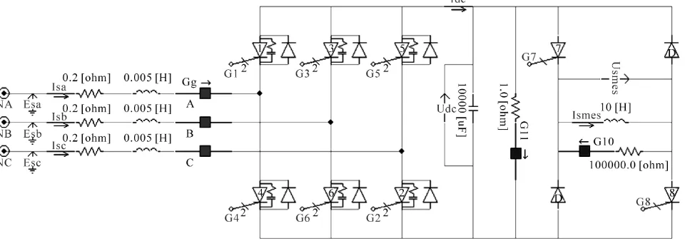
In the model shown as Figure 2, the 0.2 Ω resistance and the 0.005 Ω inductance are used to simulate the line loss and the 10 H inductance is used to simulate the su-perconducting magnet. Es is the phase voltage at the joint of VSMES and the transformer. The voltage source con-verter employs the three-phase six-impulse bridge in-verter. The control pulse of GTO is G1~G6 in turn. Ac-cording to the control pulse signal produced by the target power, changing the amplitude and the phase of Es can realize the control of the power.
The power control system (PCS) of VSMES adopts double closed-loop serial control, including a voltage outer loop and a current inner loop. Since the direct cur-rent control strategy of curcur-rent inner loop is introduced, the dynamic response of VSMES is improved to a large extent and also the anti-disturbance ability. Through the d-q transform of three-phase voltage and based on the target tracing power, the current value in the d-q coordi-nate is obtained, moreover, the target current value needed to be regulated can be derived from the decoup-ling transform of the current above, which achieves the purpose of direct current control [4].
The chopper comprises two-quadrant chopping circuit which is reversible in voltage. It adopts bang-bang con-trol strategy and maintains the voltage of the support capacitor constant. The control of the converter aims at power controlling, while the control of the chopper aims at voltage invariableness which supports the capacitance.
In this way, it decreases the difficulty of dynamic match- ing between the convertor and the chop to a large extent.
4. The Initial Parameters Design of the
VSMES
When the disturbance occurs, the VSME can compensate the power system with the storing energy. And the stored energy, in other words the initial parameters of the VSMES decides its compensating capability. So, to de-sign the initial parameters of the VSMES is very impor-tant. The initial parameters include L, Ism_ref, Udc and ES.
Where L represents the pure inductance of the supercon-ducting magnet; Ism_ref is the value of initial magnet
cur-rent; Udc is the real time voltage the supports the
capaci-tance; ES is the voltage magnitude on AC side. 4.1 The Rule for Selecting L
Superconducting magnet in the superconductive state is equivalent to a pure inductance without resistance in the VSMES. The relationship between the current I, L and energy W is following:
2 1 2
W LI (1)
When L is constant, I is in direct proportion to W in (1). But the current carrying capacity of the SM limits the magnitude of I. Meanwhile, Equation (2) shows that the DC voltage on the SM and the SM current all limits the selecting of L.
smes smes
di
U L
dt
(2)
where Usmes is the DC voltage on the SM; ismes is the SM
current. Considering the above factors and the real SMES made by HUST, the L is setting for 10 H in this paper.
[image:2.595.61.541.531.700.2]4.2 The Rule for Selecting Ism_ref
Considering that the VSMES can compensate the three unbalanced power of the power system during the oscil-lating period which has the biggest oscillatory power, the reference value Ism ref _ of the VSMES can be fixed
according to the unbalanced power which must be com-pensated and the compensating time.
2 _ 1
2 sm ref E L I
(3)
where E is the energy which the VSMES stores and just can meet the need of the power compensating.
Supposing the max compensating power by the VSMES during the oscillating period which has the biggest oscil-latory power is Pmax; and the keeping compensating
time is t, it must have:
max
E P t
(4)
It must be pointed out that, when the unbalanced power of the power system likes the low frequency os-cillation showed in the Figure 3, E must be
max 2 2
E P t
(5)
Equations (3) and (4) both suppose that the VSMES keeps to supply the energy to the power system during all the compensating time. So, when the fault ends, the SM current is lowest. And the lowest current can be set as
Ism_min. Considering the energy loss during the
compen-sating and the loss energy is corresponding to the current
_ sm loss I
varied in the SM, the wanted Ism_refis:
_ _ _ min _
sm ref sm ref sm sm loss
I I I I (6)
In summary, the rule for selecting Ism_ref is (7). max
_
_ _ min
1
2 sm ref
sm ref ref sm loss
E P t
E L I
I I I I
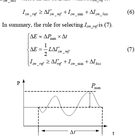
[image:3.595.63.289.475.706.2] (7) t max P
P
t PFigure 3. The curve of low frequency oscillation
where, Ism_min and Ism loss_ need artificially setting and
regulating according to the actual simulating result. And
Ism_min is very critical.
4.3 The Rule for Selecting Udc
In normal condition, the instantaneous adjustable output power by the VSMES meets (8).
2 2
sm sm dc smes
P Q U I (8)
where, Psm is the output active power by VSMES; Qsm
is the output reactive power by VSMES.
Along with the VSMES’s work, its adjustable instan-taneous power range gradually is also changing. When the VSMES absorbs energy from the power system, Ismes
up, UdcIsmes up, and the adjustable power range is bigger;
otherwise, when the VSMES supplies energy to the power system, Ismes down, Udc Ismesdown, and the
adjust-able power range is smaller. Meanwhile, the suitadjust-able allowance must be considered when selecting Ism_ref. If
the allowance is not enough, the VSMES cannot provide the needed power to the power system. In another word, the needed power exceeds the adjustable power range of the VSMES. This will cause the whole VSMES system crash. And Ism_min represents the allowance of Ism_ref
actu-ally. So, it is the reason why Ism_min is very critical. It
must meet (9).
2 2
_ min
sm sm dc sm
P Q U I (9)
According to the analysis above, supposing the system instantaneous power shortage which is needed to com-pensate is S, the rule for selecting Udcis (10).
_ min dc sm S U I
(10)
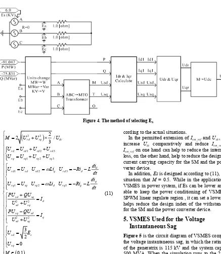
4.4 The Rule for Selecting ES
In order to ensure the power regulation of the VSMES in the controlled linear range, the signal modulation ratio M in the SPWM modulation must belong to 0 to 1. The relevant calculation of M is (11). And according to the
Udcand the P and Q which are the power needed to
out-put by the VSMES, ES can be got.
Maintaining M at 0.5, the corresponding ES can be got
by the method showed in Figure 4. It is difficult to de-duct ES directly from Udc according to (11). So the
in-verse method showed in Figure 4 is adopted. Presetting the ES, to calculate U'dc, and then compare it with the
setted Udc, judging its suitability by the setting ES. If U'dc
and Udc are more or less the same, then select the value
of ES; if U'dc and Udc are very different, then continue to
Figure 4. The method of selecting ES
2 2
1 2 3
1 2 3
1 2 3
1 2 3
2 2 2 2 2 2 / 3 3 2 0
rd rq dc
rd rd rd rd
rq rq rq rq
d
rd sd rd q rd d
q
rq sq rq d rq q
sd sq d sd sq sq sd q sd sq sd s sq
M U U U
U U U U
U U U U
di
U U U Li U Ri L
dt di
U U U Li U Ri L
dt PU QU I U U PU QU I U U U E U
0,1 M (11)4.5 Amendment of Ism_ref, Udc and ES
The above rules of the VSMES initial parameters are the basis general principles, which are based on the VSMES compensating the power system with equivalent three unbalanced power. But in the real applications of VSMES in power system, due to the existence of outer controller that is designed for achieving the set goals, under the control strategy of the outer controller, the compensating by the VSMES is not equivalent three un-balanced power compensating. Based on these circum-stances, it must adjust the values of Ism_ref and Udc,
ac-cording to the actual situations.
In the permitted extension of Ism_ref and Udc, it should
increase Udc comparatively and reduce Ism_ref. Lower Ism_ref on one hand can help to reduce the internal power
loss, on the other hand, help to reduce the design index of current carrying capacity for the SM and the power con-verter device.
In addition, Es is designed according to (11), under the situation that M = 0.5. While in the applications of the VSMES in power system, if Es can be lower and still be able to keep the power conditioning of VSMES in the SPWM linear regulate region , it can set a lower Es. This helps reduce the design index of the withstand voltage for the SM and the power converter device.
[image:4.595.64.501.72.575.2]5. VSMES Used for the Voltage
Instantaneous Sag
Figure 5 is the circuit diagram of VSMES compensating the voltage instantaneous sag, in which the rating voltage of the generatrix is 115 kV and the system capability is 500 MVA. When the simulation runs to the 21st s, the system fails for 0.75 s because of the three-phase ground- ing short circuit. During the 0.75 s, the bus voltage falls from 0.78 (p.u.) to 0.61, then recovers to 0.78.
If the system active power is abundant, VSMES merely need to provide enough reactive power for the system to compensate the voltage instantaneous sag. As
Figure 5. The circuit diagram of VSMES for compensating the voltage instantaneous sag
generate the reactive power control signal of the VSMES while the active power control signal remains zero [5-7].
According to the aforementioned design rules for the initial parameters of VSMES, the four initial parameters are setting as below:
The L is setting for 10 H. The support capacitance voltage of the VSMES is setting for 100 kV and the ini-tial current of the superconducting magnet is setting for 5 kA. The VSMES is connected to the system in parallel through the step-down transformer, and the secondary voltage of the transformer is 6 kV.
Figure 6 is simulation results of the bus voltage. Fig-ure 6(a) depicts real-time comparison curves of the bus voltage during the whole simulation. Figure 6(b) is tran-sient state comparison curves when the VSMES com-pensates for the voltage sag. Where Vpu_0 represents the system bus voltage without the availability of the VSMES, and Vpu represents the system bus voltage with the VSMES.
It’s obvious that the VSMES compensates the instan-taneous voltage sag of the system voltage favorably.
Figure 7 presents each monitoring variable of VSMES during the simulation. Figure 7(a) provides the real-time power changing curve of VSMES, in which the upper curve represents the active power Psm, and the lower curve represents the reactive power Qsm. Figure 7(b)
describes the superconducting magnet current. Figure 7(c) displays the voltage of the support capacitance.
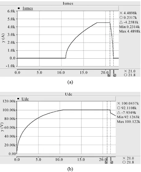
When the VSMES compensates the system voltage sag, it is found that the system needs about 125 MVar reac-tive power. Despite the fact that the VSMES is only modulating reactive power, the magnet current will de-cline due to losses of some components such as the con-vertor. In Figure 7(b), the magnet current declines from
(a)
(b)
Figure 6. The generatrix voltage. (a) Comparison graph of the generatrix voltage (p.u.); (b) Transient state comparison graph of the generatrix voltage(p.u.)
the original 5 kA to 1.8 kA during compensating. While
Figure 7(c) shows that the voltage of the support capaci-tance maintains invariable after magnetizing.
(a)
(b)
[image:6.595.57.289.81.497.2](c)
Figure 7. The monitoring variables of VSMES. (a) The real- time power of VSMES; (b) The superconducting magnet current; (c) The voltage of the support capacitance
in the end step when the VSMES compensates the volt-age decline and outputs 125 MVar reactive power, the magnet current declines to 1.8 kA, however, the mag- net current and the support capacitance voltage of 100 kV can still enable the VSMES adjust the reactive power of 125 MVar, and ensure that the compensating on the voltage sag keeps normal, avoiding the voltage collapse which supports the capacitance. Put it another way, the rules of the initial parameters design of the VSMES is feasible.
However, if the initial parameters are changed not ac-cording to the designed rules, for example: the initial current of the superconducting magnet is lowered to 4.5 kA, the support capacitance voltage will decrease when VSMES is compensating the voltage sag as Figure 8
(a)
[image:6.595.309.538.83.362.2](b)
Figure 8. The variables of VSMES after initial parameters changed. (a) The superconducting magnet current after initial parameters changed; (b) The voltage of the support capacitance after initial parameters changed
shows.
It’s obvious that the energy stored in the supercon- ducting magnet is not enough for the compensating. So it needs additional energy which supported by the support capacitance at the end of the compensating. Then the voltage of the support capacitance decreases. This will have negative effect on the control of VSMES. Therefore, the changed initial parameter is not reasonable. Mean-while it can be approved that the designed rules in this article are feasible and practical.
6. Conclusions
Based on the principle analysis of the VSMES, this paper establishes a time-domain simulation model of the VSMES with six-pulse and studies on the application of the VSMES in the power system.
To sum up:
1) On the basis of the detailed research on the opera-tional characteristics of the VSMES, the time-domain simulation model of the VSMES is established.
2) The initial parameters setting of the VSMES di-rectly determines the effects on the power system and involves the problem of the power range. This paper proposes a basic rule for parameters setting and uses an example to testify its feasibility.
the dynamic response is rapid, which is desirable for compensating the voltage sag of the system.
REFERENCES
[1] Y. Yang, “Development of Superconducting Technique and Its Application in Power System,” Power System Technology, Vol. 25, No. 9, 2001, pp. 48-60.
[2] Y. Shirai and T. Nitta, “On-line Evaluation of Power System Stability by Use of SMES,” IEEE Power Engi-neering Society Winter Meeting, New York, Vol. 2, 2002, pp. 900-905.
[3] Y. Ohsawa, Y. Maruoka, H. Takeno, et al., “Determina-tion of Installa“Determina-tion Loca“Determina-tion of SMES for Power System Stabilization,” Proceedings of the 2000 IEEE Interna-tional Symposium on Circuits and Systems, Geneva, 2000, pp. 233-236.
[4] Y. Li, S. J. Cheng, Y. Pan and Y. J. Tang, “Time Domain Simulation of the Characteristics for a Voltage Source Converter Fed SMES,” Automation of Electric Power Systems, Vol. 26, No. 18, 2002, pp. 60-63.”
[5] X. Liu, X. G. Zhu, X. Chu and X. H. Jiang, Voltage Sag Compensation by SMES,” Automation of Electric Power Systems, Vol. 28, No. 3, 2004, pp. 40-44.
[6] H. Zhang, P. C. Zhu, Y. Kang and J. Chen, “Improving Damping of Generator using Superconducting Magnetic Energy Storage Systems,” Power Electronics, Vol. 37, No. 1, 2003, pp. 50-53.