www.elsevier.com/locate/superlattices
Silicon-based ion channel sensor
M. Goryll
a,∗, S. Wilk
a, G.M. Laws
a, T. Thornton
a,
S. Goodnick
a, M. Saraniti
b, J. Tang
c, R.S. Eisenberg
caDepartment of Electrical Engineering, Arizona State University, Tempe, AZ 85287, USA
bDepartment of Electrical and Computer Engineering, Illinois Institute of Technology, Chicago, IL 60616, USA cDepartment of Molecular Biophysics and Physiology, Rush Medical College, Chicago, IL 60612, USA
Available online 20 April 2004
Abstract
In this paper we present a method to fabricate an aperture in a silicon wafer that can be used to suspend a freestanding lipid bilayer membrane. The design offers the feature of scalability of the aperture size into the submicron range. Lipid bilayer membranes formed across the aperture in the oxidized silicon substrate show a gigaohm sealing resistance. The stability of these membranes allowed the insertion of a nanometer-sized ion channel protein (OmpF porin) and the measurement of voltage dependent gating that can be expected from a working porin ion channel.
© 2004 Elsevier Ltd. All rights reserved.
Keywords: Biosensors; Lipid bilayers; Silicon devices
1. Introduction
The integration of biosensors with silicon-based readout circuits is a field of current interest. By combining detection of biochemical reagents and signal processing on a monolithic chip, sensors can be made much more versatile and robust. The crucial point in the fabrication of such a sensor is the biochemical detection mechanism. Here, gated ion channel proteins inserted in lipid bilayer membranes could serve as signal transducers that allow the detection of a change in ionic current when a biochemical agent is present. Ion channels have the advantage of being highly selective while being extremely sensitive. Atomic events (binding of an ion) are converted into a macroscopic signal, and a current of picoamps flows from one macroscopic reservoir to another, just as field effect transistors convert the ‘binding’ of a small charge on a gate into a macroscopic current from
∗Corresponding author. Fax: +1-480-965-8118.
E-mail address: [email protected] (M. Goryll).
The latter point is the reason why silicon was chosen as the substrate over glass [12–14]. While similar approaches use a silicon nitride layer as support [8–10], our process provides electrical isolation using only silicon that is thermally oxidized after the aperture has been etched. We will show that a lipid bilayer suspended across such an aperture forms a gigaseal even without the necessity for specific surface treatment of the silicon [10,11]. These bilayers allow the measurement of the behavior of an OmpF porin ion channel inserted into the membrane.
2. Experimental
Samples were prepared using 2 Si(001) substrates having a thickness of 270 µm. The substrates were patterned using photolithography. To protect the silicon during the subsequent etch process, a 2.4µm thick positive photoresist (AZ 4330) was used. The resist was exposed by a UV laser-based direct writing system (Heidelberg Instruments DWL66) that allows backside substrate alignment. The samples were etched in a deep Si reactive ion etcher (STS Advanced Silicon Etcher) using the Bosch process [16]. After etching, a thermal oxidation step followed to produce an electrically insulating layer on the surface. To decrease the capacitance of the samples in the measurement setup, a 50µm thick SU-8 photoresist (epoxy) layer was spun on the back side of the chip.
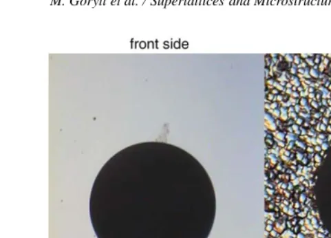
Fig. 1. Optical micrograph of the polished front and non-polished (rough) back side of a wafer with a hole etched using the deep Si reactive ion etch process. This process exhibits a good uniformity and no size enlargement during the etch process. This aperture has been used for lipid bilayer experiments.
the slope of the current trace. Current and bilayer capacitance were measured using an Axon Instruments Axopatch amplifier in connection with the pClamp software. The for-mation of a lipid bilayer was checked by comparing the data on resistance and capacitance with previously recorded values from bilayer chamber measurements. We also checked to see if the layer formed could be broken by the application of a short voltage pulse with
Vpulse >0.2 V. If the bilayer could not be broken by a voltage pulse and the capacitance was lower than expected, we rejected the preparation, thinking a bimolecular lipid layer had not been formed. The lipid blob was removed and another attempt was made. Ion channels were inserted into the membrane by adding OmpF porin to the ground bath.
3. Results and discussion
First samples were prepared with an aperture of 250µm diameter etched all the way through the silicon substrate. The aperture diameter was chosen to be large and resemble the size of commercially available bilayer chambers made out of PTFE or similar plastic material [17]. Because the aspect ratio of the aperture affects the formation probability as well as the stability of the bilayer film [18], an aspect ratio close to 1 was our goal. Using 2 wafers with a thickness of 275µm allowed the 250µm hole to be etched without the need to thin down the substrate using either dry or wet chemical silicon etching in a separate process step.Fig. 1shows the polished front side as well as the non-polished back side of an etched sample.Fig. 1shows that the hole exhibits an excellent uniformity and smooth vertical sidewalls. Concerning the surface roughness, no influence on bilayer formation is expected.
clearly indicates that a gigaseal between the lipid bilayer and the silicon support could be established. The capacitance associated with the lipid layer suggests that in this case a true bilayer was formed. After the measurement the bilayer could be broken by a brief high voltage pulse. The rise of the I –V curve at low voltage and the current offset at V =0 are due to capacitive charging of the bilayer which leads to a voltage offset shown ‘raw’. No compensation has been used.
The bilayers formed across these apertures were stable enough to allow the measurement of the insertion of an OmpF porin ion channel into the bilayer.Fig. 2(b) shows the current response of this voltage gated ion channel inserted into the bilayer membrane. This response is what is expected from the channel being inserted into a bilayer suspended across an aperture. Thus we were able to show that a micrometer sized aperture in silicon is capable of suspending a lipid bilayer as a host membrane for the insertion of a nanometer-scale ionic channel protein showing its regular properties.
Our procedure is successful but not efficient, or perfect. Several painting attempts had to be made until the desired result could be achieved. Also the bilayer resistance measured on the membrane reported inFig. 2(b) is significantly lower than that measured inFig. 2(a). We imagine that these problems are associated with the surface energy of the oxidized silicon used as the substrate material. An indirect measure of the surface energy of a material is the contact angle between a water droplet and the surface of the respective substrate [19]. PTFE and the plastic materials used for traditional bilayer chambers have hydrophobic surfaces, i.e. large water contact angles. The silicon dioxide used here, however, is not hydrophobic. It is easily wet by water and has a small water contact angle. The contact angle between the bilayer torus region and the substrate is sigificantly different from that in a bilayer in PTFE. The probability of bilayer formation is thought to be sensitive to wetting properties. Other laboratories even report that they were unable to form bilayers across silicon dioxide supports without changing the surface properties [10, 11]. Thus we will further investigate modification of the surface in the bilayer attachment region of the substrate.
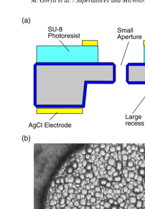
Fig. 3. (a) Schematic cross section through the aperture. (b) Small hole (diameter 150µm) etched inside a thinned recess. Both recess and small hole have been prepared by reactive ion etching. The visible roughness is due to the non-polished back side of the wafer. The original structure gets transferred during the deep etch process.
optical micrograph of the wafer back side with a 150µm aperture etched inside a 1 mm wide recess. The substrate has been thinned down to 170 µm inside that recess. Future downscaling of the bilayer support into the submicron range seems feasible.
4. Conclusions
[image:6.612.112.348.78.416.2]Measurements of the sealing resistance of a lipid bilayer attached to a 250µm wide silicon aperture show that a gigaseal could be achieved. Subsequently an OmpF channel protein could be inserted into this membrane. The corresponding I –V curve shows the expected voltage dependent gating action from a working porin ion channel.
While the initial aperture size is still in the micrometer range, the process used here allows a reduction of the aperture size even to submicron diameter. To preserve an aspect ratio of 1 the substrate around the aperture has to be thinned down. We present a design and proof of concept of the feasibility of this fabrication process. Varying hole size will allow study of the stability of the membrane and of the mechanisms governing the noise from a lipid bilayer. As the lipid bilayer acts itself as an inert substrate, the response of single nanometer-size ion channels can be detected, thus making this sensor a true nanoscale device.
References
[1] M. Trojanovicz, Fresenius J. Anal. Chem. 371 (2001) 246.
[2] W.F. Wonderlin, A. Finkel, R.J. French, Biophys. J. 58 (1990) 289–297.
[3] M. Eray, N.S. Dogan, L. Liu, A.R. Koch, D.F. Moffet, M. Silber, B.J.V. Wie, IEEE Trans. El. Dev. 40 (1993) 2137–2138.
[4] A. Ottova, V. Tvarozek, J. Racek, J. Sabo, W. Ziegler, T. Hianik, H.T. Tien, Supramol. Sci. 4 (1997) 101–112. [5] R.F. Costello, I.R. Peterson, J. Heptinstall, D.J. Walton, Biosensors Bioelectron. 14 (1999) 265–271. [6] S.D. Ogier, R.J. Bushby, Y. Cheng, S.D. Evans, S.W. Evans, A.T.A. Jenkins, P.F. Knowles, R.E. Miles,
Langmuir 16 (2000) 5696–5701.
[7] Y. Cheng, R.J. Bushby, S.D. Evans, P.F. Knowles, R.E. Miles, S.D. Ogier, Langmuir 17 (2001) 1240–1242. [8] J.E.M. McGeoch, M.W. McGeoch, D.J.D. Carter, R.F. Shuman, G. Guidotti, Med. Biol. Eng. Comput. 38
(2000) 113–119.
[9] C. Schmidt, M. Mayer, H. Vogel, Angew. Chem. Int. Ed. 39 (17) (2000) 3137.
[10] M.C. Peterman, J.M. Ziebarth, O. Braha, H. Bayley, H.A. Fishman, D.M. Bloom, Biomed. Microdev. 4 (2002) 231.
[11] R. Pantoja, D. Sigg, R. Blunck, F. Bezanilla, J.R. Heath, Biophys. J. 81 (2001) 2389. [12] N. Fertig, M. Klau, M. George, R.H. Blick, J.C. Behrend, Appl. Phys. Lett. 81 (2002) 4865. [13] N. Fertig, R.H. Blick, J.C. Behrends, Biophys. J. 82 (2002) 3056–3062.
[14] N. Fertig, C. Meyer, R.H. Blick, C. Trautmann, J.C. Behrends, Phys. Rev. E 64 (2002) 40901-1–40901-4, Rapid Comm.
[15] M. Mayer, J.K. Kriebel, M.T. Tosteson, G.M. Whitesides, Biophys. J. 85 (2003) 2684–2695. [16] A.A. Ay´on, R. Braff, C.C. Lin, H.H. Sawin, M.A. Schmidt, J. Electrochem. Soc. 146 (1999) 339–349. [17] Warner Instruments, Inc., Hamden, CT, USA,http://www.warneronline.com.
[18] S.H. White, Biophys. J. 12 (1972) 432.