Development and characterisation of pressed packaging solutions for
high-temperature high-reliability SiC power modules
J. Ortiz Gonzalez
a,⁎
, A.M. Aliyu
b, O. Alatise
a, A. Castellazzi
b, L. Ran
a, P. Mawby
a aSchool of Engineering, University of Warwick, Coventry, United Kingdom
bPower Electronics, Machines and Control Group, University of Nottingham, Nottingham, United Kingdom
a b s t r a c t
a r t i c l e i n f o
Article history:
Received 29 June 2016 Accepted 8 July 2016
Available online 18 September 2016
SiC is a wide bandgap semiconductor with better electrothermal properties than silicon, including higher tem-perature of operation, higher breakdown voltage, lower losses and the ability to switch at higher frequencies. However, the power cycling performance of SiC devices in traditional silicon packaging systems is in need of fur-ther investigation since initial studies have shown reduced reliability. These traditional packaging systems have been developed for silicon, a semiconductor with different electrothermal and thermomechanical properties from SiC, hence the stresses on the different components of the package will change. Pressure packages, a pack-aging alternative where the weak elements of the traditional systems like wirebonds are removed, have demon-strated enhanced reliability for silicon devices however, there has not been much investigation on the performance of SiC devices in press-pack assemblies. This will be important for high power applications where reliability is critical. In this paper, SiC Schottky diodes in pressure packages have been evaluated, including the electrothermal characterisation for different clamping forces and contact materials, the thermal impedance eval-uation and initial thermal cycling studies, focusing on the use of aluminium graphite as contact material.
© 2016 The Authors. Published by Elsevier Ltd. This is an open access article under the CC BY license (http://creativecommons.org/licenses/by/4.0/). Keywords:
SiC
Aluminium graphite Pressure packaging
1. Introduction
Power device packaging involves intimate contact between different materials with different thermomechanical properties. Coefficient of Thermal Expansion (CTE) mismatch between the semiconductor, the die attach and the baseplate causes thermomechanical stresses which increase the thermal resistance and junction temperature of the device under power cycling. The wirebond to source/gate metal interface is an-other reliability concern due to the occurrence of wirebond lift-off. Cur-rent packaging systems have been developed for silicon rather than silicon carbide hence, the different thermomechanical properties of SiC lead to different stresses on the elements of the packaging system. This results in a reduced power cycling capability of the current SiC de-vices compared with their silicon counterparts[1].
A packaging alternative where the elements of the packaging sub-jected to thermomechanical stresses are removed, achieving an en-hanced reliability, is the press-pack modules[2]. Press-pack modules also improve the system fault tolerance by failing to short. Press-pack modules have typically been used in high power applications like HVDC line-commutated converters where series connected thyristors are required for high DC voltage blocking capability. Press-pack IGBTs have been demonstrated by ABB and IXYS. Hence, voltage source
converter technology in press-pack is possible. In a press-pack module, the semiconductor is pressed between two copper heatsinks/electrodes, using an intermediate thermal contact to match the CTE. The weak ele-ments of the packaging system (solder and wire bonds) are removed thus achieving enhanced reliability, despite the more complex assembly system. There are few studies on the implementation of SiC in press-pack[3,4], however, the availability of larger SiC dies and the limited re-liability shown by the traditional packaging systems suggest that SiC press-pack modules could be a suitable alternative, particularly consid-ering the enhanced power cycling capability demonstrated in[4]. A pro-totype for the evaluation of a SiC Schottky diode in pressure packages is presented inSection 2. Here, aluminium graphite as an alternative con-tact material to molybdenum and DC heating measurements are pre-sented. The thermal impedance of this packaging system, considering different forces and different contact materials, is evaluated inSection 3with initial power cycling results presented inSection 4.Section 5 con-cludes the paper.
2. Prototype for the evaluation of silicon carbide devices in press-pack
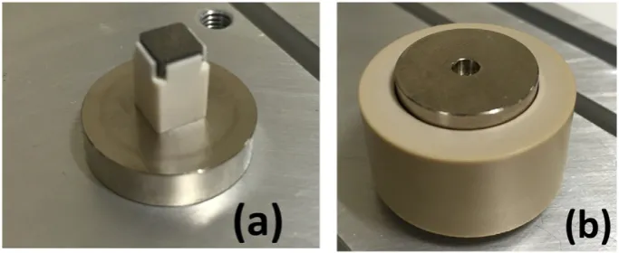
A prototype for the evaluation of a single 1200 V/50 A SiC Schottky diode (CPW5-1200-Z050B from Wolfspeed) on press-pack has been de-veloped and it is shown inFigs. 1 and 2. A die carrier made of PPS is used for positioning the die and the intermediate contacts used for matching ⁎ Corresponding author.
E-mail address:[email protected](J. Ortiz Gonzalez).
http://dx.doi.org/10.1016/j.microrel.2016.07.062
0026-2714/© 2016 The Authors. Published by Elsevier Ltd. This is an open access article under the CC BY license (http://creativecommons.org/licenses/by/4.0/).
Contents lists available atScienceDirect
Microelectronics Reliability
the CTE of the semiconductor. An external case made of PEEK is used for aligning the copper poles. PPS and PEEK are both engineering plastics, dimensionally stable with a temperature of operation over 200 °C. The evaluated prototype is not hermetic, hence the maximum operating voltage would be limited.
The size of the CPW5-1200-Z050B Schottky diode die is 4.9 mm × 4.9 mm with a thickness of 380μm. The dimensions of the in-termediate contacts are 3.7 mm by 3.7 mm for the anode contact and 4.9 mm by 4.9 mm for the cathode contact. The intermediate contacts have a thickness of 1.5 mm and have been machined with a radius of 0.5 mm, with a pressed area of 13.48 mm2and 23.80 mm2. According to[2], the usual clamping force for optimal electrical and thermal con-tact ranges from 10 to 20 N/mm2and for the studies on a single chip presented on this paper clamping forces of 300 N and 500 N have been selected.
The traditional material for the intermediate contacts is molybde-num, but aluminium graphite (ALG), a metal matrix composite by Schunk Hoffmann[5], appears as a suitable alternative. The properties of ALG2208, anisotropic material, compared with molybdenum and sil-icon carbide[1,5,6]are shown inTable 1.
With a suitable CTE and a high thermal conductivity[5], the electro-thermal performance of this alternative material is going to be evaluat-ed in this paper. A picture of the ALG contact, where the aluminium and graphite structure is easily identified, is represented inFig. 3.
2.1. Analysis of the electrical and thermal characteristics using pressure contacts
A simplified electrical model of the press-pack diode is represented inFig. 4and the thermal model can be represented using a basic Cauer network, as it has been done in[7]for a press-pack IGBT module.
The electrical resistance of a conductor is determined by Eq.(1), where ρis the resistivity of the material,dthe thickness andAthe cross section of the material.
R¼ρAd ð1Þ
The electrical contact resistance can be determined using the Eq.(2) [6].
RContact1−2¼ρ1þρ2
4 ffiffiffiffiffiffiffi πH
F
r
ð2Þ
whereρ1andρ2are the resistivity of the materials in contact,Hthe hardness of the softer material andFthe applied force. The thermal re-sistances and capacitances are determined by Eqs.(3) and (4), whered
is the thickness of the material,Athe cross section of the material,λth the thermal conductivity,cheatthe thermal capacity andρthe density of the material.
RTH¼ d
λthA ð
3Þ
CTH¼cheatρdA ð4Þ
The thermal contact conductance, assuming negligible radiation heat transfer[6,8]is determined by Eq.(5), whereksis the mean ther-mal conductivity,σthe effective root mean square of surface roughness,
mthe mean absolute surfaceflatness,Pthe contact pressure andHCthe contact microhardness.
hc¼1:25ks m
σ
P HC
0:95
ð5Þ
[image:2.595.82.255.59.173.2]These equations show the impact of the roughness andflatness of the surfaces in contact on the electrical and thermal contact[4]. For Fig. 1.Cross-section of the prototype.
[image:2.595.312.562.76.163.2] [image:2.595.131.473.586.726.2]this study the contacts have not been plated, hence the surface charac-terisation of the non-plated molybdenum and ALG contacts is shown in Figs. 5and6. The average surface roughnessSAis 0.763μm for the mo-lybdenum contacts and 0.736μm for the ALG contacts. Despite having a similar average surface roughness, inFig. 6the effect of the different ma-terials composing the ALG structure can be observed.
2.2. Initial measurements and considerations
The initial evaluation of the electrothermal properties of the press-pack diode has been done using a traditional DC power cycling test set-up where the calibrated forward voltage at low currents is used for estimating the junction temperature[9]. Box clamps BX-42, rated at 300 N and 500 N, and a heatsink model PS260/150B, both from GD Rectifiers, are used for these DC heating tests.
Fig. 7shows the forward voltage at high current during the heating of the diode, where the effect of the contact material on the forward voltage can be seen. ALG has a higher resistivity, hence the forward volt-age is higher when ALG contacts are used.
The effect of the clamping force on the forward voltage using ALG as contact is presented onFig. 8. According to Eq.(2)and the schematic shown inFig. 4, increasing the clamping force reduces the contact resis-tance, hence it reduces the voltage drop across the press-pack diode. For a heating current of 30 A the slope of the voltage during the heating has reduced slightly, suggesting a higher thermal conductivity when the clamping force is increased, as Eq.(5)indicates.
The thermal response for ALG and molybdenum contacts for differ-ent DC heating currdiffer-ents and a clamping force of 500 N is shown inFig. 9.
3. Thermal impedance characterisation
The transient thermal response shown inFig. 9is caused by the dif-ferent thermal impedance of the ALG and molybdenum contacts, as the
measurements and the analytical equations onSection 2show. The im-pact of the contact material and the clamping force is going to be evalu-ated in this section using a dedicevalu-ated thermal impedance characterisation equipment that is capable of performing power cycling and reliability evaluation on a module by extracting the impact of thermomechanical stresses on the transient thermal impedance of the module[10].
The thermal impedance which is a function of the thermal transient can be transformed into a graphical representation of the structure called the structure function[11]. The structure functions are obtained by direct mathematical transformations from the heating or cooling curves[12]. The structure function uses the thermal resistances and ca-pacitances in the Cauer form (because Cauer networks have a link with the physical structure) to identify changes in the structure of the device. There are two types of the structure function, differential and cumula-tive structure function. In[13]the differential structure functionK(RΣ)
is defined as the derivative of the cumulative thermal capacitance with respect to the cumulative thermal resistance.
K Rð Þ ¼Σ dCΣ
dRΣ ð6Þ
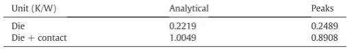
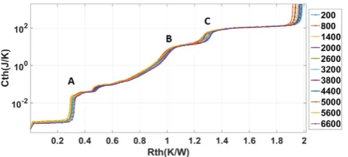
[image:3.595.312.543.53.212.2] [image:3.595.36.284.53.238.2]The differential structure function is used inFig. 10to analyze the two contacts at the same clamping force (500 N). The x-axis is the cu-mulative thermal resistance and the y-axis a function of the cucu-mulative thermal capacitance. To help understand the relationship betweenFig. 10and the physical structure, an analytical calculation using Eq.(3) was carried out to get an approximate resistance of the die and the con-tact. In the differential structure function the local peaks indicate a new interface in the heatflow path, hence from the location of the peaks and Fig. 3.Surface of the ALG contact.
Fig. 4.Equivalent electrical model of the press-pack diode.
[image:3.595.303.540.572.731.2]Fig. 5.Surface roughness of the molybdenum contact.
[image:3.595.35.292.634.727.2]the analytical values shown inTable 2the relationship between the structure andFig. 10has been deduced.
InFig. 10it can be observed that the die region for both ALG and mo-lybdenum is the same, as the same force and the same die are used. An increased thermal resistance in molybdenum is observed after the die region. The total difference between the two contacts is a thermal resis-tance of 0.339 K/W. This means that for the same power an assembly with ALG will run at lower temperature. This gives ALG an advantage of high power density. For the same material (ALG), different clamping forces were implemented and the differential structure function mea-sured. FromFig. 11it can be seen that 500 N gives a better thermal per-formance as the different materials are in better contact.
4. Power cycling results
The press pack was put under power cycling using constant current of 30 A to produce a change in the junction temperature during cycling (ΔTJ) of about 70 °C with a period of 60 s and a duty cycle of 0.5[9]. One of the determinants of the number of cycles is theΔTJ, as the number of cycles to failure is indirectly proportional to theΔTJ. The maximum junction temperature (TJmax) for this test is 90 °C and the minimum (TJmin) is 16 °C.Fig. 12shows the maximum junction temperature, the delta T and the minimum junction temperature.
InFig. 12repetitive spikes can be observed. This is due to the fact that after every two hundred cycles the thermal impedance of the de-vice is measured and transformed into the cumulative structure func-tion and the differential structure funcfunc-tion. The cumulative structure function is sum of the thermal capacitances (cumulative thermal
capacitance) in the function of the sum of the thermal resistances (cu-mulative thermal resistance) of the thermal system, measured from the point of excitation towards the ambient. Discretization of the struc-ture function results in a Cauer network. The slight dip in the minimum junction temperature and the maximum junction temperature is as a result of the changes in the ambient.
[image:4.595.82.254.51.200.2]The result of several measurements made during power cycling can be seen inFigs. 13and14. The differential structure function is repre-sented inFig. 13with no noteworthy difference in the measurements performed. The best way of observing these measurements is by using the cumulative structure function. As mentioned earlier, discretization of the structure function leads to a Cauer network. Hence, picking a point on the thermal capacitance axis is the same as picking a point in the structure of the device and obtaining its thermal resistance. This cannot be directly implemented with the differential structure function. By using this process on the cumulative structure function measure-ments shown inFig. 14the degradation on the power module can be ob-tained in form of the thermal resistance with respect to time.
[image:4.595.321.551.54.228.2]Fig. 7.Forward voltage during heating for different contact materials. Clamping forceF= 500 N.
[image:4.595.313.562.271.392.2]Fig. 8.Forward voltage during heating for ALG and different clamping forces (F= 300 N andF= 500 N).
Fig. 9.Junction temperature during heating. ALG and Mo as intermediate contacts, clamping force of 500 N.
Fig. 10.Differential structure for ALG (blue) and molybdenum (red) at the same clamping force (F= 500 N).
Table 2
Analytical and measured thermal resistances.
Unit (K/W) Analytical Peaks
Die 0.2219 0.2489
[image:4.595.82.256.576.717.2] [image:4.595.308.562.709.745.2]Three points in the cumulative structure function have been chosen to check for degradation. These points correspond to the points on cu-mulative structure function where there is a change in capacitance which corresponds to the peaks in the differential structure function. It can be seen inFig. 15that at the different interfaces there is no
noteworthy change in thermal resistance which means there is no deg-radation so far.
5. Conclusions
It has been shown in this work that although ALG has higher electri-cal resistivity it also has a lower thermal resistance than molybdenum. It means that for the same power ALG press pack design can be smaller (by reducing the size of the heatsink for example), also by using higher clamping force the electrical resistance and thermal resistance can be reduced. The preliminary cycling tests show no degradation and are still ongoing. A different failure mechanism is expected due to the ab-sence of solder, which is the predominant failure mode in SiC according to[1].
The future work entails the introduction of the solder layer between the die and the contact to reduce the contact resistance and thermal re-sistance. However that might have an effect on the reliability. Both an assembly with solder and no solder will be studied.
Acknowledgements
This work was supported by the UK Engineering and Physical Sci-ence Research Council (EPSRC) through the Underpinning Power Elec-tronics Devices Theme (EP/L007010/1), Components Theme (EP/ K034804/1) and HUB (EP/K035304/1).
References
[1] C. Herold, M. Schaefer, F. Sauerland, T. Poller, J. Lutz, O. Schilling, Power cycling ca-pability of modules with SiC-diodes, Integrated Power Systems (CIPS), 2014 8th In-ternational Conference on, Nuremberg, Germany 2014, pp. 1–6.
[2] J. Lutz, et al., Semiconductor Power Devices - Physics, Characteristics, Reliability, Springer-Verlag, 2011.
[3] Y. Sugawara, S. Ogata, et al., 4.5 kV 1000 A class SiC pn diode modules with resin mold package and ceramicflat package, Power Semiconductor Devices and IC's, 2008, ISPSD '08. 20th International Symposium on, Vol., No., 18–22 May 2008, pp. 267–270.
[4] V. Banu, P. Godignon, X. Perpiñà, et al., Enhanced power cycling capability of SiC Schottky diodes using press pack contacts, Microelectron. Reliab. 52 (9–10) (September–October 2012) 2250–2255.
[5] Schunk Hoffmann Carbon Technology AG,www.hoffmann.at.
[6] P. Rajaguru, H. Lu, C. Bailey, J. Ortiz-Gonzalez, O. Alatise, Electro-thermo-mechanical modelling and analysis of the press pack diode in power electronics, Thermal Inves-tigations of ICs and Systems (THERMINIC), 2015 21st International Workshop on, Paris 2015, pp. 1–6.
[7] C. Busca, R. Teodorescu, F. Blaabjerg, L. Helle, T. Abeyasekera, Dynamic thermal modelling and analysis of press-pack IGBTs both at component-level and chip-level, Industrial Electronics Society, IECON 2013 - 39th Annual Conference of the IEEE, Vienna 2013, pp. 677–682.
[8] M.M. Yovanovich, Four decades of research on thermal contact, gap, and joint resis-tance in microelectronics, IEEE Trans. Compon. Packag. Technol. 28 (2) (June 2005) 182–206.
[9] L.R. GopiReddy, L.M. Tolbert, B. Ozpineci, Power cycle testing of power switches: a literature survey, IEEE Trans. Power Electron. 30 (5) (May 2015) 2465–2473.
[image:5.595.38.286.53.167.2][10] www.mentor.com/products/mechanical/micred/t3ster.
[image:5.595.299.551.54.172.2]Fig. 11.Differential structure for ALG 500 N and 300 N.
Fig. 12.Power cycling parameters:TJmax(red),TJmin(yellow) andΔTJ(blue).
Fig. 13.Differential structure function for 6600 cycles.
[image:5.595.38.283.220.337.2]Fig. 14.Cumulative structure function for 6600 cycles.
[image:5.595.36.285.398.507.2] [image:5.595.35.287.611.725.2]