warwick.ac.uk/lib-publications
Manuscript version: Author’s Accepted Manuscript
The version presented in WRAP is the author’s accepted manuscript and may differ from the
published version or Version of Record.
Persistent WRAP URL:
http://wrap.warwick.ac.uk/122794
How to cite:
Please refer to published version for the most recent bibliographic citation information.
If a published version is known of, the repository item page linked to above, will contain
details on accessing it.
Copyright and reuse:
The Warwick Research Archive Portal (WRAP) makes this work by researchers of the
University of Warwick available open access under the following conditions.
Copyright © and all moral rights to the version of the paper presented here belong to the
individual author(s) and/or other copyright owners. To the extent reasonable and
practicable the material made available in WRAP has been checked for eligibility before
being made available.
Copies of full items can be used for personal research or study, educational, or not-for-profit
purposes without prior permission or charge. Provided that the authors, title and full
bibliographic details are credited, a hyperlink and/or URL is given for the original metadata
page and the content is not changed in any way.
Publisher’s statement:
Please refer to the repository item page, publisher’s statement section, for further
information.
Fig. 1 Impact of NBTI on the 3rd quadrant characteristics of a SiC
MOSFET. Cumulative negative HTGB stresses performed at 150 °C, as defined in [5]
Fig. 2 (a) VSD as a function of threshold voltage VTH during both PBTI and NBTI, (b) Normalized VTH as a function of the normalized VSD (measured
at ISD=50 mA) (Stresses defined in [5])
Characterization of BTI in SiC MOSFETs Using
Third Quadrant Characteristics
Jose Ortiz Gonzalez School of Engineering University of Warwick Coventry, United Kingdom [email protected]
Olayiwola Alatise School of Engineering University of Warwick Coventry, United Kingdom
Philip Mawby School of Engineering University of Warwick Coventry, United Kingdom [email protected]
Abstract—Bias Temperature Instability (BTI) is a
reliability concern for SiC MOSFETs which can have serious implications in the application if the true extent of the threshold voltage shift is underestimated. In this paper the third quadrant characteristics of SiC MOSFETs are used for characterizing the impact of accelerated gate stresses, evaluating the peak threshold voltage shift and tracking the recovery after stress removal. This method allows the evaluation of the impact of cumulative pulsed stresses of both long and short duration, which can be fundamental for characterizing the dynamics of BTI-induced threshold voltage shift in SiC MOSFETs under repetitive switching at the rated and accelerated gate voltage stresses.
Keywords—Bias Temperature Instability, SiC MOSFET
I. INTRODUCTION
Despite the improvements of the new generation SiC power MOSFETs, Bias Temperature Instability remains a reliability concern hence application engineers using SiC MOSFETs should take threshold voltage (VTH) shift into consideration. BTI is highly relevant to SiC MOSFETs due to a high density of oxide and interface traps at the SiC/SiO2
interface, as well as small band offsets due to the wider bandgap [1-4]. A peculiar characteristic of BTI in SiC is the recovery of VTH after stress removal. This recovery can mislead device engineers causing them to underestimate the true extent of the VTH shift after High Temperature Gate Bias (HTGB) stress. In high current applications where parallel connected SiC MOSFETs can be biased at negative gate voltages for long standby periods, loss of gate synchronization due to non-uniform VTH shift can cause electrothermal destruction from poor current sharing. The lack of recovery time after VGS bias in the application makes the standard reliability tests that allow recovery time unsuitable. It is therefore necessary to devise techniques for evaluating the VTH shift and recovery in real-time. This paper evaluates how a novel method for characterizing VTH shift caused by BTI presented by the authors in [5] can be used for evaluating cumulative stress pulses and capture phenomena that are not apparent during the conventional long stresses for BTI characterization.
II. BIAS TEMPERATURE INSTABILITY OVERVIEW AND
EXPERIMENTAL SETUP
BTI in SiC MOSFETs is a topic of interest, given the recent number of publications [1-4]. Depending on the polarity of the stress, the shift of VTH can be positive or
negative, giving either Positive Bias Temperature Instability (PBTI) or Negative Bias Temperature Instability (NBTI). Fundamental for evaluating the impact of BTI in SiC MOSFETs is capturing the peak VTH shift after the stress and the subsequent recovery once the stress is removed.
To that end, different methods have been proposed [1, 3], since the erroneous determination of the VTH shift can have negative consequences on the qualification of the devices. Using the methodology presented by the authors in [5], the peak shift and recovery of VTH after the stress removal can be detected. The methodology is based on 3rd quadrant characteristics of SiC MOSFETs. The threshold voltage shift caused by BTI affects the value of the source-drain voltage
VSD when VGS = 0 V. This is caused by the partial conduction of current through the channel when VGS=0 known as the body effect in SiC MOSFETs. Fig. 1 shows the measured 3rd
quadrant characteristics of a SiC planar MOSFET at ambient temperature which was subjected to highly accelerated negative HTGB stresses, using a high gate voltages at a temperature of 150 °C as defined in [5]. The 3rd quadrant
characteristics were measured at ambient temperature, after 16 hours relaxation at VGS=0, so as to characterize only the
[image:2.595.305.552.636.734.2]Fig. 3 Experimental setup for characterizing BTI shift using the 3rd
quadrant characteristics of a SiC MOSFET
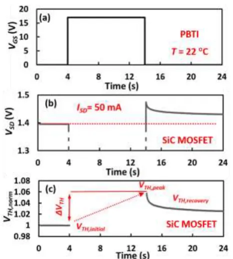
Fig. 4 Use of 3rd quadrant for BTI characterization: (a) Gate voltage
stress, (b) 3rd quadrant VSD voltage measured using ISD= 50 mA,
(c) Normalized VTH pre and after stress
Fig.5 Long duration repetitive stress pulses for evaluation of: (a) PBTI and (b) NBTI
permanent VTH shift caused by the stress.
Similar to the use of VSD as Temperature Sensitive Electrical Parameter (TSEP), using both positive and negative stresses a relationship between VTH and VSD can been defined. This is shown for the evaluated planar SiC MOSFET in Fig. 2, for a defined temperature (ambient) and a low value sensing current ISENSE of 50 mA (this is the current used to measure VSD during 3rd quadrant operation). As VSD is temperature dependent, it is important that ISENSE does not cause the self-heating of the device hence a suitable cooling method to minimize the impact of temperature is required. The normalized values are used to define a relationship between VSD and VTH, given by (1) [5].
,
1.02
,1.02
TH norm SD norm
V
V
(1)The test setup used here is similar to the test setup used for determining the junction temperature using VSD as TSEP [6] and it is shown in Fig. 3. It consists of a gate driving circuit used for stressing the gate oxide with a defined VGS stress and a current source which injects the sensing current
ISENSE flowing from source to drain. The stress timing signal
is generated using a waveform generator model TDS2024C from Tektronix, the transient VSD is measured using a differential probe model TA-043 from Pico Technology and captured using an oscilloscope model TDS5054B from Tektronix. The sensing current ISENSE is measured using a digital multimeter Fluke 175. Depending on the gate voltage used, ISENSE will flow: (a) through the channel only (positive
VGS which fully turns ON the device), (b) through the parasitic body diode (sufficient negative VGS) or (c) there is a current divider between the body diode and the MOSFET channel, due to the body effect and depending on VTH (VGS= 0 V). Using the calibration curve obtained in Fig. 2, for a known temperature the threshold voltage shift can be detected by measuring VSD.
Fig 4 shows the application of this technique. In this figure, the VGS stress (17 V) is shown in Fig. 4(a), together with the measured VSD in Fig. 4(b) and the calculated normalized VTH in Fig. 4(c) (equation (1) has been used for
VTH,norm calculation). Before the application of VGS (for t < 4 s), the measured VSD is 1.4 V (corresponding to nominal
VTH). During VGS stress application (4 s < t < 14 s), VSD falls to the ON-state resistance since the MOSFET is ON. After the VGS stress is removed (t > 14 s), VSD increases to a 6% higher value corresponding to increased VTH from PBTI due to negative charge trapping. Hence, the technique here shows
a 6 % increase in VTH due to a 10 s application of the rated
VGS. More details of the measurement technique for NBTI and PBTI are available in [5].
III. IMPACT OF REPETITIVE GATE STRESS PULSES ON BTI
[image:3.595.317.538.539.744.2] [image:3.595.51.277.580.748.2]Fig. 6 Measured VSD transient during the recovery transient after the first pulse. VGS=0. (a) PBTI, (b) NBTI
Fig. 7 Recovery of VTH-NORMALIZEDafter the stress pulse. (a) PBTI, (b) NBTI
Fig. 8 Normalized VTH shifts after cumulative pulsed stress tests (a) PBTI, (b) NBTI
A. Long duration repetivitve stresses
The impact of longer stress pulses and recovery times (in the range of minutes) was evaluated for both PBTI and NBTI stresses. The stress and characterization sequence is shown in Fig. 5(a) for the evaluation of PBTI and Fig. 5(b) for the evaluation of NBTI. The stress voltages are 22 V and -16 V for the PBTI and NBTI stresses respectively. The points where VSD was measured for tracking the peak shift and recovery of VTH after stress are identified from 0 (unstressed device) to 5 in Fig 5. The recovery transients (1-2) and (4-5) after each stress have been captured during 90 s.
The captured transient after the first pulse (1-2) is shown in Fig. 6(a) for the positive stress and Fig. 6(b) for the negative stress. As defined in the previous section and in more detail in [5], it is clearly observed how the positive stress shifts the measured VSD upwards due to the increased
VTH and the negative gate stress shifts the measured VSD downwards due to the reduction of VTH.
The recovery of VSD, thereby recovery of VTH, after the stress after the first pulse is clearly observed in both cases. Using (1) the normalized VSD value can be converted in the normalized VTH value and the recovery of VTH can be evaluated in more detail. This is shown in Fig 7 for both PBTI and NBTI stresses. For the device subjected to the positive stress the normalized increased of VTH is higher, with an increase of around 9 %, than for the device subjected to negative stress, with a reduction of around 4 %.
The recovery is faster for the positive stress than for the negative stress and for both recovery transients there is an initial segment where the measured VSD appears to be stationary. The authors attribute this to the transient response of the power supply during the change of conduction paths after the stress, when the voltage changes from low to high (PBTI) or high to low (NBTI).
The calculated VTH shift for the points defined in Fig. 5 is presented in Fig. 8. For both PBTI and NBTI stresses, it is clearly observed how after 30 minutes recovery at VGS=0, the
threshold voltage recovers to a value close to the pre-stress
[image:4.595.312.557.57.309.2]Fig. 9 (a) VSDduring PBTI pulsed stress tests. VSTRESS=22 V, VREC=0 V,
tSTRESS=2 s, tREC=2 s. ISENSE=50 mA, T=AMB (b) VSDduring NBTI pulsed stress tests. VSTRESS=22 V, VREC=0 V,
[image:5.595.308.541.58.158.2]tSTRESS=2 s, tREC=2 s. ISENSE=50 mA, T=AMB
Fig. 10 VSDduring PBTI pulsed stress tests. VSTRESS=35 V, VREC=0 V,
tSTRESS=2 s, tREC=2 s. ISENSE=50 mA, T=AMB
B. Short duration repetivitve stresses
From the results presented in section III.A it is clearly observed how the shift of VTH is more apparent for the first pulse and how it recovers exponentially after the stress removal. However, there is no information about the transient nature of the shift during the stress period. One of the main benefits of the presented characterization technique is that it will allow its evaluation using cumulative short stress pulses. This has been done for both negative and positive stresses in this paper. The stress time tSTRESS selected was 2 s, followed by a recovery time tREC of 2 s at VGS=0. The stresses were performed at the ambient temperature of 22 °C and the number of pulses was 40.
Fig. 9 shows the measured VSD transient for VSTRESS voltages of 22 V and -26 V. In both cases, an initial shift of
VSDcan be observed together with a partial recovery of VSD during the relaxation time of 2 s. As described in the section II, this recovery represents the recovery of VTH after the stress. Comparing Fig. 9(a) and Fig. 9(b), the rate of recovery is apparently higher for the positive stress, as the change of VSD is higher during the recovery phase of the pulsed stress. Comparing both stresses, a continuous reduction of VSD can be observed for the negative gate stress. Normalizing the peak VSD value and the variation of
VSD during the recovery, for the PBTI stress a total peak shift of +7.4 % with a recovery of -4 % during the 2 s recovery phase are observed, whereas in the case of NBTI, the peak shift is -8.4 % with a relative recovery of + 1.5 %. In the case of the negative pulsed stresses a continuous reduction of VSD can also be observed.
As BTI is also stress level dependent, another clear benefit of this method is that it allows to evaluate the impact on the VTH shift of highly accelerated stress voltages for short periods of time and its impact on shift and recovery. The same pulsed stress tests of period 4 s was performed using a stress voltage of 35 V, well above the nominal gate voltage of the evaluated planar device and the results are shown in Fig. 10, for a temperature of 22 °C. As the results in Fig. 10 show, during the initial phase of the 35 V pulsed stress, there is an initial VSD reduction indicating a reduction of VTH followed by the expected increase of VSD for PBTI
during the final stage of the pulsed stress. This phenomenon of dip and rebound was already described in [7] for Si MOSFETs and is caused by the different contribution of the oxide trapped charges (decreasing VTH) and the interface trapped charges (increasing VTH) during the different stages of the stress. This is defined by (2) [7], where Not is the stress-induced change in the oxide trapped charge, Nit is stress-induced change in the interface trapped charge and
COX is the specific gate oxide capacitance.
0
-ot it
TH TH
OX OX
qN
qN
V
V
C
C
(2)In a traditional long duration stress, this peculiar feature of the highly accelerated stress test would not be captured, hence the benefits of using the 3rd quadrant characteristics for
assessing the impact of the BTI in SiC MOSFETs.
IV. CONCLUSION
In this paper it has been shown how the third quadrant characteristics of SiC MOSFETs can be used for evaluating the VTH shift caused by BTI. It is shown how VSDis and effective cursor for detecting the peak shift of VTH and tracking the recovery of VTH after the gate stress is removed. The implementation of this method is similar to the use of
VSD as TSEP. Using short duration pulsed stress tests, the phenomenon of dip and recovery of VTH has been captured during initial stages of highly accelerated stress tests, hence demonstrating the importance that this methodology could have for characterizing BTI in SiC MOSFETs.
REFERENCES
[1] T. Aichinger, G. Rescher, and G. Pobegen, "Threshold voltage peculiarities and bias temperature instabilities of SiC MOSFETs," Microelectronics Reliability, vol. 80, pp. 68-78 January 2018 [2] A. J. Lelis et Al. "SiC MOSFET threshold-stability issues," Material
Science in Semicond Processing, vol. 78, pp. 32-37, May 2018 [3] D. B. Habersat, A. J. Lelis, and R. Green, "Measurement
considerations for evaluating BTI effects in SiC MOSFETs,"
Microelectronics Reliability, vol. 81,pp. 121-126, February 2018. [4] K. Puschkarsky, H. Reisinger, T. Aichinger, W. Gustin and T.
Grasser, "Understanding BTI in SiC MOSFETs and Its Impact on Circuit Operation," in IEEE Transactions on Device and Materials Reliability, vol. 18, no. 2, pp. 144-153, June 2018.
[5] J. A. Ortiz Gonzalez and O. Alatise, "A Novel Non-Intrusive Technique for BTI Characterization in SiC MOSFETs," inIEEE Transactions on Power Electronics. Early Access, pp. 1-1, 2018 [6] G. Zeng, H. Cao, W. Chen and J. Lutz, "Difference in Device
Temperature Determination Using p-n-Junction Forward Voltage and Gate Threshold Voltage," in IEEE Transactions on Power Electronics, vol. 34, no. 3, pp. 2781-2793, March 2019.
[image:5.595.53.288.530.725.2]![Fig. 2 (a) VSD as a function of threshold voltage VTH during both PBTI and NBTI, (b) Normalized VTH as a function of the normalized VSD (measured at ISD=50 mA) (Stresses defined in [5])](https://thumb-us.123doks.com/thumbv2/123dok_us/9426997.447151/2.595.313.544.204.339/function-threshold-voltage-normalized-function-normalized-measured-stresses.webp)