© 2019, IRJET | Impact Factor value: 7.211 | ISO 9001:2008 Certified Journal
| Page 7751
AN AUGMENTED LED MATRIX DISPLAY USING FPGA
Rajeshwari
1, Punit Ronad
21
PG student, Dept. of Electronics and Communication Engineering, M.Tech (VLSI & ES), Sharnbasva University,
Karnataka, India
2
Assistant Professor, Dept. of Electronics and Communication Engineering, M.Tech (VLSI & ES), Sharnbasva
University , Karnataka, India
---***---Abstract - Light emitting diodes (LEDs) are a unit used fornumerous applications like signboards, emotional lighting systems, building lightings, and façades. LEDs area unit non-toxic, mercury-free, consume low power and supply a protracted life. These advantages build LEDs terribly enticing lighting devices used for numerous lighting systems from emotional lighting systems to terribly massive lighting systems utilized in and on buildings. The LED-based show management unit plays a vital role during this victimization technology.
Key Words: Flickering, Led matrix, Intensity, Display
driver, FPGA, Beagle bone black.
1. INTRODUCTION
LED displays represent modernization of town and digital era, and catch on for its versatile application with many advantages. Compared to different ancient show technology (such as noble gas light-weight, fluorescent tubes, alphanumeric display) it's edges like high brightness, wide viewing angle, less energy consumption, long service life, wet resistance, hot cold resistance, etc. with affordable price. This sort of show, sculpted out by segmented or dot-matrix LEDs, are often of little, medium or massive size. Segmented display and dot-matrix displays square measure wide employed in electronic and medical instrumentality, instrument panels.
Although segmentation kind displays need
straightforward driving circuit, dot-matrix displays will generate characters of higher form of various languages facilitating each static and animated image-pattern. Thanks to charm for animated impact like scrolling and flying, promotional material and emergency info are often got regarding through LED dot-matrix show publicly places like train station, hospital, airport, bus stand, restaurant, super shop, bank, stock market etc.
An LED dot-matrix display consists of LED panel and driving circuit for row and column with straightforward x-y addressing. There are forms of scanning approaches controller and in depth process power. In present day, single chip microcontroller (SCM), CPLD (Complex Programmable Logic Device), FPGA (Field-Programmable Gate Array) at the side of different digital IC’s like latch, register etc. square measure accustomed change the information transmission path and management signal path in PCB layout. To style an
outsized LED dot-matrix show, we'd like to trot out unsteady and lower glowing intensity problems. Because the size of show becomes larger, to cut back perception of unsteady, frame rate and refresh rate got to be enhanced in each horizontal and vertical directions.
However, in spite of mistreatment quick digital controller, delays related to different digital electronic equipment, stray inductance and capacitance limit to the quantity of LED dot-matrix modules and refresh rate. A lot of to the purpose, just in case of huge board, information and management signal got to be transmitted long distance via long wire having massive inductance. Additionally to it, parallel long wires exhibit stray capacitance and coefficient of mutual induction generating interference impact between parallel wires that's bar to high speed information transmission in traditional configuration. At a similar time, although mistreatment information latch and register with driver to manage column states facilitates reducing variety of connecting wires between controller and board, it additionally introduces delay and will increase interval.
During this work, the show works at a rate bigger than one hundred scans per second and therefore the eye observe the show to be steady. If we tend to cut back the scan rate, every of the LEDs are often seen because the potency of this flow through the LEDs, lower frame rate (with same switch-on time) reduces overall glowing intensity.
2. EXISTING SYSTEM
Enhanced PWM method, based on approaching
PWM curve to DC curve and reducing the error gap between them. This make it suitable for hardware implementation on an FPGA platform.
Hardware become more compound and must use
more driver modules, which manipulate in energy utilization and price of system.
3. PROPOSED SYSTEM
3.1 THE FPGA
© 2019, IRJET | Impact Factor value: 7.211 | ISO 9001:2008 Certified Journal
| Page 7752
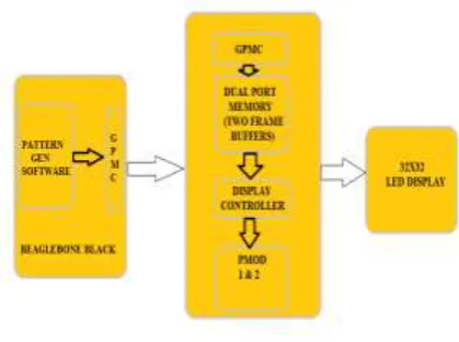
the BeagleBone Black processor unengaged to generate thepatterns and perform alternative tasks. As shown in Figure1 below, package running on the BeagleBone Black generates patterns. These patterns square measure fed to the FPGA on the LogiBone board exploitation the TI SOC’s GPMC bus. These patterns square measure written to a dual-port memory that is a show buffer. Finally a display controller reads the patterns out of the twin port memory, shifts the info into the show, and allows the row drivers as required to show the image. The complete method is recurrent regarding two hundred times per second and generates a 32x32 RGB image with 12-bit color with none interaction from the BeagleBone Blacks’ processor.
3.2 GPMC INTERFACE
[image:2.595.63.273.527.683.2]The TI SOC includes a programmable memory interface known as the all-purpose memory controller (GPMC). This interface is extraordinarily versatile. It will operate in each synchronous and asynchronous modes and also the bus temporal arrangement is programmable in 10ns increments. The GPMC bus are accustomed transfer element information from the package on the Beagle Bone Black to the FPGA on the LogiBone board. In the system, the GPMC is organized to work in its asynchronous, multiplexed address/data mode. During this mode, each the address and information buses square measure sixteen bits wide. This allows a whole 12-bit element to be transferred from the processor on the BBB to the FPGA on the LogiBone board in an exceedingly single write operation. The scan or write address is locked into a short lived holding register on the rising fringe of the GPMC_ADVN signal and also the write information is locked into its own temporary holding register on the falling fringe of the GPMC_WEN signal. This needs exploitation the GPMC_ADVN And an inverted version of the GPMC_WEN information signals as clocks.
Figure 1:Block diagram of the system including a block
diagram of the FPGA’s major functional blocks.
3.3 DISPLAY BUFFER
The show buffers area unit enforced victimization Xilinx Block RAMs designed as dual-port recollections with asynchronous browse and write ports. The primary RAM contains show buffers zero and one for the highest 1/2 the show. The second RAM contains show buffers zero and one for very cheap of the show. Structuring the recollections to contain the show every permits the pixels in rows zero to fifteen to be browse from memory on the precise same clock that the pixels in rows sixteen to thirty one area unit browse from memory.
3.4 DISPLAY DRIVER
The show driver reads component values from memory, shifts those values to the show, and cycles through the rows of the show as needed to implement binary coded modulation. The show driver is enforced as a state machine. Every state implements a step within the refresh method. Once that step is complete, the state machine moves to consecutive step within the method.
3.5 THE LED PANEL
The junction rectifier panel contains 1024 RGB LEDs organized during a matrix of thirty two rows and thirty two columns. Every RGB junction rectifier contains separate red, green, and blue junction rectifier chips assembled along during a single package. The show is divided horizontally into 2 halves. The top half of the panel consists of thirty two columns and sixteen rows and bottom half of the panel additionally consists of thirty two columns and sixteen rows shown in Figure 2.
The display’s columns area unit driven by one set of drivers and therefore the display’s rows area unit driven by another set of drivers. To illuminate associate junction rectifier, the drivers for each the column and therefore the row for that junction rectifier should be turned on. To vary the colour of associate junction rectifier, the red, green, and blue chips in every junction rectifier package area unit controlled singly and have their own column drivers. Figure 3 below may be a schematic illustration of the display’s column and row driver organization.
© 2019, IRJET | Impact Factor value: 7.211 | ISO 9001:2008 Certified Journal
| Page 7753
Figure 2 : RGB LED panel column and row driverorganization.
Figure 3: Column driver operation for the R0 data input and top-half red columns outputs.
Each of the drivers features a serial input data, a blanking input, a register, and a parallel output register as shown in Figure 3, information on the serial data input is shifted into the register victimization the spacecraft clock time signal. When a whole row of information has been shifted in to the register, the LATCH signal is employed to transfer the row of pixel data from the register into the parallel output register.
3.6 DRIVING THE PANEL:
The show is multiplexed and encompasses a 1/16th duty cycle. This implies that no quite one row out of the sixteen within the prime half the show and one row out of the sixteen within the bottom half the show are ever light promptly. Moreover, a crystal rectifier will solely get on or off. If each the row and column for a crystal rectifier are turned on, the crystal rectifier are going to be illuminated; otherwise, the crystal rectifier are going to be off. To show a picture, the whole crystal rectifier panel should be scanned quickly enough in order that it seems to show an eternal image while not a flicker. To show completely different colors and different brightness levels, the brightness of the
red, green, and blue crystal rectifier chips at intervals every crystal rectifier package should be adjusted by variable the quantity of your time that every crystal rectifier chip is on or off at intervals one refresh cycle.
The basic method accustomed refresh the show once mistreatment 3 bits-per-pixel color (one bit for red; one bit for green; and one bit for blue) is that the following:
1. Shift the picture element information for row zero into the highest column drivers and therefore the picture element information for row sixteen into the lowest column driver’s mistreatment the R0, G0, B0, R1, G1, and B1 information inputs and therefore the time shift clock signal.
2. Assert the blanking signal to blank the show.
3. Set the address input to zero.
4. Latch the contents of the column drivers‘ shift registers into the column drivers‘ output registers mistreatment the LATCH signal.
5. Deassert the blanking signal to show rows zero and sixteen.
6. Wait some mounted quantity of your time.
7. Repeat the method for every of the pairs of rows within the show.
8. Repeat the whole method a minimum of a hundred to two hundred times per second to stop flicker.
The on top of method uses one bit per crystal rectifier color. This may provide you with eight doable colours: black; the first colors red, green, and blue; the secondary colours cyan, magenta, and yellow; and white. To show a lot of colours and brightness levels the on top of technique is changed to use binary coded modulation. In binary coded modulation, every picture element is controlled mistreatment quite one bit per color per picture element. the quantity of your time every red, green, and blue crystal rectifier chip is on is then varied proportionately to the pixel’s red, green, and blue values.
In binary coded modulation, the subsequent method is performed to refresh the display:
1. Shift bit zero of every pixel’s red, green, and blue values for rows zero and sixteen into the column drivers.
2. Assert the blanking signal to blank the show.
3. Set the address input to zero.
[image:3.595.38.281.320.462.2]© 2019, IRJET | Impact Factor value: 7.211 | ISO 9001:2008 Certified Journal
| Page 7754
5. Deassert the blanking signal to show rows zero andsixteen.
6. Wait some quantity of your time, N.
7. Repeat the on top of method for ensuing higher order little bit of color information within the same row. In step 6, wait double the previous delay time. Repeat this method for every little bit of color information, doubling the delay time once displaying every serial bit.
8. Repeat the on top of method for every of the pairs of rows within the show.
9. Repeat the whole method a minimum of a hundred to two hundred times per second to stop flicker.
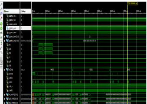
[image:4.595.301.565.60.239.2]4. RESULT
Figure 4: Simulation waveform.
4.1 DISPLAY DRIVER:
[image:4.595.37.291.303.483.2]For the control and data outputs for three rows worth of display data output, the basic process is to blank the display, latch in the previously shifted data, update the row selects, unblank the display, shift in the next set of pixel data, and then wait for an update timer to expire. This is repeated four times for each row. Notice that its low period doubles three times within the output period for each display row. This is the result of using binary coded modulation to vary the intensity of each pixel. shown in figure 5.
Figure 5 : simulation waveform of display driver.
5. ADVANTAGES AND APPLICATIONS
5.1 ADVANTAGES
The essential advantage is the looks of LEDs, that look too awe-inspiring.
2. It provides the slim screen with sleek style that is adjustable at anywhere.
3. LEDs are much better than alphanumeric display monitors as a result of they are doing not use fluorescent bulbs thanks to that they're lighter and diluents in weight.
4. LEDs consume less energy and save a great deal of power., wherever because the LCD’s use fluorescent bulbs thanks to that they consume a great deal of power.
5. LEDs give bright image quality by enhancing the distinction and enriching the vary of colours. The wavelength vary of lights used are specified to administer prime quality.
5.2 APPLICATIONS
The light-emitting diode matrix is helpful for each industrial or industrial show.
2. Digital serial system utilized in restaurants and hospitals.
3. Showing any quite data publicly place so on.
4. Play games, watch movies, show a dashboard of information.
6. CONCLUSION
© 2019, IRJET | Impact Factor value: 7.211 | ISO 9001:2008 Certified Journal
| Page 7755
show it to the light-emitting diode panel because it isprogrammed. The project additionally able to show image of four cascaded panel as per demand within the project scope.
7. FUTURE WORK
There are several admirations to improve the system, but admirations to time constraint, my very own information limitation and price constraint. The system can also browse date in SDRAM in format of .RGB, if this can be improved and also the system can show any format of image, user will simply take the image what they need to show and simply send it to be displayed.
REFERENCES
[1] I. H. Oh, ≪A single-stage power converter for a large screen LCD back-lighting,≫ chez in Proceedings of IEEE Applied PowerElectronicsConference and Exposition, March 2006.
[2] K. H. Loo, Y. M. Lai, S. C. Tan et C. K. Tse, ≪On the color stability of phosphor-converted white LEDs under dc, PWM, and bilevel drive,≫ PowerElectronics, IEEE Transactions on,
vol. 27, n° %12, p. 974–984, Feb 2012.
[3] A031E, ≪PWM vs analog dimming of LED,≫ Aimtec Inc, 2011.
[4] B. Ackermann, V.Schulz, C.Martiny, A.Hilgers et X.Zhu,
≪Control of LEDs,≫ chez in Record of IEEE Industry
Applications Conference, October 2006.
[5] P. Narra et D. S. Zinger, ≪An effective LED dimming approach,≫ chez in Record of IEEE Industry Applications Conference, October 2004. W. Kurdthongmee, ≪Design and implementation of an FPGA-based multiple colour LED
display board,≫ Microprocessors and Microsystems, vol.
29, p. 327–336, 2005.
[6] C. C. Chen, C. Y. Wu et T. F.Wu, ≪LED back-light
driving system for LCD panels,≫ chez in Proceedings of IEEE
Applied Power Electronics Conference and Exposition (APEC), Mars 2006.
[7] ,. Xilinx, ≪Spartan-3 FPGA Starter Kit Board User Guide,≫ [En ligne]. Available: www.xilinx.com.. [Acces le 15 03 2016].
[8] KingBright, ≪Data-sheet LED RGB,≫ 19 11 2016. [En ligne].
Available: