Evolution of Morphology of Nano-Scale CuO Grown on
Copper Metal Sheets in 5 wt% NaCl Solution of Spray Fog
Environment
Hao-Long Chen, Tsung-Hsun Chiang, Ming-Cheng Wu
Department of Electronic Engineering, Kao Yuan University, Kaohsiung City, Chinese Taipei. Email: [email protected]
Received July 1st, 2012; revised August 8th, 2012; accepted August 18th, 2012
ABSTRACT
Nano-scale copper oxide with various morphologies is synthesized via the thermal oxide method and growth in a 5 wt% NaCl solution of spray fog environment. The nano-scale copper oxide is grown on copper metal sheets via the thermal oxide method at 650˚C for 60 minutes. Nano-scale copper oxide grains and nanowires are induced on copper metal sheets then placed in 5 wt% NaCl solution of salt spray fog environment. Significant changes in particle size and mor-phology are observed with increasing salt spray fog treatement time. The mormor-phology of nano-scale copper oxide varies from nanograins to nanowires, Ctahedron, and icositetrahedron. The morphologies and structures of the obtained nano-scale copper oxide are investigated by scanning electron microscopy and energy-dispersive spectroscopy. Possible growth mechanisms are discussed.
Keywords: Nano; CuO; Morphology; NaCl Solution; Spray Fog
1. Introduction
Nanoscale one-dimensional (1D) and two-dimensional (2D) materials such as nanowires, nanorods, nanoribbons, and nanosheets have attracted a lot of interest due to their unique physical properties and potential applications in nanodevices.
Copper oxide (CuO) is a well known p-type semicon- ductor and a photovoltaic material. It has a narrow band gap (1.2 eV). CuO is desirable due to its availability and abundance of the starting materials, non-toxicity, and low production cost [1]. Consequently, it is widely used in applications such as catalysis [2], sensors [3], solar cells [4,5], and field-emission emitter materials [6]. However, the chemical and physical properties of CuO strictly de- pend on its size and morphology [7]. Many studies have synthesized various CuO nanostructures. A number of methods have been used to synthesize and control the size and morphology of nano-scale CuO, such as thermal evaporation [1], solution synthesis [7], thermal oxidation [8], sol-gel [9], hydrothermal method [10], electrospin- ning [11] and microwave hydrothermal synthesis [12].
These methods have been used to synthesize CuO nanomaterials with various morphologies, such as nano- particles, 1D nanowires, nanorods, and nanobelts; 2D nanosheets, nanoleaves, and nanowiskers; and three-dim- ensional peachstone-like, boat-like, and ellipsoid-like na-
nostructures [10]. The morphology of nano-scale CuO is related to growth environment conditions, in addition to processing methods.
In this work, nano-scale CuO with various morpholo- gies is synthesized via the thermal oxide method and growth in a 5 wt% NaCl solution of spray fog environ- ment. The morphology of nano-scale CuO varied from nanograins to nanosheets and nanoneedles with increase- ing salt spray fog treatement time. Possible growth mechanisms are discussed.
2. Experimental Procedure
CuO with various morphologies was synthesized via the thermal oxide method and growth in a 5 wt% NaCl solu-tion of spray fog environment.
Copper (99.99 wt% Cu) substrate samples with di- mensions of 10 mm (width) × 10 mm (length) × 1 mm (thickness) were prepared according to the following procedure: the substrate was polished with various grind- ing papers (400, 600, 800, 1200, 2000, and 4000 grade) and then ultrasonically cleaned with acetone, ethanol, and de-ionized water for 10 minutes sequentially to re- move the impurities and native oxides on its surface. The samples were then dried by blowing with high-pressure nitrogen gas.
a resistance-heated tube furnace in a pure oxygen at- mosphere at a temperature of 650˚C for 60 minutes. Nano-scale CuO grains were induced on the copper metal sheets and then placed in 5 wt% NaCl solution of spray fog environment. The treatment times of the sam- ples in the spray fog environment were 1, 7, 14, 21, and 28 days, respectively. The temperature of the spray fog environment was kept in 45˚C .
The surface morphology of the samples was observed using a scanning electron microscope (SEM, Hitachi S3000N, Japan) operated at 30 kV. The chemical com- position of the nanomaterials was confirmed by energy- dispersive X-ray analysis (EDX, Horiba, Japan). The phases and structure of the nanomaterials were identified by grazing-incidence X-ray diffraction (GIXRD) using a Rigaku D/MAX 2500 multipurpose X-ray thin-film dif-fractometer with monochromatic high-intensity CuK
radiation ( = 0.15418 nm).
3. Results and Discussion
3.1. Phase and Structure Analysis
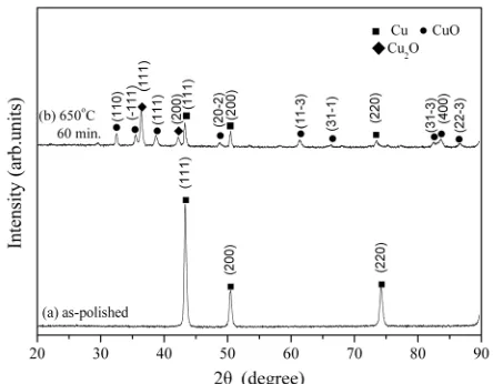
The X-ray diffraction patterns of polycrystalline Cu metal sheets prepared by polishing and thermal oxidation are shown in Figure 1. Figure 1(a) shows the diffraction
peaks of an as-polished Cu metal sheet, which are assigned to the (111), (200) and (220), planes of face-centered cubic (fcc) Cu. This result is in agreement with the standard data from JCPDS card No. 85-1326. The XRD patterns of CuO samples on Cu metal sheets prepared via thermal oxidation are shown in Figure 1(b). The XRD peaks can be indexed
as monoclinic structured CuO (JCPDS card No. 80-1917), cubic structured cuprous oxide (Cu2O) (JCPDS card No.
78-2076), and fcc Cu metal from the substrate (JCPDS card No. 85-1326). The diffraction peaks of the mono-clinic structured CuO are assigned to the (110), (–111), (111), (20-2), (11-3), (31-3), (400), and (22-3) planes. The peaks of cubic structured Cu2O are assigned to the (111)
and (200) planes.
Figure 2 shows the XRD patterns of nano-scale CuO
prepared via the thermal oxide method and then placed in a 5 wt% NaCl solution of spray fog environment for 0 (only thermal oxidation), 1, and 28 days, respectively. The diffraction pattern of the copper(II) chloride (CuCl2)
appeared for the sample prepared via thermal oxidation and then placed in a 5 wt% NaCl solution of spray fog environment for 1 day, in addition to the original produc- tion peaks of CuO, Cu2O, and Cu metal substrate (Figure 2(b)). The diffraction peak of the monoclinic structured
CuCl2 is assigned to the (–405) planes (JCPDS card No.
79-1635). The peaks of CuCl2 increased with increasing
salt spray fog treatment time. Figure 2(c) shows that the
diffraction planes of CuCl2 were (002), (111), (112),
[image:2.595.311.533.98.271.2](–313), and (–221) for the sample treated using 5 wt%
Figure 1. XRD patterns of polycrystalline Cu metal sheets prepared by (a) polishing and (b) thermal oxidation.
Figure 2. XRD patterns of nano-scale copper oxide pre-pared by thermal oxide method followed by exposure to 5 wt% NaCl solution of spray fog environment for (a) 0 (only thermal oxidation); (b) 1; and (c) 28 days.
NaCl solution of spray fog for 28 days.
The XRD results indicate that the main phases of the nano-scale CuO grown on pure Cu metal substrates after thermal oxidation were CuO and Cu2O. CuCl2 was in-
duced on pure Cu metal substrates when the samples were placed in 5 wt% NaCl solution of spray fog envi- ronment.
3.2. Morphology Observation
Figure 3 shows the surface morphology of polycrystal-
line Cu metal sheets prepared by polishing. The surface of the Cu metal sheets did not have any surface chemical products.
[image:2.595.310.535.314.494.2]Figure 3. Surface morphology of polycrystalline Cu metal sheet prepared by polishing.
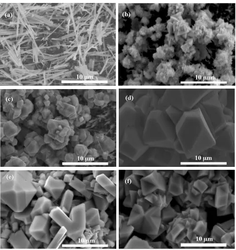
grown via thermal oxidation on Cu metal sheets for 60 minutes at 650˚C are shown in Figure 4(a). The mor-
phologies of nano-scale surface products formed after thermal oxidation followed by exposure to 5 wt% NaCl solution of spray fog environment for various durations significantly change, as shown in Figures 4(b)-(f). Fig- ure 4(a) shows Ctahedral-shaped grains about 1 μm ag-
gregated on the nanowire after 1 day in a 5 wt% NaCl solution of spray fog environment. The Ctahedral-shaped grain size increased with increasing spray fog treatment time. The Ctahedral-shaped grains are replaced by a six- horn-shaped icositetrahedron. Each crystal has six apexes, each of which is connected to four sides to form an ico- sitetrahedron [13]. Icositetrahedron-shaped crystals can be observed in the Figure 4(d). When the salt spray fog
treatment time was increased to 28 days, the edges and corners of the icositetrahedron-shaped crystals become more extrusive (Figure 4(f)). The crystal size increased
from about 1 μm (1 day) to about 8 μm (14 days) and then decreased to about 4 μm (28 days).
The chemical composition of the nano-scale oxide grown on pure Cu metal substrates after thermal oxida- tion and salt spray fog treatment was confirmed by EDX.
Figure 5 shows the nanowire crystal after thermal oxida-
tion that is CuO. The nano-scale oxide grown in a salt spray fog environment, which formed Ctahedral-shaped and icositetrahedron-shaped crystals, was Cu2O. The crys-
tal shape similar to a tetrahedron was CuCl2, as shown in Figure 6.
3.3. Growth Mechanisms of Nano-Scale Copper Oxides
There are two major growth models, namely vapor-liq- uid-solid (VLS) catalyst-assisted growth [8] and vapor- solid (VS) growth [14], for describing the growth of 1D nanostructures. Kaur et al. [8] synthesized CuO
nanowires via the thermal oxidation of copper foils and found that the growth of the nanowires is initiated by the condensation of the vapor of the material at the tip of the droplet in the VLS process. The morphology of a 1D structure has a round droplet, which is usually found near the tip of the wire. However, the CuO nanowires pre- pared via thermal oxidation had no droplets at their tips, indicating that the VLS mechanism is not applicable.
The oxidation process of the Cu metal substrate in- cludes two steps [15]:
2
4Cu O 2Cu O2 (1)
2 2
2Cu O O 4CuO (2) In this work, the nano-scale Cu grains and nanowires were induced on copper metal sheets by thermal oxida- tion. The Cu atoms or ions diffused to the surface and then reacted with oxygen ions that formed CuO in the initial stage. When thickness of CuO film increased with increasing oxidation time, Cu atoms or ions difficult dif- fusion to reactive with surface O2. Consequently, the
CuO, Cu2O, and Cu phases were obtained in the samples.
The following mechanism has been proposed for the oxidation and reduction processes of copper in NaCl solution [16]:
ads
Cu Cl CuCl e (3)
ads film
CuCl CuCl (4)
CuCl e Cu Cl
(5)
ads 2
CuCl Cl CuCl
2
(6)
2
CuCl Cu 2Cl e (7) The reactions in Equations (3)-(5) represent the dis- solving, chelating, and film-forming processes of copper, respectively. The reactions in Equations (6) and (7) are a competition of the growth and dissolution of the corro- sion products on the surface of the specimens.
Nano-scale CuO and Cu2O were grown on the Cu
metal substrate and then placed in 5 wt% NaCl solution of spray fog environment. The morphologies of nano-scale CuO variation were dominated by an electrochemical mechanism. Zhao et al. [13] synthesized Cu2O micro-
crystals with various shapes using an electrochemical method and found that the Cu2O crystal shapes changed
from Ctahedral to icositetrahedral with increasing solu- tion PH value. The cations in the solution have little in- fluence on the morphology of copper, but the anions have a complex influence. Hu et al. [17] found that Cl
[image:3.595.372.540.396.490.2]Figure 4. Surface morphology of polycrystalline Cu metal sheet prepared by thermal oxide method followed by exposure to 5 wt% NaCl solution of spray fog environment for (a) 0 (only thermal oxidation); (b) 1; (c) 7; (d) 14; (e) 21; and (f) 28 days.
4. Conclusions
cause some crystal faces with a faster growth rate to gradually shrink or even disappear with the growth of crystals. This reasonably explains why the crystal size increased from about 1 μm (1 day) to about 8 μm (14 days) and then decreased to about 5 μm (28 days). The diffraction plane (–405) of CuCl2 disappeared when the
samples were treated using 5 wt% NaCl solution of spray fog for 28 days.
Nano-scale CuO grains and nanowires were induced on copper metal sheets and then placed in 5 wt% NaCl solution of spray fog environment. The following con- clusions were obtained:
CuO
[image:5.595.60.299.379.717.2]Figure 5. SEM images and EDX spectrum of CuO nano- wires.
Figure 6. SEM images and EDX spectrum of Cu2O icositet-rahedron and CuCl2 tetrahedron.
gregated on the nanowires. When the salt spray fog treatment time was increased, the Ctahedral-shaped Cu2O and tetrahedral-shaped CuCl2 mixed to form
icositetrahedron-shaped Cu2O crystals.
CuO nanowires prepared via thermal oxidation re-garding likely follow the VS mechanism.
Nano-scale CuO and Cu2O were grown on a Cu metal
substrate and then placed in 5 wt% NaCl solution of spray fog environment. The morphology of nano- scale copper oxide was dominated by an electro- chemical mechanism.
The Cl adsorption on special crystal faces may cause some crystal faces with a faster growth rate to gradu- ally shrink or even disappear with the growth of crys- tals.
5. Acknowledgements
The authors are grateful to the Ministry of Economic Affairs (MOEA) Science and Technology Development Program, Taiwan, Republic of China for supporting of this research under grant 99-EC-17-A-05-S1-122.
REFERENCES
[1] M. F. Al-Kuhaili, “Characterization of Copper Oxide Thin Films Deposited by the Thermal Evaporation of Cuprous Oxide (Cu2O),” Vacuum, Vol. 82, No. 6, 2008, pp. 623- 629. doi:10.1016/j.vacuum.2007.10.004
[2] S. Ohya, S. Kaneco, H. Katsumata, T. Suzuki and K. Ohta, “Electrochemical Reduction of CO2 in Methanol with Aid of CuO and Cu2O,” Catalysis Today, Vol. 148, No. 3-4, 2009, pp. 329-334.
doi:10.1016/j.cattod.2009.07.077
[3] F. Teng, W. Q. Yao, Y. F. Zheng, Y. T. Ma, Y. Teng, T. G. Xu, S. H. Liang and Y. F. Zhu, “Synthesis of Flower- Like CuO Nanostructures as a Sensitive Sensor for Ca- talysis,” Sensor and Actuators B: Chemical, Vol. 134, No. 2, 2008, pp. 761-768. doi:10.1016/j.snb.2008.06.023 [4] S. Anandan, X. G. Wen and S. H. Yang, “Room Temper-
ature Growth of CuO Nanorod Arrays on Copper and Their Application as a Cathode in Dye-Sensitized Solar Cells,” Materials Chemistry and Physics, Vol. 93, No. 1,
2005. pp. 35-40. doi:10.1016/j.matchemphys.2005.02.002 [5] R. P. Wijesundera, “Fabrication of the CuO/Cu2O Hetero- junction Using an Electrodeposition Technique for Solar Cell Applications,” Semiconductor Science and Technol- ogy, Vol. 25, No. 4, 2010, Article ID: 045015.
doi:10.1088/0268-1242/25/4/045015
[6] Y. W. Zhu, T. Yu, F. C. Cheong, X. J. Xu, C. T. Lim, V. B. C. Tan, J. T. L. Thong and C. H. Sow, “Large-Scale Synthesis and Field Emission Properties of Vertically Oriented CuO Nanowire Films,” Nanotechnology, Vol.
16, No. 1, 2005, pp. 88-92. doi:10.1088/0957-4484/16/1/018
CuO Nano-Structured Thin Films by a Simple Solution Method,” Journal of Alloys and Compounds, Vol. 509,
No. 5, 2011, pp. 2094-2098. doi:10.1016/j.jallcom.2010.10.146
[8] M. Kaur, K. P. Muthe, S. K. Despande, S. Choudhury, J. B. Singh, N. Verma, S. K. Gupta and J. V. Yakhmi, “Growth and Branching of CuO Nanowires by Thermal Oxidation of Copper,” Journal of Crystal Growth, Vol. 289, No. 2, 2006, pp. 670-675.
doi:10.1016/j.jcrysgro.2005.11.111
[9] G. N. Rao, Y. D. Yao and J. W. Chen, “Evolution of Size, Morphology, and Magnetic Properties of CuO Nanoparti- cles by Thermal Annealing,” Journal of Applied Physics, Vol. 105, No. 9, 2009, Article ID: 093901.
[10] Z. P. Cheng, J. M. Xu, H. Zhong, X. Z. Chu and J. Song, “Hydrogen Peroxide-Assisted Hydrothermal Synthesis of Hierarchical CuO Flower-Like Nanostructures,” Materi-
als Letters, Vol. 65, No. 13, 2011, pp. 2047-2050.
doi:10.1016/j.matlet.2011.04.021
[11] S. W. Choi, J. Y. Park and S. S. Kim, “Growth Behavior and Sensing Properties of Nanograins in CuO Nanofibers,”
Chemical Engineering Journal, Vol. 172, No. 1, 2011, pp.
550-556. doi:10.1016/j.cej.2011.05.100
[12] A. P. Moura, L. S. Cavalcante, J. C. Sczancoski, D. G. Stroppa, E. C. Paris and A. J. Ramirez, “Structure and Growth Mechanism of CuO Plates Obtained by Micro- wave-Hydrothermal without Surfactants,” Advanced Pow-
der Technology, Vol. 21, No. 2, 2010, pp. 197-202.
doi:10.1016/j.apt.2009.11.007
[13] W. Y. Zhao, W. Y. Fu, H. B. Yang, C. J. Tian, R. X. Ge, C. J. Wang, Z. L. Liu, Y. Y. Zhang, M. H. Li and Y. X. Li, “Shape-Controlled Synthesis of Cu2O Microcrystals by Electrochemical Method,” Applied Surface Science,
Vol. 256, No. 7, 2010, pp. 2269-2275. doi:10.1016/j.apsusc.2009.10.051
[14] R. S. Wanger and W. C. Ellis, “Vapor-Liquid-Solid Mecha- nism of Single Crystal Growth,” Applied Physics Letters,
Vol. 4, No. 5, 1964, pp. 89-90. doi:10.1063/1.1753975 [15] C. H. Xu, C. H. Woo and S. Q. Shi, “Formation of CuO
Nanowires on Cu Foil,” Chemical Physics Letters, Vol.
399, No. 1-3, 2004, pp. 62-66. doi:10.1016/j.cplett.2004.10.005
[16] B. Guo, P. Zhang, Y. P. Jin and S. K. Cheng, “Effects of Alternating Magnetic Field on the Corrosion Rate and Corrosion Products of Copper,” Rare Metals, Vol. 27, No.
3, 2008, pp. 324-328.
doi:10.1016/S1001-0521(08)60138-2
[17] M. Y. Hu, K. G. Zhou, C. G. Wang and R. Xu, “Cl− In-
duced Synthesis of Submicron Cubic Copper Particles in Solution,” Journal of University of Science and Technol-
ogy Beijing, Mineral, Metallurgy, Material, Vol. 15, No.
5, 2008, pp. 659-664.