University of Warwick institutional repository: http://go.warwick.ac.uk/wrap
A Thesis Submitted for the Degree of PhD at the University of Warwick
http://go.warwick.ac.uk/wrap/35771
This thesis is made available online and is protected by original copyright. Please scroll down to view the document itself.
COUPLED MICROSTRIP AND ITS APPUCA11ON TO BROADBAND MICROWAVE STRUCTURES
Submitted By:
J.D. MILLER, B.Sc. (Hons.), M.Sc.
A Thesis Submitted for the Degree of Doctor of Philosophy at the University of Warwick, U.K.
ACKNOWLEDGEMENTS
I would like to acknowledge the contribution of the following persons towards my successfully completing this course of study:
To my supervisor Dr. H.V Shurmer for his direction, encouragement and guidance.
Professor Cullyer for his analyses and valuable suggestions on reviewing the interim reports.
Dr. Narendra Utukuri for his assistance and valuable discussions particularly in the area of computer-aided analysis.
Lucas Aerospace and TRL Microwave Technology for corporate support.
Mrs. Manjit Gill for her patience and accuracy in typing the thesis and Chris Senger and Bishu Sarkar for CAD drawings of figures.
ABSTRACT
As the most frequently used waveguide type in microwave and millimeter wave integrated circuits, microstrip theory occupies an important position in understanding the behaviour of such structures.
In this thesis it is shown that coupled microstrip, through its several degrees of freedom can be used to achieve predictable state of the art performance of active devices such as a multioctave medium power amplifier operating over the 2 - 18 GHz frequency band with +29 dBm saturated output power and 20 percent power added efficiency. Both quasi-static and full wave and analytical techniques are covered for coupled microstrip lines.
In depth analysis of edge-coupled multiconductor suspended microstrip with tuning septum, as well as multiconductor broadside coupled lines with position dependent coupling coefficient, are presented. Important relationships between the mechanical dimensions and such parameters as coupling factor and phase velocity are also derived. The technique based on spectral domain analysis uses considerable analytical preprocessing to eliminate the need for the sophisticated computer facilities which would perviously be required to analyze such complex structures.
Based on the above mentioned technique, novel broadband planar hybrids, magic-T's and matching structures are proposed and analyzed.
CHAPTER 1: 1.0 1.1 1.2 1.3 1.4 1.5 1.6 CHAPTER 2: 2.0 2.1 2.2 2.3 2.4 2.5 2.6 2.7 2.7.1 2.7.2 2.7.3 2.7.4 2.8 1 1 5 18 24 27 32 56
TABLE OF CONTENTS
}IICROSTRIP ANALYSIS TECHNIQUES
Introduction TEM Mode Hybrid Modes Quasi-TEM Mode Methods of Moments The Variatiohal Method
The Spectral Domain Approach References
APPLICATIONS OF COUPLED HICROSTRIP LINES
Introduction
Microstrip Coupler with Equal Width Lines Microstrip Coupler with Asymmetric Lines Mismatched Coupler
Even Phase Velocity
Coupler Bandwidth Sensitivity to Z/Z00 Coupled Nicrostrip Line Phase Shifter Selectively Terminated Coupled Microstrip Port 2 Short Circuited Port 3
Open Circuited
Ports 2 and 4 Open Circuited Port 3 Short Circuited/Port 4 Short Circuited
Port 2 Short Circuited Port 3 Short Circuited
Proposed Broadband Low Frequency 180 Degree Phase Shifter
4.0 4.1 4.1.1 4.2 4.3
CHAPTER 3: METHODS OF EVEN/ODD MODE PHASE VELOCITY EQUALISATION PD OF MAXIMISING EVEN TO ODD MODE CHARACTERISTIC
IMPEDANCE RATIO
3.0 Introduction 109
3.2 Techniques for Equalising f3 and Poe 114 3.2.1 Broadside Coupled Strips in Rectangular 115
Waveguide
3.2.2 Use of Substrate Anisotropy in Conjunction 116 with Lid Height
3.2.3 Edge Coupled Lines with Tuning Septums 120 3.3 Methods of Increasing Zoe/Zoo Ratio 121
3.3.1 Minimising Ce 12].
3.3.2 Maximising C° 121
3.3.3 Decreasing C e and Increasing 122
C° Simultaneously
References 124
CHAPTER 4: COUPLED MICROSTRIP WITH GROUND PLANE SEPTUM
126 127 158 172 191 Introduction
The Two Strip Case Calculated Data The Six Strip Case
Broadside Coupled Nicrostrip with Non-Uniform Septum Spacing
References 202
5.1 5.2 5.3 5.3.1 5.3.2 5.3.3 5.3.4 CHAPTER 6 6.1 CHAPTER 5 204 Application of the Six Strip Coupled
Microstrip Line to a 2 - 18 GHz 3 dB Coupler Design and 2 - 18 GHz Medium Power GaAs FET Amplifier Realization Cascaded Coupler Design
Application of Cascaded Coupler to 2 - 18 GHz Reactive Matched Power Amplifier
Negative Feedback Amplifier Distributed Amplifier
Lossy Match Amplifier
Broadband Reactive Matched Amplifier References
Effects of Loss on Microstrip Coupled Structures References 206 222 222 224 226 227 235 237 241
CONCLUS ION 242
APPENDIX 1 Mathcad Program for 245
Z oef Z oO for = 3.8 (The Two Strip Case)
APPENDIX 2 / Mathcad Even/Odd Mode Analysis Program 260 for 6 Strip Coupler with Tuning Septum
CHAPTER 1
MICROSTRIP ANALYSIS TECHNIQUES 1.0 INTRODUCTION
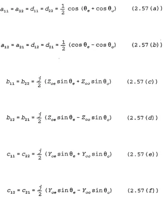
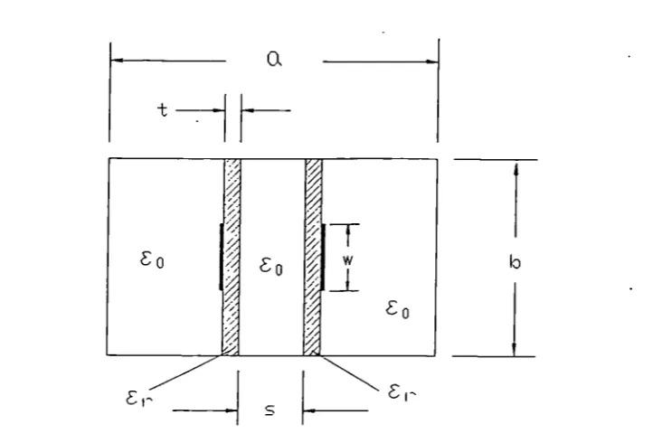
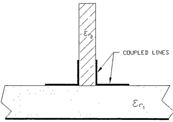
Coupled microstrip structures can be divided into three main types (a) edge-coupled (b) slot coupled (c) broadside coupled. Examples of these are indicated in figure 1.1 (a) through (c).
The forms of microstrip lines shown in figure 1.1 can support various modes depending on the degree of dielectric non-homogeneity when the structures are viewed in cross-section. Such modes may be divided into pure TEN, quasi-TEN and hybrid modes.
1.1 TEM MODE
The structures in Figs. 1.1 (d), 1.1 (j), 1.1 (k) will support a TEN mode if = 0, s = 0 and En = E; for the frequency range
0 ^ f ^ . An additional condition for a pure TEM mode to propagate is that one of the two conductors must have a finite dimension. Er is relative dielectric constant, an isotropic scalar
quantity and E 0 permittivity of free space.
12E0
Er1 h
Er,
Er,
177
T7
iri
rri
(a)
(b) (C)M S
E0
ii 2 0 2E
Er,
Er,
Er,
rr7
rr7
T7
(d) (e)
(f)
1 2 3
•••E
-Er1
T7
(g)
1
E0
El0Er,
Er,
flirT
--
rTi7
Co
(h) (i)
1
E0
-L
£
Er1
T
2
E0
rr7
(j)
Er1
Co
£
1
2
Er1
ri7
(k)
1
______
Er1
2
Erj
(1)
Figure l.l(j-l): Microstrip configurations
(a) Symmetrical edge coupled pair
(b) Same as (a) with dielectric overlay
(C) Same as (a) with tuning septum
(d) Same as (a) with lid in close proximity
(e) Same as (b) with extra strip at floating potential (f) Asymmetrical edge coupled pair
(g) Multi-line edge coupled system
(h) Microstrip slot coupled same as (c) with s = 0 (i) Coupled micro line
(j) Broadside coupled suspended microstrip lines, a variation of 1.1 (a)
(k) Broadside coupled inverted microstrip lines, a variation of 1.1
(j)
Characteristic impedance Z 0 and phase velocity VP of the TEM line are given by
1 (1.1)
c{C5C5
C
(1.2)
-Cs
eff (1.3)
a
where c, Ca C5, Eeffe are speed of light in a vacuum, capacitance of the strip conductor per unit length in the absence of a dielectric, capacitance per unit length of the strip conductor in the presence of a dielectric and effective dielectric constant respectively. For the TEM line Eeff = E. and Z 0 , V are single valued
1.2 HYBRID MODES
Microstrip will in general not support a pure TEM mode due to the dielectric non-homogeneity associated with the structure. As proof of this consider figure 1.2 rl.2]
Figure 1.2 Microstrip Structure
If the dielectric above the structure is air, the tangential electric field E equality at any point, (x, H) at the interface between air and the substrate results in
(VXH)xls = Ez( VXH)xla (1.5)
where a and s refer to air and substrate respectively.
VxH (, t) = J+ (.r, t)
andD(F, t) = €€ 0E(r, t)
Expanding(1.5)
ôy
wherei , j, k
are unit vectors in the x, y, z directions respectively. Applying (1.5) and taking into account the continuity of the normal component of displacement at the dielectric interface we arrive at
oH OH.. OH
(1.6) y
From (1.6), since H 0 and E r ]. must be non-zero. Similarly it can be proven that E * 0 by using Maxwell's equation
VxE(?,t) =--F,t)
addition to the total tangential current density J along the Z direction. Due to J the total conductor current I is no longer uniquely defined and due to E the voltage U = 5 E. ds is now path dependent. Therefore characteristic impedance u/I is multivalued and frequency dependent, as will be shown later. J although small compared with cannot be neglected if the complete dispersive nature of microstrip is to be accounted for and plays a particularly important role in characteristic impedance dispersion.
The fundamental mode behaviour can be predicted by taking into account the fact that an arbitrary electromagnetic field can be represented by a combination of TE and TM fields. A rigorous full wave analysis of the characteristic impedance and propagation constant is achieved by using the charge/current formulation [1.4] which follows:
Consider figure 1.2 where open microstrip is assumed with p.r = Er * 1, conducting strip thickness t = O, total charge on the upper
and lower surface of the conducting strip = p, and phase factor is exp j (t - yz). By applying the charge continuity condition
oJt + oJ = -op
ox
Oz ot8T
where is angular frequency and y is the propagation constant.
Bhat and Koul [1.4] has shown that the fundamental mode charge functions
f 2 (x),
g(x) associated with can in general be approximately represented byf(x)
1w2 -x2
g(x) =x () -x2
Figure 1.3 is a graphical representation of the fundamental mode and J based on [1.4]. The known charge singularities at the edges of the strip related to J is demonstrated.
0
2 2
Longitudinal Current Distribution on Nicrostrip, f(x) [1.4]
g1(x)
y
-w/2 0 w/2
w/2 w/2
C oj=f
j(yJ-op)dx=o
J -w/2 J -w/2
(1.9(a))
Then yJ=(.)Q (1.9(b)
where J,Q are total current density and total charge per unit length of the conducting strip and
Jdx (1.9(c))
o-f
dx (1.9(d))For the open structure in figure 1.2 J, can be determined by considering the radiation energy associated with strip current source J.
Under these conditions the following field equations (Maxwell's equations) can be written, where time dependence jwt is assumed and a perfect dielectric is assumed.
2A
8x 2 ôy2
(1.11(b))
VxH=j €E+J (1.10(b))
In a homogenous medium (in this case air) V . B = o 1.10(c))
and since any divergenceless vector is the curl of another vector.
B=VxA (1.10(d))
where A is defined as the electric vector potential. Substituting (1.10(d)) into (1.10(a)) results in
Vx(E+jA) =0 (1.10(e))
and since any curl free vector is the gradient of a scalar
Er -jA-V4 (1.10(f))
where is defined as the electric scalar potential then
82
ô+(K2_y2) =Q oy2
(1.11(a))
(J)./LQ
As shown in [1.5] A and can be expressed as functions of J, and p as follows:
= 2ice f Ge (x-x")
(XI') dx' (1.12 (a))
0 2
'1
A =a f i Gh x-x' J(x') dx "X 2ir
i
1 r
2ir€ j...W 0 j X M(x-x) (x') dx' (1.12(b))
Ay = 0, (1.12(c))
since the zero thickness strip ensures that there are no y directed currents.
w
A = f2
Gh (x-x') J (x') chc'
Z 2ic
l
f2 M(x-x') p5 (x') dx" (1.12(d))
w 2itc --2
where Ge (x-x'), Gh (x-x'), M (x-x') are Green's functions associated with unit charge at point (x') and given by:
1
K1 + €rK0 coth (K1H)
(1.13(f))
=Gh (a) -_____1(2 (1.13 (g)
M(x) =2f M(a) cos(ax)da (1.13(b))
Ge (x) = 2
f
ö
8 (a) cos (ax) da (1.13 (c))'h ,1f(a) , G (a)
represent Fourier transforms and are given by
Gh(cL) =
1
(1.13(d)) + i coth (K1 H)
zPr1) K2 =
rKoi coth(x 1 H) (CrK0+Ki tanh(K1H) )x0 (1.13(e))
K1 /a2 +y2 -C JL K2 (1.13(i))
Since the Green's functions must satisfy the boundary and interface conditions of the configuration under consideration these functions would be modified accordingly for closed microstrip.
From (1.10 (e)) and (1.12 (a))
E =j
A---V
= -J±2.
f
Gh (x-x') J (x l') dx' 2ir i(1.14(a))
- 1 I2 !:Ge (x-x') +M(x-x')
I r (x') dx' 2irc0
2
E5 = -jA5 + iYcI'
O
(2G (x-x')J5(x')dx' 2
1
+ Jy . +M(x-x')] p5(x')dx'
(1.14(b))
By applying the boundary conditions E = 0, E = 0 on the conducting strip and applying condition (1.8) ie. J (± w/2) = 0 Ps and J can be found.
parameter of interest is the characteristic impedance.
Characteristic impedance can be expressed by three different relations:
(a) Voltage - Current
(I V/I D
(b) Power - Current (2P/II*) (c) Voltage - Power (VV* , 2 P)All the definitions give different values. Definitions (a) and (C)
give an infinite number of values.
In this analysis the characteristic impedance Z 0 is defined as the ratio of the total electromagnetic power P flowing along the conducting strip to the square of the total longitudinal current
[1.5].
ie. Z 0 = 2P (1.15) where P is total average 11*
power in the z direction
P=-1ExHdS
2J
(1.16)
Applying equation (1.10) in (1.16) it can be shown [1.8] that P= P 11 + P 22 + P 12 (1.17)
P11
=-
ff
Z11 (x-x") . [J2 (x") J2* (x) +J (x') (x) I dx'dx (1.18(a))22
=-ffz
22(x-x') (-!p(x")
(p 5* (x))dx"dx (1.18(b))/ (I)
p
12
=ffz
12(x-x")
J (x) (—p *(x)) dx"dx (1.18(c))Z
11 (x-x'),
Z22 (x-x')
and Z12 (x-x')
are defined as distributed mutual impedances between points x and x' and the doubleintegration is over the strip ie. -wtow
2
Z11 (x-x") , Z22 (x-x') , Z 2 (x-x")
are given by
Z11 (x) =2f Z11 (a) cos (ax)da (1.19(a))
Z22 (x) =2
f
Z2 2 (a) cos (ax) da (1.19 (b) )(a) =-- • _!a_ Gh(a) (1.20(a))
2 2iiôy
Z22 (a) _(')(Y)2 1 -_ [(a)+I(a)] (1.20(b))
2 Co 2it€0 ôy
Z]2 () = j [a (a) +1(a)] (1.20(c))
Co 4icc0
Letting
p11 =Z11 II*,P22 = -Z22 II*,P12 = -Z12 II*thenZ0 = Z11 +Z22 +Z12 (1.21)
Therefore the dispersive characteristic impedance includes three terms, of these, as shown in [1.5], Z 11 , Z 22 are the most heavily frequency dependent. This frequency dependence increases as w/H decreases. The term is the TEM mode characteristic impedance.
1.3 QUASI-TEM MODE (Quasi-Static Analysis)
The Quasi-TEM mode is a special case of the hybrid modes where
ET > > EL and H1 > > HL where E1, HT, EL, HL are transverse electric and magnetic and longitudinal electric and magnetic fields respectively. The accuracy of these assumptions increases as frequency decreases. In addition Eaves and Bolle [1.7] has shown that if the radiating modes are not considered then microstrip propagation can be considered to be approximately TEM. This approximation approaches the exact condition at as E r -. or E0 or at frequencies where the dimensions of the structure represents a very small fraction of guide wavelength. Under any of these conditions the Quasi-TEM assumption can be made and quasi-static analysis techniques used. The approximation becomes increasingly inaccurate as frequency is increased.
Therefore instead of solving the time dependent wave equation
ô2 =0 ot2
which is what is required for the full wave analysis, Poisson's equation
or Laplace's equation
= 0
When
p =0
are solved for the Quasi-TEN case.
E,4
are electric field and scalar potential functions respectively.
The propagation constant has to be determined in the full wave
analysis, whereas in the quasi-TEN analysis the emphasis is on
determining the static capacitance, from which the characteristic
impedance is determined using equation (1.1). Ca and C in (1.1) are obtained by considering
Cr =E (1.22)
where r= a,s and V0 is the known potential of the strip with respect to ground.
where Pr(X') is the unknown charge distribution on the conducting strip which has to be determined. The core problem in quasi-static analysis is therefore the determination or accurate definition of
p 1 (x'). Using Green's function potential allows the transformation from a differential equation in to an integral equation where the unknown is the change density Pr Considering figure 1.2 the scalar potential at a given point (x,y) is given by
4 (x,y)
= I pr(X') Gr (x—x",y—H) thc" (1.24)
J-where G1(x-x',y-H) is the Green's function associated with a unit charge at x=x', The Green's function by definition satisfies Poisson' s equation
V2 G(x , y/x0i y0 )=!ô(xx0 ) .8 (y-y0 ) (1.25)
G(x,y/x0y0 ) in addition must satisfy the boundary conditions of the system. The Green's function can also be found by applying Laplace 's equation
(1.26)
where . is a tensor which reduces to
for an isotropic dielectric.
Equation (1.24) can be rewritten
w
= (x") Gr (x-x') dx" bc"I^ -, L'd (1.28) i
Equation (1.28) is applied to a coupled line configuration with strip spacing 'S' by applying voltages + V01 + V0 and + V01 - V0 to
the two conducting strips to represent the even and odd mode conditions.
The double strip coupled configuration can then be reduced to single strip conditions by taking advantage of the symmetry axis at x = o. The applicable boundary conditions then include a magnetic wall at x = o for the even mode (Neuman conditions) and electric wall at x=o for the odd mode (Derichiet's conditions) in addition to the other physical boundary conditions.
The even and odd mode characteristic impedances are from (1.1) 1
z0 (e/o) = ___________________
CVCa ( e / o ) C(e/o)
- +w
and Q
r (e/0 ) = Cr (e/o) v0 =c/of2 P r (e/o) (x')dx' (1.30)2
(e/o) designates even or odd mode. When V 0 = 1 and S is the spacing between the two conducting strips Pr (elo) is found from
(1.28) with V 0 = 1 and appropriate limits of integration.
I i-W
ie.1
=f
2 p(e/o) (x') Gr (e/0) (x-x")dx'
(1.31)
2where for the even and odd modes
Gj=Gr (XXI') +Gr (x+x'+S) (1.32)
Gj Gr (x-x') Gr (x+x"+S) (1.33)
reflecting the charge sources on each strip.
Once G 1 is known the problem is reduced to determining Pr(X) and
ultimately Cr• Several numerical methods exist for determining
Pr( X)t Cr, among these are:
1.4 METHOD OF MOMENTS
The method of moments [1.7) can be used to find the total charge
per unit length and thus characteristic impedance and effective
dielectric constant of two coupled microstrip lines in the
following manner. The unknown charge function Pr(X) on the strip
can be expressed as a linear combination of known basis functions
f(x)
such thatp(x) = a,,e f(x) 1.34(a)
p(x) = a,' f(x) 1.34(b)
where the a are unknown weighting constants which are to be
determined and n = 1, 2, 3----N
The superscript 'o' and 'e' refer to odd and even modes.
In order to achieve accurate solutions for Pr(X) with a low value
of N, the basis functions must be chosen to closely reflect the
physical conditions. For example the basis functions should
ideally display a singularly at the edges of the strips. They
Substituting (1.34) into (1.31) we get
l= a f32G(x_x')f(xI) dx' 1.35(a)
N
1= a' f 'G? (x-x) f (x') dx' 1.35(b) fl1 2
The inner product of (1.35) is then taken with another set of generally different known basis functions g(x), in = 1,2,----N to get
N S
<1,g(X)> == a. <g(x),
f
Ge (x-x')f(x')dx'> (136(a))fll 2
N
<1,g(x) > = a' . < g(x) , G° (x-x") f(x')dx'> 1.36(b)
fll 2
the inner product being defined as
<g(x),f(x) >=fz g(x)f(x) dx (1.37) 2
(1.38) (1.39)
(1.42(a))
Equation (1.36) is a set of linear equations of size N X N and can be expressed in Matrix form
[em] = [gmn] [ar]
ie. the a are given by [a n ] = [gmn] 1
[em] where g, = <g(x), 2 G (x-x') f (x') dx'>
2
(1.40)
1 .+w
and g = <g(x), 2 G° (x-x')f (x') dx'> 2
(1.41)
Substituting (1.40), (1.41) into (1.23) we get
N
a e 1'' (x) dx=C1,e
Js
n = 1 i
N
= af-'f1 (x) dx= CE
n = 1 2
(1.42(b))
for V equals unity.
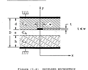
1.5 THE VARIATIONAL METHOD
y
d,E
______________ -
Ut
t
<wDs Era '.• ____
$ :: N N N
x
Figure (1.4) SHIELDED MICROSTRIP
So far open microstrip with t-. O has been considered, figure 1.4 shows, a microstrip structure with lid and a layered dielectric medium Erii E r2r Er3 In this case o * t << w. When s=o, E = 1 we
have regular microstrip.
The variational method of determining distributed capacitance Cr
based on the approach given in [1.11] begins with Poisson's equation in two dimensions linking the scalar potential (x,y) and the charge density function p(x,y)
1
V4(x,y) =---p(x,y) (1.42)
[image:34.595.87.448.95.382.2]where p(x,y) is represented by the Dirac delta function ie.
p (x,y) =ô(y-h-s-p)f (x) (1.43)
The spacing p between the strip and dielectric being introduced to equalize the number of variable and equations later [1.11]. One of the space variables in (1.42) is eliminated by taking the Fourier transform of all functions. ie .
ie. 1(13)
=1:1(x)
ejPJcdx (1.44)where f (3) denotes the Fourier transform with variable 3. Taking the inverse transform of (1.44) we get
f(x)
f
(13) e i d13 (1.45)Therefore (1.42) becomes
dy
p2
(ply) =0, (y^h+s+p) (1.46)
The general solution of (1.46) is of the form
2 (,y) = Bexp (ny)
+cexp (-3y)
(1.47(b))f) 3 ( p , y) Dsinh f3 (D-y) (1.47(c))
where A, B, C, D are constants to be solved. The ,
terms are expressed as hyperbolic functions to emphasize the fact that (J3,O), (f3,D) = 0 on the ground planes. When D -.
takes the form D exp (-f3 y). The general boundary conditions for the structure are then established in the Fourier transform domain
ie. i (f3 , O ) = 0 (1.48 (a))
(f3 , D ) = 0 (1.48 (b))
(3,h) = 2 (3,h) (1.48 (c))
r1 ( 1 (13 , h )) r2 (2 (3,h)) (1 . 48 (d))
2 (13 ,h + s) =& (131hs) (.148(e))
_d
r2 (2(1L h+S) - -- ( (3,h+s) (1 . 48 (f)
is associated with the air spacing p.
(13,h+s+p)) = r3 - (3(13,h^s+p)) (1.48(h))
in the charge free region.
where €r 1 , €r 2 , 1, €r3 are the relative dielectric constants of the layers and
1 '2 (13,y) , '0(1Ly) (tLy)
are Fourier transforms of the potential functions in each dielectric layer. By substituting (1.48) into (1.47) the solution
'(13,h+s)=_-1(P)(13) (1.49)
is achieved [1.11] where
( 13) =
[
Er
icoth
(113th) +E r2CO th (Ipis)] ^[113I{EriCOth(I13th) ) [€r3COth(IPId)
+ Er2 coth (I131s) +E 2 r2 r3C0t11 (1131s) I } II
The variational expression of Cr is then taken
Cr Q2fJ
(1.50)
(1.51)
Rather than taking the inverse transform of (1.49) we use the integral form of Parseval's equation [1.12] which is generally
(x) g(x)
dx=-Lff
(k) (k) dkto get
1= 1
f
f((,h+s)d
(1.51(a))
Cr 2itQ4
for t = o
If the thickness of the strip is taken to be t * 0 1 f[y()]2()
fi()
d
Cr itQ2€ 0
where
1^sinh(IId-IIt) }
(151(b))
sinh (I3Id)
Cr is then evaluated by choosing an 1(x) trial function which closely matches the physical charge conditions and taking
The capacitance calculated by this method is lower bound ie. it is always less than the actual value, therefore one criteria of choosing
f(x)
is to maximise Cr• Although this method provides a fairly accurate value of Cri generally, the trial functionf(x)
may not always be reliable depending on the configuration, therefore an upper bound of Cr should be determined to contain the margin of error. Araki and Naito [1.12] have presented a method for determining the upper bound of Cr in terms of a potential trial function V(x) at the interface containing the strip, rather than a charge function.This method also uses the variational technique in Fourier Transform domain.
The variational expression is then
=.2 --.
f
I(p)PIpI.
(1 4Er COth(P)
H) d (1.52) r 2it V2-1.6 THE SPECTRAL DOMAIN APPROACH
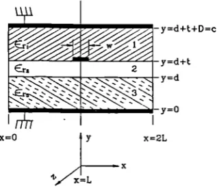
static and frequency dependent parameters of planar circuits. The main difference between the spectral domain approach and other moments methods is the application of Gellerkin's method in the transform domain ie. the transform of the set of expansion basis functions are the same as the transforms of the set of testing functions. Both full wave and quasi-static analysis are possible with this method by recognising that the partial differential equation considered in the approach for full wave analysis is the wave equation, and that for static analysis Laplace or Poisson's equation is considered.
The spectral domain approach is well suited for open or closed structures including multidielectric interfaces such as overlay couplers with conductors at several of these interfaces. In general the method has been applied under the following conditions:
(1) The conductors are assumed to have ideal conductivity o (2) Infinitesimal thickness t
(3) No discontinuities parallel to the dielectric interface (4) Lossless dielectrics
y=d+t+D=c
y=d
y=o
x =ZL
x=O y
method is used later in this thesis to analyze several complex microstrip coupled structures.
Figure (1.5) Shielded Microstrip Cross-Section
Consider figure 1.5 which has dielectric regions 1, 2, 3 with scalar effective dielectric constant E 11 , E r2 i E r3 and interfaces at y = d and y=d+t. Both the strip of width w and the walls at y=O and y = d + t + D = C are assumed to be perfect conductors.
To demonstrate the general spectral domain approach to the solution of microstrip structures the approach of Bhat and Koul [1.4] is
followed by defining the Hertz potential functions
4e(x
y,
z) and4Y(x,y,
z)as follows:
[image:41.595.199.358.138.276.2]x= (1.53(a))
- - ÔD
VxH=
-8t (1.53(b))
vi5=o (1.53(c))
(1.53(d))
•= —op (1.53(e))
(1.53(d)) implies, as stated earlier, that
(1.54)
where Ae is the electric vector potential. From (1.53(a)) and (1.54)
Vx(E+ OAè = (1.55)
as proven in (1.10(e)) which implies (1.10(f)) that
E=_V e _ (1.56)
Ot
Substituting (1.54) and (1.56) into (1.53(b)) and using the identities
Vx(VxA) =V(V.A) -V2A
D=
B =
or
_Xe^ €
+v[(v.
e) +ol
(1.57)otj
ô t2
Using the Lorentz condition [1.4]
v . A e +E (1.58)
it
(1.57) becomes
Ae_E o20 (1.59)
D= VxA' (1.60)
Where Ah is magnetic vector potential substituting (1.60) into (1.53(b)) we get
Vxi+--
(VxA') 0ie.
Vx(H+_-A') ..Q
and by definition
ôt
(1.61)
3t
where is magnetic scalar potential. By substituting (1.60) and (1.61) into (1.53(a)) we get
-8t2 (V.A) +E
o1 0 (1.62)
VPA h - ___ ___
ot]
(1.63)
(1.62) becomes
V2Ah_E
(1.64)
ôt2
Setting
Ae=Eô7t (1.65(a))
and
h.1ô7Ch (1.65(b))
where
e, jh are Her tzian vector potentials
and combining (1.65(a)) with (1.58) we get
ot
=0
(1.66(a))
ie.
Using (1.66(b)) and (1.56) we arrive at
E=V(V.e) (1.67(a))
and using (1.54) and (1.65(a)) we get
(1.67(b))
Similarly using (1.65(b)) in (1.63) we get (1.68)
and using (1.68) with (1.65(b)) in (1.61) we get
17=-H=V(V.)
8t2
(1.69)
and using (1.68) with (1.65(b)) we get
15= -i.t€ - Vx (1.70)
if time dependence exp jwt is assumed and k2 = E then following
[1.4] from (1.67(a)), (1.67(b)), (1.70) and (1.69)
= (1.71(b))
= jLVx1Ih (1.71(c))
h.(V ) -k2 (1 . 71 (d)
where
7h
are electric and magnetic field quantities associated with the vector potentials
and
2 + k2 e = (1.72(a))
-2 h + k2 h = (1.72(b))
since
satisfy the general wave equation
52i
727;1_Elt 0
ôt2
where i = e,h
Bhat and Koul [3.4] express the Hertz scalar potential
e , h
in the following terms
= (x, y, z) for E waves (TM) (1.73(a))
h4h (x,y,z)for H waves (TE)
(1.73(b))
where a superposition of TE to Z and TM to Z modes are considered to represent the hybrid modes associated with the structure in
figure (1.5). Z is a unit vector in the Z direction.
e (x,y,z) h (x,y,z) are defined as Hertz scalar potential
functions.
Then the wave equations (1.72) can be rewritten
(1.75(d))
'c724h^k24h=o
(1.74(b))
and the set of equations (1.71) can be rewritten
e_ (VÔ
+k2)
ôz
(1.75(a))
e =jEVx4e
(1.75(b))
h..
-j&Vx4
(1.75)h.. (V-p---
+k2)
4hôz
Equation (1.75) proves that the transverse field components can be deduced from the longitudinal component.
Equation (1.75) is then expanded - - 8 2 4 e -ô24
_( 24,e +
Ee
=x
+y +ôxôz
ôyôz
8z2
)
(1.76 (a))_4,e 4y
H 9 =jco€ (x— (1.76(b))
_o4h _84h
h__JL(x_y) (1.76(c))
h-+z( ô2 +k2h) (1.76(d)) ôxôz ôyôz 8z2
The total and H field are given by the following
(1.77(a)) [1.4]
H= H e + (1.77(b)) [1.4]
Now referring to figure (1.5) and assuming that the structure supports a hybrid mode which can be represented as a superposition of TM to Z and TE to Z modes, then the electric and magnetic fields in the structure can be expressed as follows: where i = 1, 2, 3 refers to the different dielectric regions, from equations (1.76) and (1.77) and assuming that the relative permeability of all dielectrics is unity. Assume also that the z dependence is exp jJ3Z (ie. propagation in the (-Z) direction).
From (1.76(a))
o2
E (x,y, z) = (--- +k 2)4 (x,y,z) (1.78(a))
82
H 1 ( x , y , z ) = +k2)4 (x,y,z) (1.78(b))
From (1.76(a)) and (1.76(c))
82 e E 1 (x,y,z)
= ôxôz (x,y,z) jo4 (x,y,z)
(1.78(c))
From (1.76(b)) and (1.76(d))
84i7____
H 1 (x,y,z) =JE1 (x,y,z) + (x,y,z)
oy ôxöz
(1.78(d))
From (1.76(a)) and (1.76(c))
8 2 .
E (x,y,z)
= 8yôz (x,y,z) +jo-_- (x,y,z)
(1.78(e))
From ( 1. 76(b)) and ( 1.76(d))
647 d2 h
+ ____ H 1 (x,y, z) = —j€1 -i---- (x,y, z)
ôyôz (1.78(f))
The simultaneous TN to Z and TE to Z condition results in = 0,
E 1 = 0, therefore
('
72 +k 2)4=O
(1.79(b))
Equation (1.79) is Helmholtz's equation. Assuming
€1 = E 0 Ez1 = (1.80(a))
€2 = E0E12 (1.80(b))
€ 3 = E0€r3 (1.80(c))
and letting the fourier transforms of the potential functions be e,h (a,y) fLeh (x,y) exp (jczx) dx
-L (1.81)
where a 1, is the transform variable and a = (2n—l)ic
2L (1.82(a))
when e is even in x, is odd in x
a = 2nir
(1.82(b)) 2L
when 1e is odd in x and •h is even in x. For the present case
(1.82(a)). For two coupled lines where both odd and even mode exists we would use both (1.82(a)) and (1.82(b)).
Then taking the fourier transforms of equation (1.78) and taking into account the Z dependence we get
(a,y) = (k -. 2) (,y) (1.83(a))
(c,y) = (k_p2) (a,y) (1.83(b))
(c 1y) =-oI3 (c' ,y) _j .__ (,y) (1.83(c))
(1.83(d))
(c 1y) =iI3
-4
(c,y) -o& 0 a (,y)(1.83(e))
(a,,y +j4 (a,y)
(1.83(f)
and
(d2 2
from (1.79), where
(1.85)
Equations (1.84), (1.83(c)), (1.83(d)), (1.83(e)), (1.83(f)) are proven by taking the inverse transforms.
We then establish solutions for (1.84) in the different regions i.
Taking into account the boundary conditions at y = 0, y = c the general solutions of (1.84) are.
IN REGION 1
f(c,y)
=A easinhy 1 (c-y) (1.86(a))(c,y) =A
h
(a
n)
coshy 1 (c-y) (1.86(b))IN REGION 2
y)
= e (a r ) sinh Y2 (y-d) + Ce
(a n ) cosh Y2 (y-d) (1.87(a))(,v)
= B"(a)
coshy 2 (y-d)+ch
(a fl ) sinhy 2 (y-d) (1.87(b))IN REGION 3'
4(a,y) =Dh(cc)coshy3y (1.88(b))
where Ae/h , Be/h , Ce/I , De/h are unknown constants which are to be determined.
Using (1.86), (1.87) and (1.88) in (1.83) results in the following set of equations.
= _3AeSjflhy1 (c-y) +jy1osinh 1 (c-y) (1.89 (a))
E 2 = - cP[B 9sinhy2 (y-d) + C9 coshy2 (y-d)]
(1.89(b))
_j i0y 2 [Bh S±nhy2 (y-d) + Cl2 coshy2 (y-d)]
= aPD sinhyy- jcüp.0y 3 D 1 sinhy3y (1.89(c))
E1=_j3y1AeCOShy1 (c-y) _caA hcoshy (c-y) (1.89(d))
v2
iP
Y2[B ecosh Y2 (y-d) + C'sinhy2 (y-d)](1.89(f)) _t1ii 0a[B h coshy2 (y-d) + C h sinhy2 (y-d)]
Ezi= (k_p 2 ) Ae sinhy1 (c-y)
(1.89 (h)
E32 =(k_p 2 ) [esinhy2 (y-d) ^C e coshy 2 (y-d)]
E 3 = (k_p 2 )D e S jflhy 3 y (1.89(i))
= _jo E1 A e y 1 cosh (c-y) - a I3A h coshy i (c-y) (1.89(j))
= j(a)E 2 y 2[B 8 coshy 2 (y-d) + c e sinh (y-d)]
(1.89(k)) -aP{B"coshy 2 (y-d) +Chsinhy2 (y-d)]
'x3 = coshy3yj - a D'cOShy3y (1.89(1))
sinhy 1 (c-y) - jy 1 sinh y 1 (c-y) (1.89(m))
= 2 a[B e sinhy 2 (y-d) + C 9 coshy 2 (y-d)]
(1.89(n))
+jf3y2[Bhsinhy2 (y-d) +C'coshy 2 (y-d)]
if= (k_p2) A h coshy 1 (c—y) (1.89(p))
'z2 (k_p2) [Bh COShy2 (y— d) +C h sinhy 2 (y — d)} (1.89(q))
''z3 (k_ 2 ) DhCOShY3Y (1.89(r))
In order to solve for the unknowns
A', B
e/h , Ce/I', De/h the following boundary conditions are applied at y = d + t.EX1 Ex2 for all x
E 1 = E2.
for
all xon the strip
- 2
w = 0, x>_
2
H22 H21 - J -- ' ^x^- on the strip 2 2
= 0 Ixt>-'
2
(Note: J (x ) = J(x) in section 1.3). at y = d
E2-Ex3 for all x
Ez2 - Ez3 for all x
H 2 =H 3 for all x(no current on the dielectric interface)
H 2 =H 3 for all x(no current on the dielectric interface)
After the Ae/h, Be/h, Ce/h , De/h are found, finally the general coupled equations
(ad^t) =2 (a)J(a)
+2(a,)
J(cc) (1.90(a))E(cd + t) =2(a)J(a) + ( a ,P)J (1.90(b))
are obtained [1.9] where
2zz' 2zx' 2xz' 2xx
it is done in section (4.2) for the quasi-TEM case, instead we repeat the analysis in [1.9] for completeness.
In (1.90) the
J are unknowns
can be eliminated by applying Gellerkin's method in the spectral domain in conjunction with Parseval's theorem.
To solve we start by defining the inner product [1.4]
< (an) , j (an) > => (an) 4(an) (1.91)
and Parseval's Theorem which states for figure (1.5)
f 1 (x) 2
(x) dx=--
(an) (an)then expand
I J(a)
= L a, J1 m=1. . .N (1.92(a)) !fl 1
rn=l. . .M (1.92(b))
where am, bm are unknowns.
The inner product is then taken with another set of testing function zk' for different values of k and Q where, k =
= 1,---M. [1.9]
Applying Parseval's theorem and the condition
E (x,d+t) = 0, Ex(x,d+t) =0
on the strip and the fact that zk' are zero outside the strip, then the following equations are obtained
I N M 1
+J Z bmJ,ijda=O,k=1,---N
m zm zk zx [ m=1
(1.93(a))
N M
52Ea j +j z bmJJda=Oi1=1i___M
m=1 m1
Equation (1.93) can be expressed in matrix form
N M
'ç-' ,.(1,l)
, "icm am +
k=l,2---N
(1.94(a))
m1 m=1
11,---M (1.94(b))
In order for (1.94) to have a non-trivial solution in a m, b m the determinant of the matrix must be zero.
and since in (1.94) [1.9]
K'
=f_: 2k (P) zm (x) dc
(1,2) r
K =j-,J 2(a,P) )cm da
K" f xi (a) (c,) zm (a) da
(2,2) r
Kim =_: (a) (a, 1) (a) da
f
a Z1 2zz JZ1 daf
zi 2zx 1 d1 ía1I
2 1 df
J 1 da [b1] =[a a J
the propagation constant p is found at a given frequency w by setting the determinant of (1.94) to zero to achieve a non-trivial solution. Once f3 is found, a m, b m are found by solving (1.94). The can now be found from 1.92 .. the fields can then be calculated.
Characteristic impedance variation with frequency is found by taking the power/current definition as outlined in section 1.2
= 2P
,whereP=f ExH ° 11* is
in the Z-direction and I =
V
f
JdxREFERENCES
[1.1] Reinmut K. Hoffmann, "Handbook of Microwave Integrated
Circuits
Artech House Inc.
[1.2] K.C. Gupta, Ramesh Garg, I.J. Bahi, "Microstrip Lines and Slotlines"
Artech House Inc.
[1.3] R.E. Eaves JNR and D.M. Bolle, "Guided Waves in Limit Cases of Microstrip"
IEEE Microwave Theory and Techniques Volume MTT-18
April, 1970 Page 231 - 232
[1.4] Bharathi Bhat and Shiban Koul, " Analysis, Design and Applications of Fin Lines'
Artech House 1987 Page 130
[1.5] Masahiro Hashimoto, "A Rigorous Solution for Dispersive Micros trip"
IEEE Microwave Theory and Techniques
Volume NTT-33, No.11 November, 1985 Page 1131-1137 [1.6] Robert S. Collin, "Foundations of Microwave Engineering"
McGraw Hill: New York, 1966 Page 32
[1.7] N.G. Alexopoulos, "Integrated Circuit Structures on Anisotropic Substrates"
[1.8] Raymond Crampagne, Magid Ahmadpanah, Jean-Louis Guiraud, "A Simple Method of Determining the Green's Function for a Large Class of MIC Lines Having Multilayered Dielectric Structures"
IEEE Transactions on Microwave Theory and Techniques Volume MTT-26 No.2 February, 1978 Page 82 - 87 [1.9] Tatsu Itoh, "Numerical Techniques for Microwave and
Millimetre Wave Passive Structures"
John Wiley and Sons New York, 1988
[1.10] Nirod K. Das and David M. Pozar, "A Generalised Spectral Domain Green's Function for Multilayer Dielectric Substrates with Application to Multilayer Transmission Lines"
IEEE Transactions on Microwave Theory and Techniques
Volume MTT-35 No. 3 March, 1987
[1.11] Eikichi Yamashita, "Variational Method for the Analysis of Microstrip Like Transmission Lines"
Planar Transmission Line Structures, Edited by T. Itoh
IEEE Press 1987 Page 3 - 9
[1.12] Roger F. Harrington, "Time Harmonic Electromagnetic Fields"
McGraw Hill: New York, 1961 Page 182
[1.13] Kiyomichi Araki and Yoshiyuki Naito, "Upper Bound Calculations on Capacitance of Microstrip Lines Using Variational Method and Spectral Domain Approach"
[1.14] Jeffrey B. Knorr and Ahmet Tefekciglu, "Spectral Domain Calculation of Microstrip Characteristic Impedance" Planar Transmission Line Structures, Edited by T.Itoh,
IEEE Press 1987 Page 74 - 77
[1.15] Rolf H. Jansen, "The Spectral Domain Approach for Microwave Integrated Circuits"
CHAPTER 2
APPLICATIONS OF COUPLED HICROSTRIP LINES
2.0 INTRODUCTION
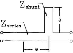
Coupled microstrip lines in anisotropic substrate configurations are used extensively in microwave/millimetre wave circuits. The more popular functions are as directional couplers, filters, delay lines and interdigital capacitor [2.1]. Less exploited functions, so far are as high impedance low loss transmission lines [2.2] and as impedance transformers in matching circuits or as phase shifters. In the above applications coupling between the microstrip lines is a desired attribute, in other applications such high density multilayer thin film interconnects used in VLSIC, VHSIC and megabit memories [2.3] interconductor coupling is a nuisance whose importance cannot be ignored as frequency increases and therefore must be understood. In this chapter the coupler, phase shifter and impedance transformation functions will be considered.
2.1 MICROSTRIP COUPLER WITH EQUAL WIDTH LINES (SYMMETRICAL)
Substrate
H
Microstr p1 i ne
w-_-
S _ W
-(2.1(a))
Electric field lines - --- Magnetic field lines
--
---,_ - N
Even mode
(2.1(b))
- -- - - -
-Th(i (2.1(c))
figure 2.1(b), and 2.1(c); which indicate that in the even (unbalanced) mode the voltages on the strip are in phase ie. V 1 =
V2 whereas in the odd (balanced) mode they are 1800 out of phase ie. V2 = -V 1 . Superposition of odd and even modes describe propagation
in the structure. To examine the coupling behaviour of such strips consider figure 2.2 in which all four ports are of the structure are terminated by impedances Z 1 , Z 2 , Z 3 , Z4.
0 is the electrical length of the coupled section and voltages and currents are as shown. Z 00 , Zoe are odd and even mode impedances.
V:V3
oe' 00
Figure 2.2 Coupled Microstrip
ZctnO ZctnO ZcscO ZcscO
ZctnO ZctnO ZcscO ZcscO
[z) =—j
ZO (2.1)
ZcscO ZcscO ZctnO ZctnO
where
Z+= (Zoe+Z ' 00 / /2
Z.. = (Z0 Z00 ) /2
for the special case Z 1 = = = = Z 0 , it is shown that by superposition of odd and even mode voltage and currents the in put impedance of the coupled line section at port 1 is
= V1 + Vie
ifl T +T
10 ie
(2.2)
where o, e refer to odd and even modes then
z10
z - _____
1
zo + zio
z
+ le
z +za 1e
(2.3)
+ 1
Z o ^ Zie
Using the transmission line equation
-
zoo{ Z
o + j Z00
tan 01
-
Zoo+jZ0tanOj(2.4)
Zie - Zo + j Zoe
tan
01-
Z0+jZ0tan0]
(2.5)
and substituting 2.4, 2.5 into 2.3 it is found that if
i
Z0 = (z 0 . Z0) 2 (2.6)
then Z
i ri = Z 0ie. the coupler is matched. When condition (2.6) holds
then the scattering matrix of the coupler is
Io S12 o S141
S12 0 S14 0
[SH
0 (2.7)[514 0 S12 0]
where
S
=
jksinO
(2.8)Il-k2
(2.9)
S14 = _______________________
/1 -k 2 cosO + j sinO
k= Zoe/Zool
(2.10) Zoe/Zo + 1
where k is the voltage coupling coefficient. From (2.7), (2.8) and (2.9) the following coupler characteristics can be deduced (for the unique case of
zo = /-2;-z00
1. The device is a quadrature coupler.
2. Coupling is in the backward direction (S12)
3. The directivity is infinite
4. voltage coupling constant is dependent on the ratio Z061Z00.
There are three important additional constraints on the structure which leads to conditions 2 and 3.
They are as follows:
(a) The lines are symmetrical (b) The coupler is matched
(C) The phase velocities of the odd and even modes are assumed to be equal.
2.2 MICROSTRIP COUPLER WITH ASYNMETRIC LINES
When the lines in figure (2.2) are asymmetrical (ie. of different widths) Crystal [2.5] shows that infinite directivity is achieved
if
GaGb = AB -D 2 (2.11(a)) There are two conditions for impedance matching
Ga Gb =ABD2 (2.11(a)) and
Ga/Gb=A/B (2.11(b))
where Ga Gb are the terminating admittances of the two lines, which need not be real,
ya + ya 00 oe
(2.12(a)) 2
E=
Yobo+Yobe
(2.12(b)) 2
V a Va vb
D = 00 - - oe = 00 - (2.12(c))
2 2
where ya ya are admittances measured at port 1 for an infinite section of coupled line excited in the even and odd modes respectively, with voltage sources at ports 1 and 2.
yb yb
are corresponding even and odd mode admittances measured at port 2 with sources at ports 1 and 2. [2.5]k=D'I',/A"B' (2.13(a))
(A'\
Ga = , )(fA /B I_ D 2 ) (2.13(b))
Gb=()(A/BI_D2) (2.13(c))
and the theoretical limit of the impedance transformation ratio (between incident and coupled ports) for a given coupling value is given by
(2.13(d))
k 2 Gb Ga
The asymmetric coupler can be designed from a knowledge of the symmetric coupler of equal coupling by applying the fact that an asymmetrical coupler is mathematically equivalent to a symmetric coupler where the coupled line of the symmetric coupler has impedance transformers of turns ratio
1:7A
connected at both ends, (ie. ports 2 and 3). And Crystal [2.5] shows that the following equivalence is valid
A=A' (2.13(e))
N = B' / A1 (2.13 (f)
D = Dl'/N (2.13 (g)
A frequently encountered problem of microwave system design is the requirement for a transition from 50 to 75 ohms at the IF band. The requirement for a compact transition is presently met by using a resistive divider. The resistive divider approach reduces dynamic range of the system. It is proposed here to achieve a low loss compact transition from 50 to 75 ohms at NHz frequencies by using an asymmetric spiral coupler similar to the type shown in figure (2.11), with ground plane septum, to achieve the required value of k.
From equation (2.13(d)),
= 1.5
k2
ie. k = 0.81
and = 9 . 5
00
This ratio can be met by the ground plane septum method analyzed in chapter 4. The transformer design will be as follows: (1) for the selected substrate determine the line spacing and septum lengths which result in the required even to odd mode impedance ratio for symmetric lines (2) use equation (2.13) to determine the width of the coupled line in the asymmetric configuration.
2.3 MISMATCHED COUPLER
To address the case where the coupler is mismatched let the input impedance at port 1 be Z 1 ,< where x = '0' or 'e' and let Z 0 be the source/load characteristic impedance.
Then
and if
ak = = coupler impedance
k= ae - a0 = voltage coupling coefficient
+
k1 =/L— k2
then from [2.5]
(a-1) +k(c+1)
Slm = J sinO {
2 a k kl co50+js0[ k +1) +k(a-1)]
± (cc-1) -k(c+1)
2a
kk
lcosO+jsinO[(a.+l) -k(a.-l)]
(2.14(a))
where m = 1, 2 and the positive sign and negative signs in (2.14(a)) refers to S 11 and S 12 respectively.
Similarly
Slfl-o:kkl{
1
2akklcosO+jsinO{(a+1)+k(a_1)]
1
± }
2a k kl co sO +jsinO[(c4^i) —k(c4^1)]
(2.14(b))
where n = 3,4 and the plus sign refers to S 14 and the minus to S13.
when ak-i
(2.14) reduces to (2.7) the matched coupler case. 2.4 UNEVEN PHASE VELOCITY
So far equal even/odd mode phase velocities h However, due to the dielectric inhomogeneity structure even and odd mode phase velocities Vpei
re been assumed. the microstrip
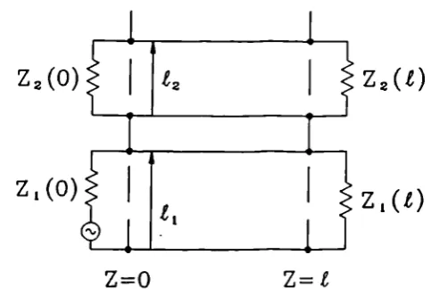
Z2(0)
Z1(0)
z2(t)
z1(t)
z=o z=t
Figure 2.3(a) Coupled Microstrip
L2 C2 L 2 C2
$T
Lm 'Cm
--Im
$ ___
C l Cl
--_ 1
_
Z=Z 1 Z=Z1 +dz
Figure 2.3(b) Equivalent Circuit
Krage and Haddad [2.7] using the notation in figure 2.3(b)), where L, C, (j = 1, 2) are equivalent self inductance and capacitance respectively per unit length of each strip j in the presence of the other line k (k = 1, 2) where j k and L m C m are mutual inductance and capacitance per unit length, respectively, indicates that the behaviour of the system can be described by the following equations
l+L ---+L -=o
(2.15(a))
[image:76.595.117.405.83.495.2] [image:76.595.154.396.92.258.2]6i +C -- =0
1 ôt m
ôe
—1+L
-02
ôz öt
ôi
=0 ot ôt
(2.15(b))
(2.15(c))
(2.15(d)) L = L — L L = L — L C = C -I-C C = C +
1 10 in' 2 20 in' 1 10 m' 2 20 m
Assuming that the lines are lossless and that the impedances of each line is not a function of distance, Z, along the line then the propagation constant
y = ±j 0 1±ö (2.16)
ie. four possible phase velocities if the medium is homogenous only one phase velocity is allowed and 6 o
and
where = _____
N
2 -I3lIG2kLkCo
1
1 2 2\ =
'2l
(1 — kr) (1—k)
(2.17)
(2.18)
I3I = /LJ C1 (1 = 1,2) (2.19)
Z2 (0) I
LINE 2
z2(t)
I +1
LINE 1 -a
z1(o) - z1(t)
[image:78.595.125.394.89.297.2]Z=0 z=t
Figure 2.4 Schematic for Coupled Wave Analysis
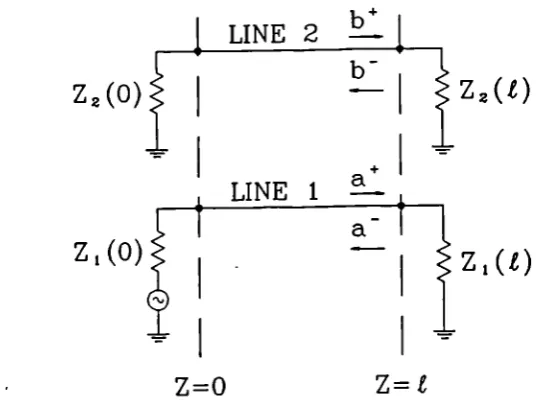
Considering figure 2.4 in which the modes on the line are represented by a+, a, b+, b with directions as shown.
For a homogenous medium ie. 8 = o and setting P = 2EMconditions) (ie. the symmetrical condition referred to in section 2.1) and matched terminations, then kL = = k or kL = (2.18)
and Krage and Haddad have shown that the reflected wave
a(o)
= (2.22)
a(o)
the transmitted wave
____ = (i-k2) (2.23)
the coupled wave
b(o) = jksinO
(2.24) a(o)
/(l-k2)
cosO+jsinOthe directivity related wave
= 0 (2.25) a+(o)
where
o = and C= l/v1jI
C
t and E are permeability and permittivity of the homogenous medium
respectively.
It is worthwhile to note that equation 2.24 is identical to (2.8).
Defining coupling
Eb(o) P
(1-Ip2(o)12)
(2.26)
Ia (0)12
Ib (Q) P (1 ....1p2()12 )
(2.27)
D=
N
(o) P (1 -lp2 (o) 2)where p1(Z) is voltage reflection coefficient of line i at a
position Z. Then using equations (2.20), (2.21), (2.22), (2.23), (2.24) and (2.25),
/ksinO
(2.28) - - k2 cos2 0
D=o (2.29)
For the non-homogenous dielectric case kL k. If in this case = P 2 and the ports are matched
then
PO=131V1-kLkC (2.30) from (2.15)
and
8 = (kL - k) / (1 - kL k) (2.31)
and following [2.6] defining
and
4
2=
[(1-
k
L) (1 + k)
(2.33)(2.34)
(2.35)
A =kL - kc (2.36)
then
and
c=lb(0)I (2.37)
a (°)
b(o) =
(kL
+
kc) {[2cos(6 1 -'-0 2 ) -2cos (01-02)] a4(o)^j[(1^42)sin(81+O2)+(2-41)Sifl(O1O2)]}
--[4 (i+44) -A2 ] cos (01+02) - [4 (1 4142) - A 2 ] cos (0 -02)
^iC [4 (4-)
+2
(42-41)] sin (0+6..,)-[4
(44)
-2A (412)] sin (0-O))b (Q)
D=Iand
b () = (2
(4'142) (cosO 2 -CoSO1 ) +j [2 (
4 1 sin0 2 42 sin01)
b (o)
-A ( 1 s1fl0 2 +42sin01)])
(2.39)
{(kL+kc){2
[cos(0 1 +0 2 ) -COS (0-0)]
+j [(41 +4:2) sin ( °1°2 ) + (4142) sin ( 0 1-0 2 ) ]}}
As is increased [2.61 power coupled to the b mode is decreased and power coupled to the b mode is increased which results in degraded directivity as well as co-directional behaviour if is increased sufficiently.
For optimum contra-directional microstrip coupler performance it is therefore necessary to find means of making A o ie. equalising V0
and Vpe Chapter 3 deals with techniques of achieving this condition.
2.5 COUPLER BANDWIDTH SENSITIVITY TO ZoelZoo
Ratio of power at port 2 of the coupler to input power at port 1 is
given by [2.11]
Where 0 is the electrical length of the coupler
C 2 = k forO =
-The value of 0 for which
R2 - =m
k2
is given by
om_sin-1[(mm'
(2.40(b))
- 1_mk2)
If fractional bandwidth BW is defined as
then since O = and
-f- = --
ICThen fractional bandwidth for a given m is
pw=l_ sin i (mmk (2.40(c))
ICL2 l_mk2)
Where fc is frequency at which m = 1.
Since
k=
1 + Z00/Z
bandwidth is maximised by minimising the ratio Zoo/Zoe•
Chapter 3 examines ways of achieving this.
2.6 COUPLED MICROSTRIP LINE PHASE SHIFTER
Referring to figure 2.2 if ports 2 and 4 are short circuited then the ABCD matrix of the structure becomes [2.5].
A= Yo&COtOe+YooCOtOo (2.41(a))
'oecosec 0 & -
cosec 00
2j
(2.41(b)) 8=
oe cosec 0e -
cosec
60c
'0 + 'oc2
Y00 Y00(cot O e cot 0 0
^cosec Oecosec 0)
=
2
cosec -
cosec
D=A (2.4:(d))
23
1 4
1:—i
Figure 2.5 Terminated Coupled Line Equivalent Circuit
From equation (2.41) when Z >> Z ie. Y << Y the ABCD matrixoe 00, oe 00 elements are approximately
A = D = -cos
B = -2jZ00sinO0
C =
-ie. the equivalent transmission matrix becomes I cos6 0 j2Z0sinO0l
° U
sinO0
L 0 _1][J
2Z00 cosO0
(2.42)
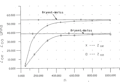
offers a simple technique for achieving in planar form the 1800 phase shift required for broadband push-pull amplifiers and balanced mixers. As part of this exercise a 90 degree section of coupled line terminated as mentioned above was used to replace the 270 degree section of a microstrip rat race. The circuit layout is shown in figure (2.5(a)). The circuit was realised on 0.025 inch thick Epsilon 10 (r = 10) with line spacing of 0.0017 inch and line width 0.016 inches in the coupled section, resulting in Zoe/Zoo
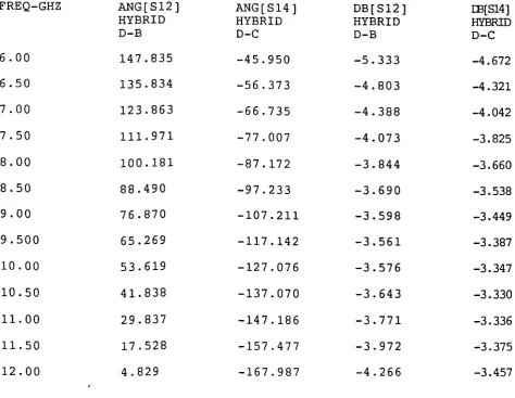
ratio of 2.7. Predicted data is shown in table (2.1). Figure
(2.5(b)) shows measured phase response of the path D to B versus D to C.
Measured data was as follows:
Frequency Band 7.5 to 10 GHz (28%
bandwidth)
Coupling DtoB 3 ± 0.2 dB
COUPLING D to C 3 ± 0.2 dB
COUPLING D to A 10 dB minimum
PHASE DIFFERENCE D to B vs. D to C 180° ± 10°
U E -w (/) E • 1-0 -I-, 0 >, -J LC w 5. -0) LL '-I
a: flJ(fl =
-w
ai- I
uj u _J o- rn •r
U)
-W - U) = C'J
a:w QLor- &) 00 ijJo
w C)
a:1i -ic
lii - -, • LI >< cr, U)
>( a lfl (.0
• >< -i c\i - z •r-•
•U)E a:
>z c w w
• >< - I- U) cr U) ' = U) ) C) LU C) =
LU
I-C) • •
Cu Ifl
The bandwidth over which (2.42) holds is dependent on the ratio Z oe/ Z oo = M as shown in section . (2.5). In section (2.8) we propose a broadband 1800 phase splitter in which very high Zc/Zoo ratio is achieved by the use of the tuning septum approach which is analyzed in chapter 4.
Touchstone(TN)-Configuration (100 1600 100 17405 0651 1000 1 3294)
FREQ-GHZ 6.00 6.50 7.00 7.50 8.00 8.50 9.00 9.500 10.00 10.50 11.00 11.50 12 .00 ANG{S12] HYBRID D-B 147.835 135.834 123.863 111.971 100. 181 88.490 76.870 65.269 53. 619 41. 838 29.837 17 .528 4.829
ANG [ S 14 1 HYBRID D-C -45.950 -56.373 -66 .735 -77 . 007 -87 . 172 -97 .233 -107.211 -117.142 -127.076 -137.070 -147 . 186 -157.477 -167.987
[image:88.595.51.526.276.643.2]<r\i;iJ In
pir'i a)
0•
woo
R)O
000
N.
N
I-(D
- fl
c
-ncnn
om
ZH
•
m
0,
0 0
(DQ)
00
(1) (D(DII
NN
0 V) (D0
V)
0
•
NJ
2.7 SELECTIVELY TERMINATED COUPLED MICROSTRIP
2.7.1 PORT 2 SHORT CIRCUITED PORT 3 OPEN CIRCUITED
Consider figure 2.2. If port 2 is short circuited and port 3 open circuited the equivalent circuit is shown in figure 2.7 [2.1O, in a non-homogenous configuration.
ZshuflU
[image:90.595.215.365.258.366.2]Zseries\
Figure 2.6 Equivalent Circuit Where
2 Z0eZ00 Zseries
(Z +Z ) oe 00 (2.43(a))
I 09 —z \200'
ZShuflt 2'Z +Z ) (2.43(b))
oe 00