Broadband Quasi-Yagi Antenna for WiFi and WiMax
Applications
Jean-Marie Floc’h, Ahmad El Sayed Ahmad
Unité Mixte de Recherche 6164 (UMR), Institut d’Electronique et de Télécommunications de Rennes (IETR), Rennes, France. Email: ahmad-khoder.el-sayed-ahmad@insa-rennes.fr
Received January 17th,2013; revised February 21st, 2013; accepted March 7th, 2013
Copyright © 2013 Jean-Marie Floc’h, Ahmad El Sayed Ahmad. This is an open access article distributed under the Creative Com-mons Attribution License, which permits unrestricted use, distribution, and reproduction in any medium, provided the original work is properly cited.
ABSTRACT
In this paper, we present a broadband quasi-Yagi antenna. Good impedance matching is obtained by using parasitic elements. The antenna has been designed and successfully measured. Experimental results show that the 10 dB return loss bandwidth of this antenna is 50% operating from 2.3 GHz to 3.8 GHz. We obtain very flat gain (around 5 dB) over the entire bandwidth. For the design and optimization of antennas, we use HFSS CAD software from ANSOFT.
Keywords: Printed Dipole Antenna; Quasi-Yagi Dipole Antenna; Broadband; Director; Reflector
1. Introduction
Nowadays, quasi-Yagi antenna is widely used in wireless communication for its high directivity, high radiation efficiency, low cost, low profile, as well as easy to fabri- cation [1,2]. However, the main disadvantage of these antennas is narrow bandwidth and the bandwidth com- monly achieves just 10%. To solve this problem, re- searchers have made great efforts to improve the band- width of Yagi antenna using many ways.
Several different techniques have been proposed in lit- erature, concerning the enhancement of impedance band- width in microstrip antennas, mostly by increasing the substrate thickness, by decreasing the substrate dielectric constant [3], and by alternative feeding methods (aper- ture coupled or proximity instead of direct contacting feed). Moreover, by increasing the width of the printed dipole antennas, the bandwidth of antenna increases [4]. By using triangular instead of rectangular dipole arms (bow-tie-configuration), the bandwidth can be further expanded to 37% as presented by Bailey [5]. Coplanar parasitic elements have been proposed by Deal et al. [6] in a quasi-Yagi configuration, yielding an impedance bandwidth of 48%. A similar Yagi-like double sided an- tenna [7], achieved a bandwidth of 37%. Stacked para- sitic elements (aperture attacked patches) are widely used for enhanced bandwidth, but their fabrication is relatively complicated and expensive. Additionally, a broad-band quasi-Yagi antenna achieving a measured 48% band-
width is presented for radar systems and millimeter-wave imaging arrays in [8]. We have presented few year ago in [9] a multi-band frequency printed dipole antenna with operation at 2.45, 5.8 and 10 GHz.
The paper is organized as follows: first, we present the design concept of the proposed printed dipole antenna with reflector (with minimal complexity design). In Sec- tion 3, a parasitic element is embedded to increase the bandwidth of antenna. Finally, the printed dipole antenna with a three parasitic elements is studied to enable the operation of wideband. The antennas have been designed and successfully measured.
2. Basic Antenna
The quasi-Yagi printed dipole antenna is composed of the dipole and reflector as shown in Figure 1. The two arms of the dipole are printed on each side of a CuClad substrate of thickness 0.8 mm and permittivity of 2.17 (to overcome the complicated feeding technique). We use a microstrip line combined with a bifilar printed line. The length of these arms and the distance between them and reflector are around quarter-wavelength (λ0/4). λ0 is the
wave-length in free space corresponding to resonant fre-quency around 2.45 GHz.
direction, it performs as a director (θ = 180˚).
The advantage of this structure is to increase the gain of the printed dipole and to decrease the backside radia- tion. The Figure 2 shows the realized printed dipole an- tenna with reflector.
The simulated reflection coefficient evaluation is shown in Figure 3. The printed dipole antenna is matched to −29 dB in simulation around the operating frequency. The measurements were achieved in the laboratory anechoic chamber and have been compared to simulation. The return loss of the tested antenna is pre- sented in Figure 4. The level of measured S11 is lower
than −10 dB over the frequency bandwidth [2.3 GHz - 2.7 GHz].
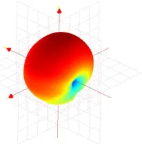
We present the radiation pattern in 3D at 2.45 GHz obtained in simulation and measurement (Figures 5 and 6). We note a good comparison between simulation and measurement. The measured gain in 0˚ and 180˚ direc- tion is respectively 5 dB and –8 dB at 2.45 GHz. The difference between the simulated realized gain and the measured realized gain is around 0.5 dB. The measure- ment accuracy of the anechoic chamber (±0.5 dB) can be responsible for this variation.
3. Antenna with Parasitic Elements
3.1. Antenna with One Parasitic Element
[image:2.595.311.536.83.243.2]The addition of one parasitic close to the simple printed dipole creates a second resonance frequency (Figure7). The resonant band is obtained through coupling between
Figure 1. Geometry of the printed dipole antenna with re- flector.
[image:2.595.311.536.290.454.2]Figure 2. Photo of the printed dipole antenna with reflector.
Figure 3. Simulated reflection coefficient of the simple printed dipole.
S11
[image:2.595.87.258.457.555.2]S11
Figure 4. Measured reflection coefficient of the simple printed dipole.
Figure 5. Simulated 3D radiation pattern of the dipole an-tenna with reflector.
the dipole arms and the parasitic strip. This frequency is determined by the length of the parasitic around λ0/2. We
[image:2.595.312.536.496.649.2] [image:2.595.91.256.593.719.2]The distance between the dipole arms and the parasitic dipole is very short because the coupling between them is capacitive. The realized antenna is shown in Figure8.
The simulated and measured S11 of this antenna is
plotted in Figure9. The addition of one parasitic close to the simple printed dipole permits to increase the band- width of the antenna. We note a good similarity between measurement and simulation. We obtain with this an- tenna around 1 GHz bandwidth for a S11 < −10 dB (2.3
GHz - 3.3 GHz).
[image:3.595.310.540.86.220.2]We present the measured radiation pattern at 2.45 and 3 GHz. The maximum value of measured realized gain of the antenna with one parasitic is 5 dB in θ = 0˚ (Figure 10). In the Figure 11, we can see the measured maximum gain versus frequency. We observe a flat gain over the fre- quency band 2.3 GHz to 3.3 GHz at the value around 5 dB. The efficiency of this antenna is greater than 75% over the frequency band.
[image:3.595.308.538.256.698.2]Figure 6. Measured 3D radiation pattern of the dipole an- tenna with reflector.
Figure 7. Geometry of the quasi-Yagi antenna with one parasitic.
Figure 8. Photo of the quasi-Yagi antenna with one para- sitic.
Figure 9. Simulated and measured return loss of the an- tenna.
(a)
[image:3.595.120.223.313.417.2](b)
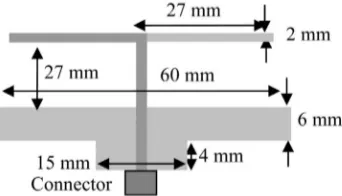
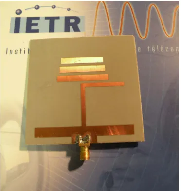
[image:3.595.96.250.457.544.2] [image:3.595.106.239.581.710.2]3.2. Antenna with Three Parasitic Elements In order to increase more the antenna bandwidth (for WiFi and WiMax applications), we have added three parasitic elements on the bottom side of the substrate where one dipole arm; the reflector and the ground plane were printed (Figure12). Each parasitic element should be shorter than the length of the two dipole-arms for create a resonances greater than the resonance of dipole antenna. Three parasitic elements are sufficient to cover the WiFi and WiMax bands. The antenna is designed using the same size of the prototype described in 3.1, with the new parameters of the three parasitic elements. The lengths of these parasitic elements are: 32 mm, 29 mm and 27 mm. The width is 4 mm. The distance between them is 2 mm. The tested antenna is shown in Figure13.
The broadband printed quasi-Yagi antenna is matched in simulation over the operating frequency bandwidth. The return loss of the tested antenna is presented in Figure14. The level of measured S11 is lower than −10
dB over the operating frequency bandwidth (2.3 GHz - 3.8 GHz). We note a good similarity between measure- ment and simulation. We obtain a bandwidth of 1.5 GHz (around 50%).
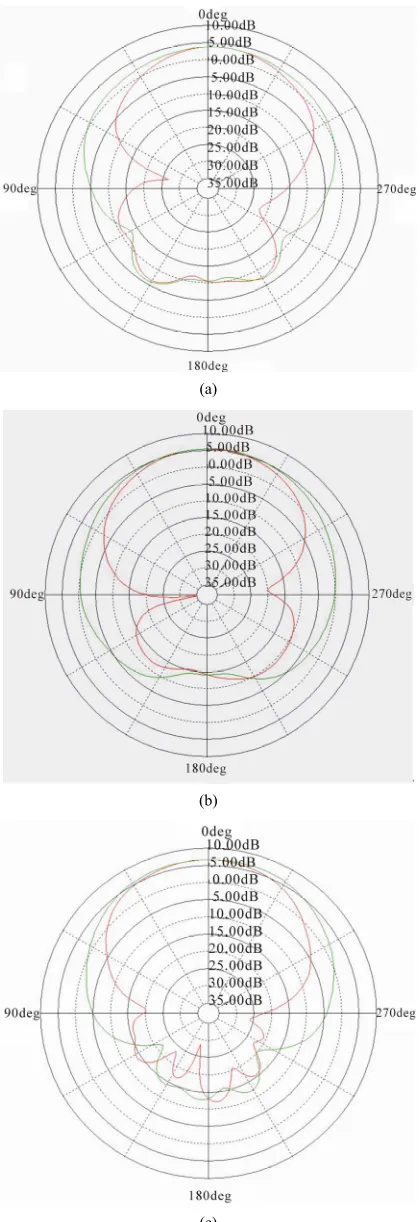
Figure 15 presents the measured radiation pattern at
2.2 GHz, 3 GHz and 3.8 GHz. We observe a very stable radiation pattern with less than −10 dB backside radia- tion versus the bore sight direction.
[image:4.595.331.517.84.280.2]In terms of levels (Figure16), the measured realized
[image:4.595.315.533.319.456.2]Figure 11. Measured gain versus frequency.
Figure 12. Geometry of the quasi-Yagi antenna with three parasitic elements.
Figure 13. Photo of the quasi-Yagi antenna with three parasitic elements.
Figure 14. Simulated and measured return loss of the antenna.
gain at θ = 0˚ is higher than 5 dB over the band [2.3 - 3.8] GHz. We can observe from the Figure 16 that the gain is flat over the frequency band 2.3 GHz to 3.8 GHz. The efficiency of this antenna is greater than 70% over the frequency band.
4. Conclusion
[image:4.595.70.279.360.719.2] [image:4.595.77.269.436.562.2] [image:4.595.79.264.597.707.2]Figure 16. Measured radiation results (realized Gain) ver-sus frequency of the broadband quasi-Yagi antenna.
impedance and gain bandwidths (50%). At the same time, this antenna possesses low profile and miniaturization characteristics. Furthermore, the wide beamwidth and high gain can promise the antenna to be widely applied in many communication systems.
(a)
REFERENCES
[1] G. R. DeJean, T. T. Thai, S. Nikolaou and M. M. Tentze- ris, “Design and Analysis of Microstrip Bi-Yagi and Quad-Yagi Antenna Arrays for WLAN Applications,”
IEEE Antennas and Wireless Propagation Letters, Vol. 6, 2007, pp. 244-248. doi:10.1109/LAWP.2007.893104 [2] O. Kramer, T. Djerafi and K. Wu, “Vertically Multi-
layer-Stacked Yagi Antenna with Single Ande Dual Po- larizations,” IEEE Transactions on Antenna and Propa- gation, Vol. 99, 2010, pp. 1022-1030.
[3] E. Levine, S. Shtrikman and D. Treves, “Double-Sided Printed Arrays with Large Bandwidth,” IEEE Proceed- ings of Microwaves, Antennas and Propagation, Vol. 135, No. 1, 1988, pp. 54-59. doi:10.1049/ip-h-2.1988.0010
(b)
[4] C. A. Balanis, “Antenna Theory-Analysis and Design,” 2nd Edition, John Wiley & Sons, New York, 1997, pp. 454-456.
[5] M. C. Bailey, “Broad-Band Half-Wave Dipole,” IEEE Transactions on Antennas and Propagation, Vol. 32, No. 4, 1984, pp. 410-412. doi:10.1109/TAP.1984.1143318 [6] W. R. Deal, N. Kaneda, J. Sor, Y. Qian and T. Itoh, “A
New Quasi-Yagi Antenna for Planar Active Antenna Arays,” IEEE Transactions on Microwave Theory and Techniques, Vol. 48, No. 6, 2000, pp. 910-918.
doi:10.1109/22.846717
[7] G. Zheng, A. A. Kishk, A. B. Yakovlev and A. W. Glis- son, “Simplified Feeding for a Modified Printed Yagi Antenna,” IEEE Antennas and Propagation Society, In- ternational Symposium Digest, Vol. 3, 2003, pp. 934-937. [8] N. Kaneda, W. R. Deal, Y. X. Qian, R. Waterhouse and T.
Hoh, “A Broad-Band Planar Quasi-Yagi Antenna,” IEEE Transactions on Antennas and Propagation, Vol. 50, No. 8, 2002, pp. 1158-1160. doi:10.1109/TAP.2002.801299
(c) [9] J. M. Floc’h and H. Rmili, “Design of Multi-Band Printed
Dipole Antennas Using Parasitic Elements,” Microwave and Optical Technology Letters, Vol. 48, No. 8, 2006, pp. 1639-1645. doi:10.1002/mop.21714
Figure 15. Measured radiation pattern (red curve: E plane; green curve: H plane) of the antenna at 2.2 GHz (a), 3 GHz
[image:5.595.333.516.84.209.2]