Susceptors have been used with microwave-able foods in the most widespread types of active packaging systems since the late 1970s. Although different types of susceptors have been proposed, only those consisting of a polyethylene terephtha-late (PET) film lightly metallized with an elemental aluminium laminated onto a dimensionally stable substrate (paper or paperboard) are currently used commercially (Figure 1). In spite of more than 20 years experience in the susceptor application in the food industry, relatively little information on the susceptor’s performance and their changes during microwave heating has been published in the literature. The influence of the thickness of susceptor metallization on the heating capability was experimentally followed by Z�������� and M���� (1992). Samples of susceptors of three dif-ferent levels of metallization were tested in this work. The susceptors with optical density (param-eter used for the characterization of the metallic layer thickness) of 0.3 were shown in this work to
be optimal. The electric and morphologic changes of susceptors during the microwave heating were also followed experimentally by Z�������� and M���� (1994). The formation of holes and cracks in the susceptor surface and the change in the crystal-linity of PET film were presented by the authors as the main cause of the decrease of the susceptor heating ability during heating.
The aim of the present study was (i) to test the optical as well as the electrical properties (espe-cially optical density, DC square resistance and impedance) of laboratory prepared susceptors and to determine the relationships between them, and (ii) to determine the optimum thickness of metal-lization from the point of view of the maximum microwave energy absorption in the film. Samples of susceptors of different metallization have been prepared for this study.
As mentioned above, the commercially utilized susceptors consist of a metallized active layer (act-ing as heat source) deposited on PET film. The
Properties of Thin Metallic Films for Microwave Susceptors
J�� ČESNEK1, J������� DOBIÁŠ2, J����� HOUŠOVÁ3 and J���� SEDLÁČEK4
1Romill, s.r.o., Brno, Czech Republic; 2Department of Food Preservation and Meat Technology, Institute of Chemical Technology, Prague, Czech Republic; 3Food Research Institute Prague, Prague, Czech Republic; 4Department of Mechanics and Materials Science, Czech Technical
University in Prague, Prague, Czech Republic
Abstract
Č����� J., D����� J., H������ J., S������� J. (2003): Properties of thin metallic films for microwave susceptors. Czech J. Food Sci., 21: 34–40.
Thin Al films of varying thickness, i.e. 3 to 30 nm, were deposited onto polyethylene-terephthalate film by evapo-ration in the vacuum of 3 × 10⁻³ Pa. The dependence of DC (direct current) surface resistance on thickness was measured using a four-point method. The surface resistance exhibits the size effect in accordance with the Fuchs-Sondheimer theory. The microwave absorption properties of the prepared films of various metallization thickness were measured in a microwave field at the microwave power of 1.8 mW. The maximum microwave absorption at 2.45 GHz was found to occur in a layer of optical density of about 0.22.
Keywords: microwave susceptors; food packaging; optical density; DC surface resistance; microwave absorption
growth process of the layer consists of a number of steps: the pre-coalescent stage (which includes atomic surface absorption and critical nuclei crea-tion to a layer thickness of about 5 nm); the coa-lescent stage (including critical nuclei coalescence, up to about 15 nm); the net creation (chaining of nuclei and their association, up to about 25 nm); the growth of the perforated layer (the layer contains a large number of hollows, up to about 35 nm); and the growth of a homogeneous layer (over 35 nm thick). The process presented can vary slightly in the dependence upon the type of atoms evaporated, the evaporation rate, the residual pressure and the composition in the vacuum chamber, the PET carrier temperature, and other growth conditions.
The resistance of thin films strongly differs from that of bulk materials as the thickness of a metallic layer is comparable to the mean free-path of electrons. If we assume the free electron density in Al of 18 × 1028 m–3, the bulk resistance of 2.74 × 10⁻⁸Ωm,
and Fermi energy of 11.63 eV (K����� 1985), then the estimatedmean free path reaches a value of 15–20 nm. This value is comparable to the thickness of the prepared metallic layers which gives rise to the resistance size (thickness) effect. According to the Fuchs-Sondheimer theory (S��������� 1952), the layer resistivity increases in relation to the diffuse scattering of metal surfaces according to the formula
ρt = ρbulk. (3 l– ) (1)
where: ρt – layer resistivity ρbulk. – bulk resistivity
l– – mean free path of electrons in a metal structure
t – layer thickness
The model mentioned was later improved upon by including grain boundary scattering. Another indispensable contribution is represented by the presence of Al oxides on the grain boundary, cre-ated during the layer growth or due to the direct exposure to air.
The development of heat energy in a susceptor placed in a microwave field is caused by the con-ductivity and polarisation of the susceptor material. A thin Al film with a relatively low resistance acts as the main source of heat energy (Joule heat). The polarization losses in a PET carrier (caused by the rotation of dipoles) can be neglected in comparison with the conductivity losses of Al film.
Another effect occurring in a microwave field is the skin effect. Only a very thin layer below the metal surface participates in conducting RF (radio-frequency) alternating current. Its thickness can be expressed as
Δ =
√
ωµσ (2)where: ω – angular frequency (ω = 2πf, where f is fre- quency of the microwave field)
µ – permeability
σ – conductivity of the layer
In the case of an Al layer, if we assume σ = 3.65 × 10⁷ S/m, µ = µ
0 = 4π ×10–7 H/m and f = 2.45 GHz,
the skin depth reaches a value of about 1.67 µm. Because the skin depth is larger then the thickness of the metallic layer, its influence can be neglected.
The most important parameter in determining the level of the microwave power absorbed in a susceptor is its complex permittivity. This can be expressed as
ε* = ε′ – jε′′ (3)
where: ε′– real part of the complex permi�ivity (re- lative permi�ivity)
ε′′– imaginary part of the complex ity it represents dielectric losses)
If we consider the conductivity losses only, then the complex permittivity can be rewritten (P����-��� & S(P����-���(P����-��� 1986) in the form of
ε* = ε′ – j ωε
0 (4)
where: σ – conductivity of the layer at an angular quency of ω
ε0– permi�ivity of the vacuum
In the case of a conducting layer with the thick-ness of t and conductivity of σ, the square surface impedance Z of the layer in a microwave field can be expressed in a simple way (Z�������� & M���� 1994), i.e.
Z = Z0 (ε*)
�
(5)where: Z0 – free space impedance (377 Ω)
Owing to the difficulty of determining the layer thickness and its conductivity, the surface impe-dance Z most essentially describes the nature of the film interaction with the microwave field (G����-���� 1998). The theoretically derived value of the square resistance for the most efficient microwave absorption – 188.5 Ω – is presented in literature (B������ 1993).
8 t
2
EXPERIMENTAL METHODS Susceptor preparation
Susceptors with different Al deposition levels were prepared by evaporation of Al in a vacuum evaporator Polaron E 6000 (Polaron Equipment, Ltd. UK). The working chamber pressure during the vacuum deposition was about 3 × 10⁻³ Pa. The
deposition rate was controlled manually at about 0.5 nm/s. Granulated, high-purity (4N) Al was used as the evaporating material for the active layer deposition. Al films were prepared on the PET carrier of the size of 110 mm × 240 mm and the thickness of 50 µm. During the deposition process, the PET substrate temperature was maintained at room temperature. The distance between the PET film and the resistance heater (tungsten boat) was 220 mm. Unfortunately, on that account, the layers grown exhibited a small non-uniformity in their thickness on the peripheral sample area. A set of 120 susceptor samples of different metallization levels was prepared for the experimental study.
Optical and electrical parameters of susceptors Optical density measurement. Optical density (absorbance) of the susceptor samples was deter-mined at 626 nm using the optical density meter which was designed in the laboratory of the De-partment of Mechanics and Materials Science of the Czech Technical University in Prague (S������� 2001). This device uses the optical beam area of about 6 square mm and enables to measure a large sample area up to 110 mm wide. It was calibrated by a simultaneous measurement of selected suscep-tor samples using a UV/VIS Spectrometer Perkin Elmer Lambda 11 (Perkin Elmer Co., Germany) at 626 nm. In this method, optical density was
measured in five points of each susceptor sample and the mean value was calculated. This value was used for the characterization of the respective susceptor sample.
DC square resistance measurement. Square (surface) resistance (Ω) is commonly used for the characterization of the transport properties of thin films and it represents the resistance of a square layer of an arbitrary dimension. Square resistance can be calculated as a quotient of the film resistance and its thickness. This parameter was measured using a DC four-point method (at a constant current 0.3 mA, Al stripe contacts of a thickness of about 500 nm were evaporated in situ together with an active layer). The measurement circuit employed a constant current source and Electrometer Keithley Model 617 as presented in Figure 2.
Chemical determination of aluminium content in the surface layer of susceptors
[image:3.595.309.528.82.241.2]Al layers of the susceptors tested were dissolved in diluted HNO3 and the contents of Al in these
[image:3.595.65.370.602.751.2]Figure 2. DC four-point method for square resistance measurement Figure 1. Microwave susceptor structure
solutions were determined using Atomic Absorp-tion Spectroscopy in the Central Laboratory of the Institute of Chemical Technology in Prague.
Microwave measurement
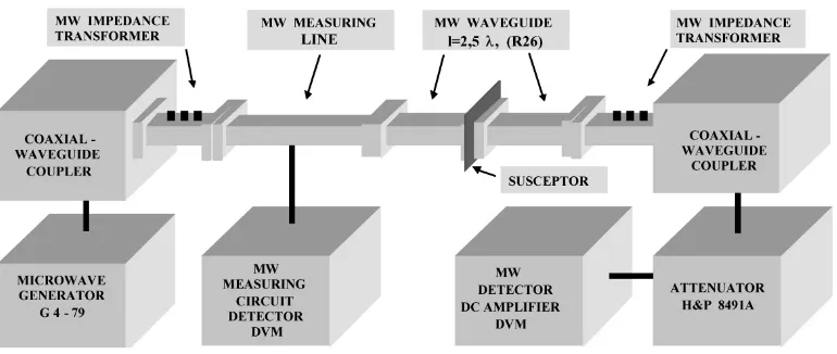
A set of susceptor samples of various optical densities was placed into a microwave measure-ment waveguide which was set up especially for the purpose of this study, and whose arrangement is demonstrated in Figure 3. The measurement was carried out at the frequency of 2.45 GHz and the applied microwave power of 1.8 mW. The values of the reflected, transmitted and absorbed power in the susceptor samples as well as the values of the surface impedance were determined.
All results presented in this work are the mean values of two parallel determinations unless dif-ferent conditions are given.
RESULTS AND CONCLUSIONS Optical and electrical parameters of susceptors
and their relationship
The proper susceptor function in the microwave field is dependent on the thickness of the metal layer. The Al layers suitable for susceptors (up to about 10 nm thick) contain a large number of holes, thickness non-homogeneities, steps and micro-cracks. This makes the direct and exact de-termination of the layer thickness very difficult (S��������� et al. 2001). Therefore, optical density (absorbance) and/or DC square resistance are fre-quently used for the thickness description of thin metallic layers of susceptors. For the preparation
of susceptors the relation between both parameters may be important but little information on that problem has been published.
The relationship between DC square resistance and the mean value of optical density of the suscep-tors tested is presented in Figure 4. As obvious, the square resistance of the samples tested varies from 25 to 500 Ω in the range of the optical density of the samples from 0.15 to 0.6. The relatively higher variance of the results is caused by the uncertainty in the determination of the layer optical density resulting from the non-uniformity of the thick-ness of the laboratory prepared susceptors as well as by the measurements of the square resistance (the layers contain a large number of electrically active defects).
The correlation between DC square resistance (RS) and optical density (O.D.) can be expressed by the following regression equation:
RS = 745.8 e–6.43(O.D.) (6)
the regression quotient r2 = 0.727
It is obvious from the regression curve that DC square resistance in the range from 100 Ω to 230 Ω cor-responds to the range of the optical density of commercially produced susceptors from 0.18 to 0.29 (S���� et al. 1990). This is in a good agreement with the literature data – the value of 188.5 Ω is presented in literature as the square resistance of the susceptors of the most efficient microwave absorption (B������ 1993).
[image:4.595.113.498.83.246.2]the surface of susceptor samples. On this base the theoretical thickness of homogeneous layer of Al can be calculated using specific weight of aluminium ρ = 2.71 g/cm3. The relationship between
the calculated theoretical Al layer thickness (AlT) and the mean value of the optical density (O.D.) of susceptor samples is presented in Figure 5. The correlation can be expressed by the following re-gression equation:
AlT = 15.09 (O.D.) + 2.01 (7)
the regression quotient r2 = 0.9471
The mean value of the optical density of the pre-pared Al susceptors in the range from 0.05 to 0.5 corresponds to the theoretical Al layer thickness from 3 to 10 nm which is in good agreement with the presumption that the thickness of Al layer of suscep-tors is smaller than 10 nm (R�������� 1993).
[image:5.595.66.279.82.246.2] [image:5.595.309.520.98.245.2]For comparison, three samples of laboratory prepared susceptors were analysed in the Depart-ment of Nuclear Physics of the Czech Academy of Sciences by Rutherford Back Scattering Technique and similar results were obtained: the metal deposit thickness on the susceptors of 3.5 nm, 4.8 nm and Figure 5. Thickness vs. optical density of Al layer
Figure 6. Reflected (PR), transmi�ed (PT) and absorbed (PA) microwave power ratio vs. optical density of sus-ceptors
Figure 4. DC square resistance vs. optical density �
�� ��� ��� ��� ��� ���
��� ��� ��� ��� ��� ���
���������������
����
�������
�����������
����
0 4 8 12 16 20
0.0 0.2 0.4 0.6 0.8 1.0 1.2
Optical density
Th
ic
kn
es
s
(n
m
)
UV/VIS Spectrometer Perkin Elmer at 620 nm
��� ��� ��� ��� ��� ���
���� ���� ���� ���� ����
���������������
����������
������
�����
��������������������
������������������
�����������������
[image:5.595.96.489.487.718.2]5.5 nm corresponded to the optical density values of 0.19, 0.21 and 0.28, respectively.
Microwave measurement
As a result of these measurements, the dependen-cies between the reflected, transmitted and, finally, absorbed power in the susceptors and their optical densities were obtained. The maximal value of the absorbed microwave power PA = 48% corresponds to the susceptors having the optical density of about 0.22 (Figure 6). The curves in the graph were constructed using polynomial approxima-tion. Under all conditions, the following equation must be valid
PT + PR + PA = 1 (8)
As mentioned above, the surface impedance Z
most essentially describes the nature of the metal-lized film interaction with the microwave field. The microwave measurements also enabled to estimate the dependence of the susceptor surface impedance on its optical density. This dependence is presented in Figure 7. The correlation can be expressed by the following regression equation:
Zn = 8894.7 (O.D.)4 + 11 394 (O.D.)3 + 5430.5 (O.D.)2 +
+ 1142.9 (O.D.) + 89.9 (9)
the regression quotient r2 = 0.9876
By comparison of the results of DC square resist-ance determination with the data on the microwave square impedance Zsit is obvious that the main part of the total surface impedance is created by its real part, i.e. DC square resistance. The surface impedance (Zs) of the susceptors commonly used in food packaging and having optical density of about 0.18–0.29 (B������ 1993) should range from 70 Ω to 1150 Ω.
References
B������ C.R. (1993): Microwave Cooking and Proces-sing. An Avi Book. Van Norstrand Reinbold Publ., New York.
G�������� V.V. (1998): Microwave Nondestructive Te-sting of Thin Multi-layers of Conductive Structures. In: Proc. 1st Pan Am. Conf. Nondestructive Testing, Toronto.
K����� CH. (1985): Úvod do fyziky pevných látek. Aca-demia, Praha.
P������� B.B., S������ B.S. (1986): Materials for Electronics. Vysšaja škola, Moscow. (in Russian) R�������� G.L. (1993): Food Packaging. Principles
and Practice. M. Dekker, Basel: 409–430.
S������� R. (2001): Měřič optické hustoty. [Diploma thesis.] CTU Prague.
S��������� Y., Y������� N., S��������� L.J. (2001): Ultra-thin Eitaxial Films of Al and Cu Grown on CaF2/Si (111); www.rpi.edu/~schowl/mbe/research.
S���� J.P., R�������� H.S., S������ B.K. (1990): Developments in Food Packaging Technology. Part 1. Trends Food Sci. Technol., Nov.: 107–110.
S��������� E.H. (1952): The mean free path of electrons in metals. Adv. Phys., 1: 1–5.
Z�������� H., M���� J. (1992): Characterization of thin-layer susceptor for the microwave oven. J. Process. Preserv., 16: 193–204.
Z�������� H., M���� J. (1994): Changes in thin-layer susceptors during microwave heating. Packaging Technol. Sci., 7: 21–26.
[image:6.595.306.528.87.239.2]Received for publication October 22, 2002 Accepted a�er corrections February 12, 2003 Figure 7. Normalized surface impedance of susceptor vs. its optical density
Souhrn
Č����� J., D����� J., H������ J., S������� J. (2003): Vlastnosti tenkých kovových vrstev pro mikrovlnné suscep-tory. Czech J. Food Sci., 21: 34–40.
Tenké vrstvy hliníku v tloušťkách od 3 do 30 nm byly naneseny na polyethylentereftalátovou fólii napařováním ve vakuu (3 × 10⁻³ Pa). Povrchový odpor takto připravených fólií byl proměřen čtyřbodovou metodou a byla stanovena
��� ��� ��� ��� ��� ��� ��� ��� ���
���� ��� ���� ���
���������������
���������������������
��
�������������������
jeho závislost na tloušťce hliníkové vrstvy. Přitom byl patrný tzv. „size effect“ v souladu s Fuchs-Sondheimerovou teorií. Schopnost absorbovat mikrovlnnou energii u připravených fólií s rozdílnou úrovní pokovení byla stanovena v mikrovlnném poli při mikrovlnném výkonu 1,8 mW. Bylo zjištěno, že maximální absorpci mikrovlnné energie při frekvenci 2,45 GHz vykazují fólie s optickou hustotou 0,22.
Klíčová slova: mikrovlnný ohřev; susceptory; balení potravin; optická hustota; DC povrchový odpor; absorpce mikrovln
Corresponding author:
Doc. Ing. J������� D�����, CSc., Vysoká škola chemicko-technologická, Ústav konzervace potravin a technologie masa, Technická 5, 166 28 Praha 6, Česká republika