( DOC No. HX8238-A -AN )
HX8238-A
960 x 240 TFT LCD Single Chip
Digital Driver
1. General Description
The HX8238-A application note includes SPI commands, FPC pins, OLB resistance and application circuit. H-Sync (HSYNC), V-Sync (VSYNC), Data enable (DEN), and Clock (DOTCLK) from video decoder or other source.The interface follows digital 8-bit serial/24-bit parallel RGB, CCIR601 and CCIR656 input format.
HX8238-A is a single chip controller and driver LSI that integrated the power circuit. It can drive a maximum 960x240 dot graphics on a-TFT panel displays in 262K colors. HX8238-A has a low-voltage operation, 1.4 min. In addition, HX8238-A is equipped with a DC-DC converter control circuit that generates the supply voltage for source and gate drivers with minimum external components. A common voltage generation circuit is included to drive the TFT-display counter electrode. An integrated gamma control circuit is also included that can be adjusted by software commands to provide maximum flexibility and optimal display quality.
960 x 240 TFT LCD Single Chip Digital
Driver
Preliminary Version 01
2.SPI commands setting
2.1 Serial Interface
The SPI is available through the chip select line (CSB), serial transfer clock line (SCK), serial data input (SDI), and serial data output (SDO).
The Driver IC recognizes the start of data transfer at the falling edge of CSB input to initiate the transfer of start byte. It recognizes the end of data transfer at the rising edge of CSB input. The Driver IC is selected when the 6-bit chip address in the start byte transferred from the transmission device and the 6-bit device identification code assigned to the Driver IC are compared and both 6-bit data correspond. The identification code must be 011100. Two different chip addresses must be assigned to the Driver IC because the seventh bit of the start byte is assigned to a register select bit (RS). When RS = 0, index register write or status read is executed. When the RS = 1, instruction write. The eighth bit of the start byte is to specify read or write (R/W bit). The data are received when the R/W bit is 0, and are transmitted when the R/W bit is 1.
After receiving the start byte, the Driver IC starts to transmit or receive data by byte. The data transmission adopts a format by which the MSB is first transmitted (9th SCK started). All Driver IC instructions consist of 16 bits and they are executed internally after two bytes are transmitted with the MSB first (IB15 to 0---9th ~24th SCK).
1 2 3 4 5 6 7 8 9 10 11 12 13 14 15 16 17 18 19 20 21 22 23 24 0 RS RW CSB SDI 1 1 1 DB 15 DB 14 DB 13 DB 12 DB 11 DB 10 DB 9 DB 8 DB 7 DB 6 DB 5 DB 4 DB 3 DB 2 DB 1 DB 0 0 0 MSB LSB DB 15 DB 14 DB 13 DB 12 DB 11 DB 10 DB 9 DB 8 DB 7 DB 6 DB 5 DB 4 DB 3 DB 2 DB 1 DB 0 Device ID Index register setting/Instruction
Status read
SDO
Transfer starts Transfer ends
SCK
AN Preliminary V01
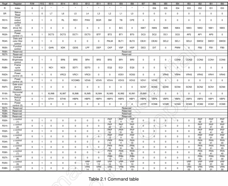
2.2 Command Table
Reg# Register R/W R/S IB15 IB14 IB13 IB12 IB11 IB10 IB9 IB8 IB7 IB6 IB5 IB4 IB3 IB2 IB1 IB0
R Index 0 0 * * * * * * * * * ID6 ID5 ID4 ID3 ID2 ID1 ID0
SR Status Read 1 0 L7 L6 L5 L4 L3 L2 L1 L0 0 0 0 0 0 0 0 0
R01h Driver output control
0 1 0 RL REV PINV BGR SM TB CPE 0 0 0 0 0 0 0 0
R02h LCD driver AC
control
0 1 0 0 0 0 0 0 B/C 0 NW7 NW6 NW5 NW4 NW3 NW2 NW1 NW0
R03h control (1) Power 0 1 DCT3 DCT2 DCT1 DCT0 BTF BT2 BT1 BT0 DC3 DC2 DC1 DC0 AP2 AP1 AP0 0
R04h Data and color filter control
0 1 0 0 0 0 0 PALM BLT1 BLT0 OEA1 OEA0 SEL2 SEL1 SEL0 SWD2 SWD1 SWD0
R05h Function
control 0 1 GHN XDK GDIS LPF DEP CKP VSP HSP DEO DIT 0 PWM 0 FB2 FB1 FB0
R06h Reserved Reserved R07h Reserved Reserved R0Ah Contrast/ Brightness control
0 1 0 BR6 BR5 BR4 BR3 BR2 BR1 BR0 0 0 0 CON4 CON3 CON2 CON1 CON0
R0Bh Frame
cycle control
0 1 NO1 NO0 SDT1 SDT0 0 EQ2 EQ1 EQ0 0 0 0 0 0 0 0 0
R0Dh control (3) Power 0 1 0 VRC2 VRC1 VRC0 0 0 VDS1 VDS0 0 0 VRH5 VRH4 VRH3 VRH2 VRH1 VRH0
R0Eh control (4) Power 0 1 0 0 VCOMG VDV6 VDV5 VDV4 VDV3 VDV2 VDV1 VDV0 0 0 0 0 0 0
R0Fh
Gate scan starting Position
0 1 0 0 0 0 0 0 0 0 SCN7 SCN6 SCN5 SCN4 SCN3 SCN2 SCN1 SCN0
R16h Horizontal Porch 0 1 XLIM8 XLIM7 XLIM6 XLIM5 XLIM4 XLIM3 XLIM2 XLIM1 XLIM0 0 0 0 0 0 0 0
R17h Vertical Porch 0 1 STH1 STH0 HBP6 HBP5 HBP4 HBP3 HBP2 HBP1 HBP0 VBP6 VBP5 VBP4 VBP3 VBP2 VBP1 VBP0
R1Eh control (5) Power 0 1 0 0 0 0 0 0 0 0 nOTP VCM6 VCM5 VCM4 VCM3 VCM2 VCM1 VCM0
R27h Reserved Reserved R28h Reserved Reserved R29h Reserved Reserved R2Bh Reserved Reserved R30h γ control (1) 0 1 0 0 0 0 0 PKP 12 PKP 11 PKP 10 0 0 0 0 0 PKP 02 PKP 01 PKP 00 R31h γ control (2) 0 1 0 0 0 0 0 PKP 32 PKP 31 PKP 30 0 0 0 0 0 PKP 22 PKP 21 PKP 20 R32h γ control (3) 0 1 0 0 0 0 0 PKP 52 PKP 51 PKP 50 0 0 0 0 0 PKP 42 PKP 41 PKP 40 R33h γ control (4) 0 1 0 0 0 0 0 PRP 12 PRP 11 PRP 10 0 0 0 0 0 PRP 02 PRP 01 PRP 00 R34h γ control (5) 0 1 0 0 0 0 0 PKN 12 PKN 11 PKN 10 0 0 0 0 0 PKN 02 PKN 01 PKN 00 R35h γ control (6) 0 1 0 0 0 0 0 PKN 32 PKN 31 PKN 30 0 0 0 0 0 PKN 22 PKN 21 PKN 20 R36h γ control (7) 0 1 0 0 0 0 0 PKN 52 PKN 51 PKN 50 0 0 0 0 0 PKN 42 PKN 41 PKN 40 R37h γ control (8) 0 1 0 0 0 0 0 PRN 12 PRN 11 PRN 10 0 0 0 0 0 PRN 02 PRN 01 PRN 00 R3Ah γ control (9) 0 1 0 0 0 VRP 14 VRP 13 VRP 12 VRP 11 VRP 10 0 0 0 0 VRP 03 VRP 02 VRP 01 VRP 00 R3Bh γ control (10) 0 1 0 0 0 VRN 14 VRN 13 VRN 12 VRN 11 VRN 10 0 0 0 0 VRN 03 VRN 02 VRN 01 VRN 00
2.3 Driver Output Control (R01h)
R/W RS IB15 IB14 IB13 IB12 IB11 IB10 IB9 IB8 IB7 IB6 IB5 IB4 IB3 IB2 IB1 IB0 W 1 0 R L REV PINV BGR S M T B CPE 0 0 1 1 1 1 1 1
Figure 2.2 Driver output control
CPE: When CPE=0, internal charge pump circuit is shut down. When CPE=1, internal charge pump circuit is enabled.
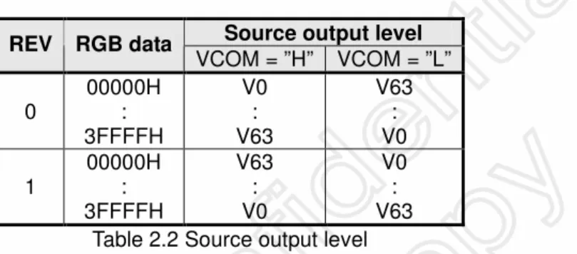
REV: Displays all character and graphics display sections with reversal when REV =
“1”. Since the grayscale level can be reversed, display of the same data is enabled on normally white and normally black panels. Source output level is indicated below.
Source output level REV RGB data VCOM = ”H” VCOM = ”L” 0 00000H : 3FFFFH V0 : V63 V63 : V0 1 00000H : 3FFFFH V63 : V0 V0 : V63 Table 2.2 Source output level
PINV: When PINV=0, POL output is same phase with internal VCOM signal. When
PINV=1, POL output phase is reversed with VCOM signal.
BGR: Selects the <R><G><B> arrangement. When BGR = “0” <R><G><B> color is
assigned from S0.When BGR = “1” <B><G><R> color is assigned from S0.
SM: Change the division of gate driver. When SM = “0”, odd/even division (interlace mode) is selected. When SM = “1”, upper/lower division is selected. Select the division mode according to the mounting method.
TB: Selects the output shift direction of the gate driver. When TB = “1”, G0 shifts to G239. When TB = “0”, G239 shifts to G0.
RL: Selects the output shift direction of the source driver. When RL = “1”, S0 shifts to S959 and <R><G><B> color is assigned from S0. When RL = “0”, S959 shifts to S0 and <R><G><B> color is assigned from S959. Set RL bit and BGR bit when changing the dot order of R, G and B.
Note: The default setting of register bits REV, BGR, TB and RL are defined by the logic stage of corresponding hardware
AN Preliminary V01 SM = 0 SM = 1 TB = 1 RL = 1 G0 S0 S959 G2 G4 G1 G3 G5 G237 G239 G236 G238 G 0 S959 S0 G2 G4 G 1 G 3 G 5 G237 G239 G 236 G 238 TB = 0 RL = 1 236 238 G 0 S959 S0 G2 G4 G 1 G 3 G 5 G237 G239 G G G 0 S959 S0 G2 G4 G 1 G 3 G 5 G 237 G 239 G 236 G 238 TB = 1 RL = 0 G 0 S959 S0 G2 G4 G 1 G 3 G 5 G237 G239 G 236 G 238 G0 S959 S0 G2 G4 G1 G3 G5 G237 G239 G236 G238 TB = 0 RL = 0 G 0 S959 S0 G2 G4 G 1 G 3 G 5 G237 G239 G 236 G 238 G0 S959 S0 G2 G4 G 1 G 3 G 5 G237 G239 G236 G238
2.4 LCD-Driving-Waveform Control (R02h)
R/W RS IB15 IB14 IB13 IB12 IB11 IB10 IB9 IB8 IB7 IB6 IB5 IB4 IB3 IB2 IB1 IB0 W 1 0 0 0 0 0 0 B / C 0 NW7 MW6 NW5 NW4 NW3 NW2 NW1 NW0
Figure 2.3 LCD-driving-waveform control
B/C: When B/C = 0, frame inversion of the LCD driving signal is enabled. When B/C =
1, a N-line inversion waveform is generated and alternates in each N lines specified by bits NW7-0.
NW7-0: Specify the number of lines that will alternate at the N-line inversion setting
(B/C = 1). NW7-0 alternate for every set value + 1 line.
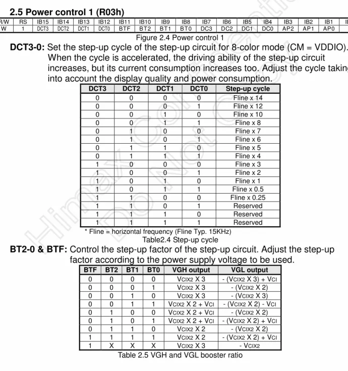
2.5 Power control 1 (R03h)
R/W RS IB15 IB14 IB13 IB12 IB11 IB10 IB9 IB8 IB7 IB6 IB5 IB4 IB3 IB2 IB1 IB0 W 1 DCT3 DCT2 DCT1 DCT0 BTF BT2 BT1 BT0 DC3 DC2 DC1 DC0 AP2 AP1 AP0 0
Figure 2.4 Power control 1
DCT3-0: Set the step-up cycle of the step-up circuit for 8-color mode (CM = VDDIO).
When the cycle is accelerated, the driving ability of the step-up circuit
increases, but its current consumption increases too. Adjust the cycle taking into account the display quality and power consumption.
DCT3 DCT2 DCT1 DCT0 Step-up cycle 0 0 0 0 Fline x 14 0 0 0 1 Fline x 12 0 0 1 0 Fline x 10 0 0 1 1 Fline x 8 0 1 0 0 Fline x 7 0 1 0 1 Fline x 6 0 1 1 0 Fline x 5 0 1 1 1 Fline x 4 1 0 0 0 Fline x 3 1 0 0 1 Fline x 2 1 0 1 0 Fline x 1 1 0 1 1 Fline x 0.5 1 1 0 0 Fline x 0.25 1 1 0 1 Reserved 1 1 1 0 Reserved 1 1 1 1 Reserved
* Fline = horizontal frequency (Fline Typ. 15KHz) Table2.4 Step-up cycle
BT2-0 & BTF: Control the step-up factor of the step-up circuit. Adjust the step-up
factor according to the power supply voltage to be used.
BTF BT2 BT1 BT0 VGH output VGL output 0 0 0 0 VCIX2 X 3 - (VCIX2 X 3) + VCI 0 0 0 1 VCIX2 X 3 - (VCIX2 X 2) 0 0 1 0 VCIX2 X 3 - (VCIX2 X 3) 0 0 1 1 VCIX2 X 2 + VCI - (VCIX2 X 2) - VCI 0 1 0 0 VCIX2 X 2 + VCI - (VCIX2 X 2) 0 1 0 1 VCIX2 X 2 + VCI - (VCIX2 X 2) + VCI 0 1 1 0 VCIX2 X 2 - (VCIX2 X 2) 1 1 1 1 VCIX2 X 2 - (VCIX2 X 2) + VCI 1 X X X VCIX2 X 3 - VCIX2
AN Preliminary V01
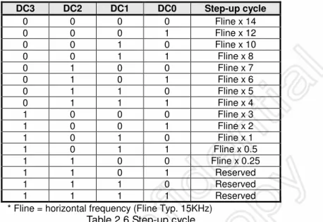
DC3-0: Set the step-up cycle of the step-up circuit for 262k-color mode (CM = VSS).
When the cycle is accelerated, the driving ability of the step-up circuit increases, but its current consumption increases too. Adjust the cycle taking into account the display quality and power consumption.
DC3 DC2 DC1 DC0 Step-up cycle 0 0 0 0 Fline x 14 0 0 0 1 Fline x 12 0 0 1 0 Fline x 10 0 0 1 1 Fline x 8 0 1 0 0 Fline x 7 0 1 0 1 Fline x 6 0 1 1 0 Fline x 5 0 1 1 1 Fline x 4 1 0 0 0 Fline x 3 1 0 0 1 Fline x 2 1 0 1 0 Fline x 1 1 0 1 1 Fline x 0.5 1 1 0 0 Fline x 0.25 1 1 0 1 Reserved 1 1 1 0 Reserved 1 1 1 1 Reserved
* Fline = horizontal frequency (Fline Typ. 15KHz) Table 2.6 Step-up cycle
AP2-0: Adjust the amount of current from the stable-current source in the internal
operational amplifier circuit. When the amount of current becomes large, the driving ability of the operational-amplifier circuits increase. Adjust the current taking into account the power consumption. During times when there is no display, such as when the system is in a sleep mode, set AP2-0 = “000” to halt the operational amplifier circuit and the step-up circuits to reduce current consumption.
AP2 AP1 AP0 Op-amp power
0 0 0 Least 0 0 1 Small 0 1 0 Small to medium 0 1 1 Medium 1 0 0 Medium to large 1 0 1 Large 1 1 0 Large to Maximum 1 1 1 Maximum
2.6 Input Data and Color Filter Control (R04h)
R/W RS IB15 IB14 IB13 IB12 IB11 IB10 IB9 IB8 IB7 IB6 IB5 IB4 IB3 IB2 IB1 IB0 W 1 0 0 0 0 0 PALM BLT1 BLT0 OEA1 OEA0 SEL2 SEL1 SEL0 SWD2 SWD1 SWD0
Figure2.5 Input data and color filter control
SWD2-0: Control and switch the relationship between the R, G, B data and color filter type.
R G B R G B R G B G B R B R G B R G R G B R G B R G B G B R R G B R G B R G B G B R … … SWD[2:0]= 000 SWD [2:0]= 001 R G B G B R SWD [2:0]=01X SWD[2:0]= 100 R G B G B R SWD [2:0]= 101 R G B G B R R G B R G B R G B G B R SWD [2:0]= 110 R G B R G B SWD[ 2:0]= 111 R G B R G B R G B R G B R G B G B R R G B R G B R G B G B R R G B R G B R G B G B R G1 G2 G3 G4 G240 G237 G238 G239 QXH L H L H L H L H R G B G B R R G B G B R … … R G B G B R R G B G B R R G B G B R R G B G B R G1 G2 G3 G4 G240 G237 G238 G239 QXH L H L H L H L H R G B R G B R G B G B R … … R G B R G B R G B G B R R G B R G B R G B G B R G1 G2 G3 G4 G 240 G237 G238 G239 QXH L H L H L H L H R G B R G B R G B G B R … … R G B R G B R G B G B R R G B R G B R G B G B R G1 G2 G3 G4 G240 G237 G238 G239 QXH L H L H L H L H R G B G B R R G B G B R … … R G B G B R R G B G B R R G B G B R R G B G B R G1 G2 G3 G4 G 240 G237 G238 G239 QXH L H L H L H L H R G B R G B R G B G B R … … R G B R G B R G B G B R R G B R G B R G B G B R G1 G2 G3 G4 G240 G 237 G238 G 239 QXH L H L H L H L H R G B R G B R G B R G B … … R G B R G B R G B R G B R G B R G B R G B R G B G1 G2 G3 G4 G240 G237 G238 G239 QXH L L L L L L L L
Note:The QXH is used to control the input data sequence.
2 4 0 L in e s 2 3 4 L in e s 2 4 0 L in e s 2 3 4 L in e s 2 4 0 L in e s 2 3 4 L in e s 2 4 0 L in e s 2 3 4 L in e s 2 4 0 L in e s 2 3 4 L in e s 2 4 0 L in e s 2 3 4 L in e s 2 4 0 L in e s 2 3 4 L in e s
Table 2.8 Color filter type.
SEL2-0: Define the input interface mode.
SEL2 SEL1 SEL0 Format Operating Frequency
0 0 0 Parallel-RGB data format
(only support stripe type color filter) 6.5MHz
0 0 1 Serial-RGB data format 19.5MHz
0 1 0 CCIR 656 data format (640RGB) 24.54MHz
0 1 1 CCIR 656 data format (720RGB) 27MHz
1 0 0 YUV mode A data format (Cr-Y-Cb-Y) 24.54MHz 1 0 1 YUV mode A data format (Cr-Y-Cb-Y) 27MHz 1 1 0 YUV mode B data format (Cb-Y-Cr-Y) 27MHz 1 1 1 YUV mode B data format (Cb-Y-Cr-Y) 24.54MHz
Input format DOTCLK Freq (MHz) Display Data Active Area (DOTCLK)
24.54 640 1280
YUV mode
27 720 1440
AN Preliminary V01
OEA1-0: Odd/Even filed advanced function.
OEA1 OEA0
0 0 Display Start @ VBP delay for Odd field and @ VBP-1 for Even field.
0 1 Display Start @ VBP delay for Odd field and @ VBP for Even field.
1 0 Display Start @ VBP delay for Odd field and @ VBP+1 for Even field.
1 1 No use
Table 2.10 Odd/even filed advanced function.
BLT[1:0]: Set the initial power on black image insertion time. 00: 10 fields
01: 20 fields 10: 40 fields 11: 80 fields
PALM: Set the input data line number in PAL mode 0: 280 lines
1: 288 lines
2.7 Function Control (R05h)
R/W RS IB15 IB14 IB13 IB12 IB11 IB10 IB9 IB8 IB7 IB6 IB5 IB4 IB3 IB2 IB1 IB0 W 1 GHN XDK GDIS LPF DEP CKP VSP HSP DEO D I T 0 PWM 0 FB2 FB1 FB0
Figure 2.6 Function control
FB2-0: Set PWM feedback level adjustment. 000: 0.4V 001: 0.45V 010: 0.5V 011: 0.55V 100: 0.6V 101: 0.65V 110: 0.7V 111: 0.75V
PWM: When PWM=0, PWM function is disabled. When PWM=1, PWM function is enabled.
DIT: When DIT=0, dithering function is turned off. When DIT=1, dithering function is enabled.
DEO: When DEO=0, VSYNC/HSYNC are also needed in DE mode. Under this
condition, vertical back porch is defined by VBP[6:0] and the horizontal first valid data is defined by DE signal. When DEO=1, only DEN signal is needed in DE mode.
HSP: When HSP=0, HSYNC is negative polarity. When HSP=1, HSYNC is positive polarity.
VSP: When VSP=0, VSYNC is negative polarity. When VSP=1, VSYNC is positive polarity.
CKP: When CKP=0, data is latched in CLK falling edge. When CKP=1, data is latched by CLK rising edge.
DEP: When DEP=0, DEN is negative polarity active. When DEP=1, DEN is positive polarity active.
LPF: When LPF=0, the low pass filter function in YUV mode is disabled. When LPF=1, the low pass filter function is YUV mode is enabled.
GDIS: When GDIS=0, VGL has no discharge path to VSS in standby mode. When GDIS=1, VGL will discharge to VSS in standby mode.
XDK: When XDK=0, VCIX2 is 2 stage pumping from VCI. (VCIX2=3 x VCI) When XDK=1, VCIX2 is 2 phase pumping from VCI. (VCIX2=2 x VCI)
GHN: When GHN=0, all gate outputs are forced to VGH. When GHN=1, gate driver is normal operation.
2.8 Contrast/Brightness Control (R0Ah)
R/W RS IB15 IB14 IB13 IB12 IB11 IB10 IB9 IB8 IB7 IB6 IB5 IB4 IB3 IB2 IB1 IB0 W 1 0 BR6 BR5 BR4 BR3 BR2 BR1 BR0 0 0 0 CON4 CON3 CON2 CON1 CON0
Figure 2.7 Contrast/Brightness control
CON4-0: Display Contrast level adjustment. (0.125/step) Adjust range from 00h(level = 0)
to 1Fh(level = 3.875). Default value is 08h(level = 1).
BR6-0: Display Brightness level adjustment. (2/step) Adjust range from 00h(level = -128)
to 7Fh(level = +126). Default value is 40h(level = 0).
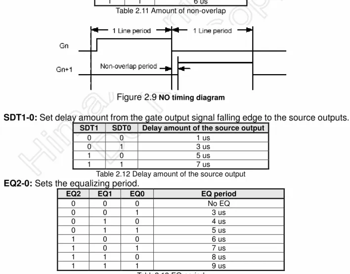
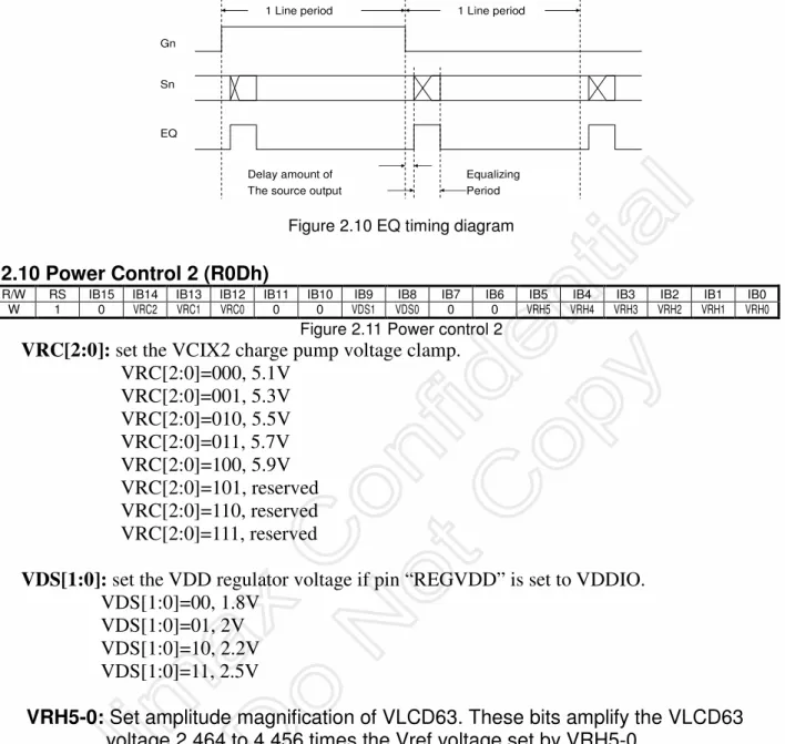
2.9 Frame Cycle Control (R0Bh)
R/W RS IB15 IB14 IB13 IB12 IB11 IB10 IB9 IB8 IB7 IB6 IB5 IB4 IB3 IB2 IB1 IB0 W 1 N O 1 NO0 SDT1 SDT0 0 EQ2 EQ1 EQ0 0 0 0 0 0 0 0 0
Figure2.8 Frame cycle control
NO1-0: Sets amount of non-overlap of the gate output.
NO1 NO0 Amount of non-overlap
0 0 1.5 us
0 1 3 us
1 0 4.5 us
1 1 6 us
Table 2.11 Amount of non-overlap
Figure 2.9 NO timing diagram
SDT1-0: Set delay amount from the gate output signal falling edge to the source outputs.
SDT1 SDT0 Delay amount of the source output
0 0 1 us
0 1 3 us
1 0 5 us
1 1 7 us
Table 2.12 Delay amount of the source output
EQ2-0: Sets the equalizing period.
EQ2 EQ1 EQ0 EQ period
0 0 0 No EQ 0 0 1 3 us 0 1 0 4 us 0 1 1 5 us 1 0 0 6 us 1 0 1 7 us 1 1 0 8 us 1 1 1 9 us Table2.13 EQ period
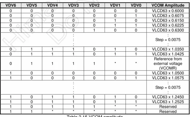
AN Preliminary V01
1 Line period 1 Line period Gn
Sn EQ
Delay amount of The source output
Equalizing Period
Figure 2.10 EQ timing diagram 2.10 Power Control 2 (R0Dh)
R/W RS IB15 IB14 IB13 IB12 IB11 IB10 IB9 IB8 IB7 IB6 IB5 IB4 IB3 IB2 IB1 IB0 W 1 0 VRC2 VRC1 VRC0 0 0 VDS1 VDS0 0 0 VRH5 VRH4 VRH3 VRH2 VRH1 VRH0
Figure 2.11 Power control 2
VRC[2:0]: set the VCIX2 charge pump voltage clamp. VRC[2:0]=000, 5.1V VRC[2:0]=001, 5.3V VRC[2:0]=010, 5.5V VRC[2:0]=011, 5.7V VRC[2:0]=100, 5.9V VRC[2:0]=101, reserved VRC[2:0]=110, reserved VRC[2:0]=111, reserved
VDS[1:0]: set the VDD regulator voltage if pin “REGVDD” is set to VDDIO. VDS[1:0]=00, 1.8V
VDS[1:0]=01, 2V VDS[1:0]=10, 2.2V
VDS[1:0]=11, 2.5V
VRH5-0: Set amplitude magnification of VLCD63. These bits amplify the VLCD63
voltage 2.464 to 4.456 times the Vref voltage set by VRH5-0.
VRH5 VRH4 VRH3 VRH2 VRH1 VRH0 VLCD63Voltage VRH5 VRH4 VRH3 VRH2 VRH1 VRH0 VLCD63Voltage 0 0 0 0 0 0 Vref x 2.464 1 0 0 0 0 0 Vref x 3.464 0 0 0 0 0 1 Vref x 2.496 1 0 0 0 0 1 Vref x 3.496 0 0 0 0 1 0 Vref x 2.528 1 0 0 0 1 0 Vref x 3.528 0 0 0 0 1 1 Vref x 2.560 1 0 0 0 1 1 Vref x 3.560 0 0 0 1 0 0 Vref x 2.592 1 0 0 1 0 0 Vref x 3.592 0 0 0 1 0 1 Vref x 2.624 1 0 0 1 0 1 Vref x 3.629 0 0 0 1 1 0 Vref x 2.656 1 0 0 1 1 0 Vref x 3.664 0 0 0 1 1 1 Vref x 2.688 1 0 0 1 1 1 Vref x 3.701 0 0 1 0 0 0 Vref x 2.720 1 0 1 0 0 0 Vref x 3.736 0 0 1 0 0 1 Vref x 2.752 1 0 1 0 0 1 Vref x 3.762 0 0 1 0 1 0 Vref x 2.784 1 0 1 0 1 0 Vref x 3.787 0 0 1 0 1 1 Vref x 2.816 1 0 1 0 1 1 Vref x 3.813 0 0 1 1 0 0 Vref x 2.848 1 0 1 1 0 0 Vref x 3.840 0 0 1 1 0 1 Vref x 2.875 1 0 1 1 0 1 Vref x 3.880 0 0 1 1 1 0 Vref x 2.904 1 0 1 1 1 0 Vref x 3.920 0 0 1 1 1 1 Vref x 2.931 1 0 1 1 1 1 Vref x 3.960 0 1 0 0 0 0 Vref x 2.960 1 1 0 0 0 0 Vref x 4.000 0 1 0 0 0 1 Vref x 2.992 1 1 0 0 0 1 Vref x 4.027
0 1 0 0 1 0 Vref x 3.024 1 1 0 0 1 0 Vref x 4.056 0 1 0 0 1 1 Vref x 3.056 1 1 0 0 1 1 Vref x 4.083 0 1 0 1 0 0 Vref x 3.088 1 1 0 1 0 0 Vref x 4.112 0 1 0 1 0 1 Vref x 3.123 1 1 0 1 0 1 Vref x 4.142 0 1 0 1 1 0 Vref x 3.160 1 1 0 1 1 0 Vref x 4.171 0 1 0 1 1 1 Vref x 3.195 1 1 0 1 1 1 Vref x 4.202 0 1 1 0 0 0 Vref x 3.232 1 1 1 0 0 0 Vref x 4.232 0 1 1 0 0 1 Vref x 3.259 1 1 1 0 0 1 Vref x 4.264 0 1 1 0 1 0 Vref x 3.288 1 1 1 0 1 0 Vref x 4.296 0 1 1 0 1 1 Vref x 3.315 1 1 1 0 1 1 Vref x 4.328 0 1 1 1 0 0 Vref x 3.344 1 1 1 1 0 0 Vref x 4.360 0 1 1 1 0 1 Vref x 3.374 1 1 1 1 0 1 Vref x 4.392 0 1 1 1 1 0 Vref x 3.403 1 1 1 1 1 0 Vref x 4.424 0 1 1 1 1 1 Vref x 3.434 1 1 1 1 1 1 Vref x 4.456
*Vref is the internal reference voltage equals to 1.25V.
Table 2.14 VLCD63 voltage 2.11 Power Control 3 (R0Eh)
R/W RS IB15 IB14 IB13 IB12 IB11 IB10 IB9 IB8 IB7 IB6 IB5 IB4 IB3 IB2 IB1 IB0 W 1 0 0 VCOMG VDV6 VDV5 VDV4 VDV3 VDV2 VDV1 VDV0 0 0 0 0 0 0
Figure 2.12 Power control 3
VCOMG: When VCOMG = “1”, it is possible to set output voltage of VCOML to any level,
and the instruction (VDV6-0) becomes available. When VCOMG = “0”, VCOML output is fixed to VSS level, VCIM output for VCOML power supply stops, and the instruction (VDV6-0) becomes unavailable. Set VCOMG according to the sequence of power supply setting flow as it relates with power supply operating sequence.
VDV6-0: Set the alternating amplitudes of VCOM at the VCOM alternating drive. These
bits amplify VCOM amplitude 0.6 to 1.2525 times the VLCD63 voltage. When VCOMG = “0”, the settings become invalid. External voltage at VCOMR is referenced when VDV = “01111xx”. VDV6 VDV5 VDV4 VDV3 VDV2 VDV1 VDV0 VCOM Amplitude 0 0 0 0 0 0 0 VLCD63 x 0.6000 0 0 0 0 0 0 1 VLCD63 x 0.6075 0 0 0 0 0 1 0 VLCD63 x 0.6150 0 0 0 0 0 1 1 VLCD63 x 0.6225 0 0 0 0 1 0 0 VLCD63 x 0.6300 : : : : Step = 0.0075 : 0 1 1 1 0 1 0 VLCD63 x 1.0350 0 1 1 1 0 1 1 VLCD63 x 1.0425 0 1 1 1 1 * * Reference from external voltage (VCOMR) 1 0 0 0 0 0 0 VLCD63 x 1.0500 1 0 0 0 0 0 1 VLCD63 x 1.0575 : : : : Step = 0.0075 : 1 0 1 1 0 1 0 VLCD63 x 1.2450 1 0 1 1 0 1 1 VLCD63 x 1.2525 1 0 1 1 1 * * Reserved 1 1 * * * * * Reserved
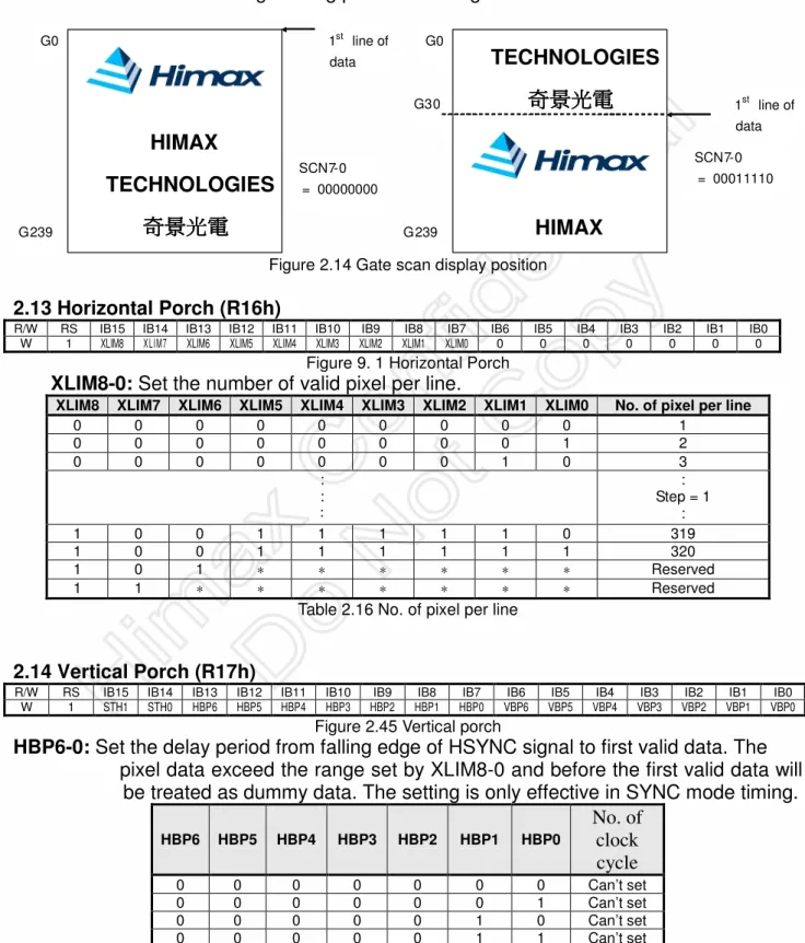
AN Preliminary V01 2.12 Gate Scan Position (R0Fh)
R/W RS IB15 IB14 IB13 IB12 IB11 IB10 IB9 IB8 IB7 IB6 IB5 IB4 IB3 IB2 IB1 IB0 W 1 0 0 0 0 0 0 0 0 SCN7 SCN6 SCN5 SCN4 SCN3 SCN2 SCN1 SCN0
Figure2.13 Gate scan position
SCN8-0: Set the scanning starting position of the gate driver.
HIMAX
TECHNOLOGIES
奇景光電
奇景光電
奇景光電
奇景光電
TECHNOLOGIES
奇景光電
奇景光電
奇景光電
奇景光電
HIMAX
G0 G239 1st line of data SCN7-0 = 00000000 G0 G239 G30 1st line of data SCN7-0 = 00011110Figure 2.14 Gate scan display position 2.13 Horizontal Porch (R16h)
R/W RS IB15 IB14 IB13 IB12 IB11 IB10 IB9 IB8 IB7 IB6 IB5 IB4 IB3 IB2 IB1 IB0 W 1 XLIM8 XLIM7 XLIM6 XLIM5 XLIM4 XLIM3 XLIM2 XLIM1 XLIM0 0 0 0 0 0 0 0
Figure 9. 1 Horizontal Porch
XLIM8-0: Set the number of valid pixel per line.
XLIM8 XLIM7 XLIM6 XLIM5 XLIM4 XLIM3 XLIM2 XLIM1 XLIM0 No. of pixel per line
0 0 0 0 0 0 0 0 0 1 0 0 0 0 0 0 0 0 1 2 0 0 0 0 0 0 0 1 0 3 : : : : Step = 1 : 1 0 0 1 1 1 1 1 0 319 1 0 0 1 1 1 1 1 1 320 1 0 1 ∗ ∗ ∗ ∗ ∗ ∗ Reserved 1 1 ∗ ∗ ∗ ∗ ∗ ∗ ∗ Reserved
Table 2.16 No. of pixel per line
2.14 Vertical Porch (R17h)
R/W RS IB15 IB14 IB13 IB12 IB11 IB10 IB9 IB8 IB7 IB6 IB5 IB4 IB3 IB2 IB1 IB0 W 1 STH1 STH0 HBP6 HBP5 HBP4 HBP3 HBP2 HBP1 HBP0 VBP6 VBP5 VBP4 VBP3 VBP2 VBP1 VBP0
Figure 2.45 Vertical porch
HBP6-0: Set the delay period from falling edge of HSYNC signal to first valid data. The
pixel data exceed the range set by XLIM8-0 and before the first valid data will be treated as dummy data. The setting is only effective in SYNC mode timing.
HBP6 HBP5 HBP4 HBP3 HBP2 HBP1 HBP0 No. of clock cycle 0 0 0 0 0 0 0 Can’t set 0 0 0 0 0 0 1 Can’t set 0 0 0 0 0 1 0 Can’t set 0 0 0 0 0 1 1 Can’t set 0 0 0 0 1 0 0 Can’t set 0 0 0 0 1 0 1 Can’t set 0 0 0 0 1 1 0 Can’t set 0 0 0 0 1 1 1 Can’t set 0 0 0 1 0 0 0 Can’t set 0 0 0 1 0 0 1 9
: Step = 1
:
1 1 1 1 1 1 0 126
1 1 1 1 1 1 1 127
Table 2.17 No. of clock cycle of clock Cycle time of HSYNC
Set by HBP6-0 Set by XLIM8-0
HSYNC
Pixel Data
DOTCLK
Default 320 pixels per line
10 clock cycles of DOTCLK HBP6-0 = 00001000
D0 D1 D2 D317 D318 D319
Dummy Dummy
Figure 2.16No. of clock cycle of clock
STH1-0: Adjust the first valid data by dot clock. This setting is not valid in parallel RGB
input interface.
STH = 00: +0 dot clock
STH = 01: +1 dot clock STH = 10: +2 dot clock STH = 11: +3 dot clock
VBP6-0: Set the delay period from falling edge of VSYNC to first valid line. The line data
within this delay period will be treated as dummy line. The setting is only effective in SYNC mode timing.
VBP6 VBP5 VBP4 VBP3 VBP2 VBP1 VBP0 No. of clock cycle of
HSYNC 0 0 0 0 0 0 0 Can’t set 0 0 0 0 0 0 1 Can’t set 0 0 0 0 0 1 0 2 0 0 0 0 0 1 1 3 0 0 0 0 1 0 0 4 : Step = 1 : 1 1 1 1 1 0 0 124 1 1 1 1 1 0 1 125 1 1 1 1 1 1 0 126 1 1 1 1 1 1 1 127
AN Preliminary V01
Cycle time of VSYNC Set by VBP6-0
VSYNC
HSYNC
Dummy Lines 1st Line Last Line Dummy Lines
Figure 2.17 No. of clock cycle of HSYNC 2.15 Power Control 4 (R1Eh)
R/W RS IB15 IB14 IB13 IB12 IB11 IB10 IB9 IB8 IB7 IB6 IB5 IB4 IB3 IB2 IB1 IB0 W 1 0 0 0 0 0 0 0 0 nOTP VCM6 VCM5 VCM4 VCM3 VCM2 VCM1 VCM0
Figure2.18 Power control 4
nOTP: nOTP equals to “0” after power on reset and VCOMH voltage equals to
programmed OTP value. When nOTP set to “1”, setting of VCM6-0 becomes valid and voltage of VCOMH can be adjusted.
VCM6-0: Set the VCOMH voltage if nOTP = “1”. These bits amplify the VCOMH voltage
0.36 to 0.995 times the VLCD63 voltage.
VCM6 VCM5 VCM4 VCM3 VCM2 VCM1 VCM0 VCOMH 0 0 0 0 0 0 0 VLCD63 x 0.360 0 0 0 0 0 0 1 VLCD63 x 0.365 0 0 0 0 0 1 0 VLCD63 x 0.370 0 0 0 0 0 1 1 VLCD63 x 0.375 0 0 0 0 1 0 0 VLCD63 x 0.380 : : : : : : Step = 0.005 : 1 1 1 1 1 0 0 VLCD63 x 0.980 1 1 1 1 1 0 1 VLCD63 x 0.985 1 1 1 1 1 1 0 VLCD63 x 0.990 1 1 1 1 1 1 1 VLCD63 x 0.995 Note: 2V < VCOMH < VLCD63 Table 2.19 VCOMH
2.16 Gamma Control 1 (R30h to R37h)
R/W RS IB15 IB14 IB13 IB12 IB11 IB10 IB9 IB8 IB7 IB6 IB5 IB4 IB3 IB2 IB1 IB0 W 1 0 0 0 0 0 PKP1 PKP1 PKP1 0 0 0 0 0 PKP0 PKP0 PKP0 W 1 0 0 0 0 0 PKP3 PKP3 PKP3 0 0 0 0 0 PKP2 PKP2 PKP2 W 1 0 0 0 0 0 PKP5 PKP5 PKP5 0 0 0 0 0 PKP4 PKP4 PKP4 W 1 0 0 0 0 0 PRP1 PRP1 PRP1 0 0 0 0 0 PRP0 PRP0 PRP0 W 1 0 0 0 0 0 PKN1 PKN1 PKN1 0 0 0 0 0 PKN0 PKN0 PKN0 W 1 0 0 0 0 0 PKN3 PKN3 PKN3 0 0 0 0 0 PKN2 PKN2 PKN2 W 1 0 0 0 0 0 PKN5 PKN5 PKN5 0 0 0 0 0 PKN4 PKN4 PKN4 W 1 0 0 0 0 0 PRN1 PRN1 PRN1 0 0 0 0 0 PRN0 PRN0 PRN0
Figure 2.19 Gamma control 1
PKP52–00: Gamma micro adjustment register for the positive polarity output.
PRP12-00: Gradient adjustment register for the positive polarity output.
PKN52-00: Gamma micro adjustment register for the negative polarity output.
PRN12-00: Gradient adjustment register for the negative polarity output.
2.17 Gamma Control 2 (R3Ah to R3Bh)
R/W RS IB15 IB14 IB13 IB12 IB11 IB10 IB9 IB8 IB7 IB6 IB5 IB4 IB3 IB2 IB1 IB0 W 1 0 0 0 VRP14 VRP13 VRP12 VRP11 VRP10 0 0 0 0 VRP03 VRP02 VRP01 VRP00 W 1 0 0 0 VRN14 VRN13 VRN12 VRN11 VRN10 0 0 0 0 VRN03 VRN02 VRN01 VRN00
Figure 2.20 Gamma control 2
VRP14-00: Adjustment register for amplification adjustment of the positive polarity
output.
VRN14-00: Adjustment register for the amplification adjustment of the negative polarity
output.
AN Preliminary V01
3.Application Circuit
3.1 PWM Boost Converter C5 47uF/16V Q1 MOSFET N 3400 C7 0.1u L1 22uH TAY IO LB2012T220 C1 47uF R4 27 R1 0 R2 1K C6 2.2uF D2 BZX84C15/SOT R3 1K C4 10uF/16V D1 RB520S-30 VLED-VLED+ VFB C3 1uF/16V C2 0.1uF/16V DRV +3.3VFigure 3.1 PWM Boost Converter
3.2 Booster capacitors CXP CXN CYP CYN C1P C1N C2P C2N C3P C3N CP CN 6.3V 6.3V 6.3V 16V All capacitors are ceramic 0.1~0.33uF 16V 16V
3.3 Power supply pins connections REGVDD = VDDIO 1.8V > System Vdd REGVDD = VSS Regulator VDD VDDIO VCI REGVDD VSS System Vdd Analog power 2.5~3.6V Regulator VDD VDDIO VCI REGVDD VSS System Vdd Analog power 2.5~3.6V System Vdd > 2.5V or 2.5V ≧ System Vdd ≧ 1.8V
AN Preliminary V01 3.4 Filtering and charge sharing capacitors
* VCI * VCIP * VCIM *VCIX2 VLCD63 VGH VGL VCOMH VCOML 6.3V 6.3V 6.3V 6.3V 6.3V 16V 16V 6.3V 6.3V * VSS
Polarity depends on VCOML setting All capacitors are ceramic 1uF 3 schottky barrier diode VF=0.4V/20mA VR=30V
Figure 3.4Filtering and charge sharing capacitors
1.Capacitors on VCI should be 4.7uF. 2.Capactiors on VCIP should be 1uF 3.Capacitor on VCIX2 should be 3.3uF
4.Capacitors on VGH, VGL, VCIM should be 2.2uF 5.Other capacitors should be 1uF
* VCIX2 should be separate with VCIX2J at ITO layout to provide noise free path * VCI should be separate with VCIP at ITO layout to provide noise free path
* VSS should be separate with VCHS, AVSS and VSSRC at ITO layout to provide noise free path
3.5 Panel connection example V C I/ V C IP /V C IX 2 J V S S /A V S S V S S R C /V C H S V D D /V D D IO E x te rn al C o m p o n en t p in s R E S B C S B S C K S D I S D O S H U T C M B G R R E V S W D S E L C P E T B R L
960 X 240
TFT Panel
Cs on Common
G0-G239 S0-S959 VCOM R R [7 :0 ] G G [7 :0 ] B B [7 :0 ] H S Y N C V S Y N C D O T C L K D E N P o w er /G ro u n d R ef er t o f ig u re 3 .1 ~ 3 .4 Q X H P O L M C U s er ia l in te rf ac e an d c o n tr o l H ar d w ar e S et ti n g P in s D u m p d ri v er O u tp u t to c o n tr o l 960 240-P .2 1 - C o n fid e n tia l D e c , 2 0 0 6 rm a tio n c o n ta in e d h e re in is th e e xc lu s iv e p ro p e rty o f H im a x a n d s h a ll n o t b e d is tri b u te d , r e p ro d u c e d , o r d is c lo s e d o r i n p a rt w ith o u t p rio r w rit te n p e rm is s io n o f H im a x. S u b je c t t o c h a n g e w ith o u t n o tic e .
X
8
2
3
8
-A
0 x 2 4 0 T F T L C D S in g le C h ip D ig ita l D riv e r A N P re lim in a ry V 0 1 C a n d G la s s la y o u t w ith in te rn a l c h a rg e p u m b EXVR AVSS VSS EXVR DRV AVSS VSS VCOML VCOMH VCOM VSSRC VCHS VFB C2P C3N C3P VGH VCOMR VDD CN CP VGL C2N CYP CXN CXP VDDIO VCIP VCI C1N VLCD63 VCIX2J VCIX2 CYN SWD2 PINV CPE VCIM C1P BGR SEL0 SEL1 SEL2 SWD0 SWD1 TB REV REGVDD RL CM DEN HSYNC VSYNC SHUT DOTCLK RR2 RR3 RR4 RR5 RR6 RR7 GG5 GG6 GG7 RR0 RR1 GG0 GG1 GG2 GG3 GG4 BB2 BB3 BB4 BB5 BB6 BB7 CSB SCK SDI BB0 BB1 QXH POL SDO RESB U 6 DRV 1 VFB 2 VCHS 3 VSSRC 4 VCOM 5 VCOMH 6 VCOML 7 VCOMR 8 VGH 9 C3P 10 C3N 11 C2P 12 C2N 13 VGL 14 CP 15 CN 16 VDD 17 VCI 18 VCIP 19 VDDIO 20 CXP 21 CXN 22 CYP 23 CYN 24 VCIX2 25 VCIX2J 26 VLCD63 27 C1N 28 C1P 29 VCIM 30 PINV 31 CPE 32 SWD2 33 SWD1 34 SWD0 35 SEL2 36 SEL1 37 SEL0 38 BGR 39 CM 40 RL 41 REGVDD 42 REV 43 TB 44 SHUT 45 DOTCLK 46 VSYNC 47 HSYNC 48 DEN 49 RR7 50 RR6 51 RR5 52 RR4 53 RR3 54 RR2 55 RR1 56 RR0 57 GG7 58 GG6 59 GG5 60 GG4 61 GG3 62 GG2 63 GG1 64 GG0 65 BB7 66 BB6 67 BB5 68 BB4 69 BB3 70 BB2 71 BB1 72 BB0 73 SDI 74 SCK 75 CSB 76 RESB 77 SDO 78 POL 79 QXH 80 VSS 81 EXVR 82 AVSS 83 DRV1 VFB2 VCHS3 VSSRC4 VCOM 5 VCOMH 6 VCOML 7 VCOMR 8 VGH 9 C3P10 C3N 11 C2P12 C2N 13 VGL 14 CP 15 CN 16 VDD 17 VCI 18 VCIP19 VDDIO20 CXP 21 CXN 22 CYP 23 CYN 24 VCIX2 25 VCIX2J 26 VLCD63 27 C1N 28 C1P29 VCIM 30 PINV31 CPE 32 SWD2 33 SWD1 34 SWD0 35 SEL236 SEL137 SEL038 BGR 39 CM 40 RL 41 REGVDD 42 REV 43 TB44 SHUT 45 DOTCLK46 VSYNC47 HSYNC 48 DEN 49 RR7 50 RR6 51 RR5 52 RR4 53 RR3 54 RR2 55 RR1 56 RR0 57 GG7 58 GG6 59 GG5 60 GG4 61 GG3 62 GG2 63 GG1 64 GG0 65 BB7 66 BB6 67 BB5 68 BB4 69 BB3 70 BB2 71 BB1 72 BB0 73 SDI 74 SCK 75 CSB 76 RESB 77 SDO78 POL 79 QXH 80 VSS81 EXVR 82 AVSS83 DRV VFB EXVR VSS VSSRC VCHS VFB DRV AVSS C3P VGH VCOMR VCOML VCOMH VCOM CP VGL C2N C2P C3N VDDIO VCIP VCI VDD CN VCIX2J VCIX2 CYN CYP CXN CXP CPE VCIM C1P C1N VLCD63 SEL2 SWD0 SWD1 SWD2 PINV REGVDD RL CM BGR SEL0 SEL1 VSYNC SHUT DOTCLK TB REV RR5 RR6 RR7 DEN HSYNC GG7 RR0 RR1 RR2 RR3 RR4 VCHS GG2 GG3 GG4 GG5 GG6 BB5 BB6 BB7 GG0 GG1 SDI BB0 BB1 BB2 BB3 BB4 POL SDO RESB CSB SCK QXH VSSRC G la s s 9 6 0 *2 4 0 G 0 0 G 0 2 G 0 3 G 0 1 G 2 3 6 G 2 3 7 G 2 3 8 G 2 3 9 S0 S1 S2 S958 S959 G 0 0 G 0 1 G 0 2 G 0 3 G 2 3 6 G 2 3 7 G 2 3 8 G 2 3 9 S479 S480 S481 S957 VCOM VLED+ VLED-VCOMH VCOML VGH U 7 CO N 8 5 DRV1 VFB2 VCHS3 VSSRC4 VCOM 5 VCOMH6 VCOML7 VCOMR8 VGH 9 C3P10 C3N11 C2P12 C2N13 VGL14 CP15 CN 16 VDD 17 VCI 18 VCIP19 VDDIO20 CXP21 CXN 22 CYP23 CYN 24 VCIX225 VCIX2J 26 VLCD6327 C1N28 C1P29 VCIM 30 PINV31 CPE32 SWD233 SWD134 SWD035 SEL236 SEL137 SEL038 BGR 39 CM40 RL 41 REGVDD 42 REV43 TB44 SHUT 45 DOTCLK46 VSYNC47 HSYNC48 DEN 49 RR750 RR651 RR552 RR453 RR354 RR255 RR156 RR057 GG758 GG659 GG560 GG461 GG362 GG263 GG164 GG065 BB766 BB667 BB568 BB469 BB370 BB271 BB172 BB073 SDI 74 SCK75 CSB76 RESB77 SDO78 POL79 QXH 80 VSS81 EXVR82 AVSS83 VLED+84 VLED-85 VCOMR P A N E L U 5 H X 8 2 3 8 A THROUGH1(1) THROUGH2(1) DUMMY(1) DRV(2) VFB(2) DUMMY(1) VCHS(10) VSSRC(8) VCOM(4) VCOMH(4) VCOML(4) VCOMR(2) TEST16(1) TEST17(1) VGH(5) C3P(3) C3N(3) C2P(3) C2N(3) VGL(5) CP(3) CN(3) DUMMY(1) VDD(6) VCI(6) VCIP(6) VDDIO(6) CXP(6) CXN(6) CYP(6) CYN(6) VCIX2(6) VCIX2J(6) VLCD63(6) C1N(5) C1P(5) VCIM(5) DUMMY(1) PINV(1) CPE(1) VSS(1) SWD2(1) VDDIO(1) SWD1(1) VSS(1) SWD0(1) VDDIO(1) SEL2(1) SEL1(1) SEL0(1) VSS(1) BGR(1) VDDIO(1) CM(1) VSS(1) RL(1) VDDIO(1) REGVDD(1) VSS(1) REV(1) VDDIO(1) TB(1) VSS(1) SHUT(2) DOTCLK(2) VSYNC(2) HSYNC(2) DEN(2) RR7(2) RR6(2) RR5(2) RR4(2) RR3(2) RR2(2) RR1(2) RR0(2) GG7(2) GG6(2) GG5(2) GG4(2) GG3(2) GG2(2) GG1(2) GG0(2) BB7(2) BB6(2) BB5(2) BB4(2) BB3(2) BB2(2) BB1(2) BB0(2) SDI(2) SCK(2) CSB(2) RESB(2) SDO(2) POL(1) QXH(1) DUMMY(1) TEST4(1) TEST5(1) TEST6(1) TEST7(1) TEST8(1) TEST9(1) TEST10(1) TEST11(1) TEST12(1) TEST13(1) TEST14(1) TEST15(1) DUMMY(1) VSS(8) EXVR(4) AVSS(10) DUMMY(1) VCOM(4) DUMMY(1) THROUGH3(1) THROUGH4(1) DUMMY(1) THROUGH5(1) THROUGH6(1) DUMMY(2) G1 G3 G5 G7 G235 G237 G239 DUMMY(6) S0 S1 S2 S3 S955 S957 S958 S959 DUMMY(9) G238 G236 G234 G232 G6 G4 G2 G0 DUMMY(2) THROUGH7(1) THROUGH8(1) DUMMY(1) N o t e : V C O M f o r t e s t C3P C2N C2P C3N CP VGL CN VDD VDDIO VCIP VCI CXP CXN VCIX2 CYN CYP VLCD63 VCIX2J VCIM C1P C1N CPE PINV SWD2 SWD1 SEL2 SWD0 SEL0 SEL1 BGR CM RL REV REGVDD TB DOTCLK SHUT VSYNC HSYNC DEN RR6 RR7 RR3 RR4 RR5 RR0 RR1 RR2 GG6 GG7 GG5 GG4 GG2 GG3 GG0 GG1 BB5 BB6 BB7 BB2 BB3 BB4 BB0 BB1 SDI SCK SDO RESB CSB QXH POL DRV VFB VCHS VSSRC VCOMR VCOML VCOMH VCOM VGH C3N C3P CN CP VGL C2N C2P EXVR VSS VCOM AVSS VDD CXN CXP VDDIO VCIP VCI VLCD63 VCIX2J VCIX2 CYN CYP VCIM C1P C1N CPE PINV SWD2 SWD1 SWD0 SEL2 SEL0 SEL1 BGR CM RL REGVDD REV TB DOTCLK RR7 DEN HSYNC VSYNC SHUT RR2 RR3 RR4 RR5 RR6 GG5 GG6 GG7 RR0 RR1 BB7 GG0 GG1 GG2 GG3 GG4 BB2 BB3 BB4 BB5 BB6 CSB SCK SDI BB0 BB1 QXH POL SDO RESB F ig u re 3 .7 F P C a n d G la s s la y o u t w ith in te rn a l c h a rg e p u m b3.7 FPC, Power connection and LED Backlight Driving Circuit with internal charge pumb CP AVSS CN CP CN EXVR1 CXP CXN CY N CY P CXP CXN VCOML VCOMH VCOM VGL VGH VCOMR DOTCLK VLCD63 VSY NC SDI DEN HSY NC CY P CY N CSB SCK SDO VLED-VLED+ VDDA C1N C1P V D D IO REGVDD RL C1N CM BGR C1P SHUT TB REV VCIX2 VCIX2J VFB DRV VCOM near connector near connector near connector V D D IO SWD1 SWD2 PINV CPE
for VCIX2J from external voltage
for VCOMR from external voltage
Note: The crcuit is on the condition what follows 1.SYSTEM VDD=2.5V~3.6V,REGVDD="H"
2.Strip panel,SWD[2:0]=111
3.Parallel RGB input mode,SEL[2:0]=000 4.from left to right,RL="H"
5.from up to down,TB="H" 6.Normally white,REV="H" 7.Use internal voltage
DRV RESB V D D IO VCIX2J VCIX2 R3 0 C27 0.1u/16V C32 0.1u/16V R19 0 R37 NC C6 10uF R14 0 C33 0.1uF/16V R29 0 T3 JP 1 C31 2.2uF/16V C38 0.1uF/6.3V C23 10uF R26 NC R5 NC L6 BEAD R17 0 R38 NC C26 47uF C30 47uF/16V C8 1uF D2 RB520S-30 C13 10uF VCI R41 0 R24 NC D3 BZX84C15/SOT C17 3.3uF/6.3V R39 NC R7 2K C9 10uF C12 10uF C18 2.2uF/6.3V C21 0.1u C2 2.2uF/16V C5 10uF VCIP R13 NC R1 0 R12 NC R20 0 C29 10uF/16V T2 JP 1 C28 1uF/16V C1 4.7uF/6.3V R25 NC L7 BEAD R8 0 C36 0.1uF/6.3V R40 NC RET1 Q1 MOSFET N 3400 C20 10uF R18 NC VR1 20K 1 3 2 C15 1uF T9 JP 1 C10 2.2uF/16V L5 BEAD T1 JP 1 VCI R30 0 C4 1uF/6.3V R43 0 T4 JP 1 R21 0 R36 NC R35 0 T7 JP 1 D1 RB520-30 R28 0 R16 0 T13JP 1 C39 0.1uF/6.3V T8 JP 1 C35 0.1uF/16V C16 10uF R15 0 R23 0 R11 27 T17JP 1 C22 1uF T14JP 1 R32 NC U1 CON85 DRV 1 VFB 2 VCHS 3 VSSRC 4 VCOM 5 VCOMH 6 VCOML 7 VCOMR 8 VGH 9 C3P 10 C3N 11 C2P 12 C2N 13 VGL 14 CP 15 CN 16 VDD 17 VCI 18 VCIP 19 VDDIO 20 CXP 21 CXN 22 CY P 23 CY N 24 VCIX2 25 VCIX2J 26 VLCD63 27 C1N 28 C1P 29 VCIM 30 PINV 31 CPE 32 SWD2 33 SWD1 34 SWD0 35 SEL2 36 SEL1 37 SEL0 38 BGR 39 CM 40 RL 41 REGVDD 42 REV 43 TB 44 SHUT 45 DOTCLK 46 VSY NC 47 HSY NC 48 DEN 49 RR7 50 RR6 51 RR5 52 RR4 53 RR3 54 RR2 55 RR1 56 RR0 57 GG7 58 GG6 59 GG5 60 GG4 61 GG3 62 GG2 63 GG1 64 GG0 65 BB7 66 BB6 67 BB5 68 BB4 69 BB3 70 BB2 71 BB1 72 BB0 73 SDI 74 SCK 75 CSB 76 RESB 77 SDO 78 POL 79 QXH 80 VSS 81 EXVR 82 AVSS 83 VLED+ 84 VLED-85 C14 0.1u C37 1uF L4 22uH TAY IO LB2012T220 R27 1K T6 JP 1 T15JP 1 T18 JP 1 C3 1uF/6.3V R4 0 VLED+ T10JP 1 R6 5.1K C11 1uF/6.3V C7 0.1u R22 0 R33 NC R2 NC T5 JP 1 R9 1K R34 NC T12JP 1 R31 NC C24 1uF/6.3V C25 2.2uF/6.3V L1 BEAD VLED-L3 BEAD C19 10uF L2 BEAD R42 0 R10 1K T11JP 1 T16JP 1 C34 0.1uF/16V SY STEM VDD 2.5V~3.6V +3.3V 9V 5.0V~6.0V VCIP POL QXH RESB SDO SCK SDI BB0 CSB BB1 BB2 BB3 BB4 VDDIO BB5 EXVR1 VCHS VSSRC BB6 BB7 GG0 GG4 GG3 GG2 GG1 GG7 GG6 GG5 RR0 RR1 RR6 RR5 RR4 RR3 RR2 VSS RR7 AVSS VDDIO DEN SHUT DOTCLK VSY NC HSY NC BGR CM RL REGVDD REV TB SEL0 SEL2 SEL1 PINV CPE SWD2 SWD1 SWD0 VCOMR VCOMR VFB C3P C3N VLED+ C2P C2N VSS VLED-SWD0 SEL2 C3P C3N SEL0 SEL1 VCHS C2P C2N VSSRC
-P .2 3 - C o n fid e n tia l D e c , 2 0 0 6 rm a tio n c o n ta in e d h e re in is th e e xc lu s iv e p ro p e rty o f H im a x a n d s h a ll n o t b e d is tri b u te d , r e p ro d u c e d , o r d is c lo s e d o r i n p a rt w ith o u t p rio r w rit te n p e rm is s io n o f H im a x. S u b je c t t o c h a n g e w ith o u t n o tic e .
X
8
2
3
8
-A
0 x 2 4 0 T F T L C D S in g le C h ip D ig ita l D riv e r A N P re lim in a ry V 0 1 C a n d G la s s la y o u t w ith o u t i n te rn a l c h a rg e p u m b VCIP N o t e : T h e c i r c u i t i s o n t h e c o n d i t i o n w h a t f o l l o w s 1 . 2 . 2 K -c o l o r d i s p l a y m o d e , C M = " L " 2 . n o r m a l o p e r a t i n g m o d e , S H U T = " L " 3 . n o r m a l l y w h i t e p a n e l , R E V = " H " 4 . R G B m a p p i n g , B G R = " L " 5 . s t r i p e p a n e l , S W D [ 2 : 0 ] = " 1 1 1 " 6 . d i s a b l e i n t e r n a l c h a r g e b u m p , C P E = " L " TB U 4 H X 8 2 3 8 A THROUGH1(1) THROUGH2(1) DUMMY(1) DRV(2) VFB(2) DUMMY(1) VCHS(10) VSSRC(8) VCOM(4) VCOMH(4) VCOML(4) VCOMR(2) TEST16(1) TEST17(1) VGH(5) C3P(3) C3N(3) C2P(3) C2N(3) VGL(5) CP(3) CN(3) DUMMY(1) VDD(6) VCI(6) VCIP(6) VDDIO(6) CXP(6) CXN(6) CYP(6) CYN(6) VCIX2(6) VCIX2J(6) VLCD63(6) C1N(5) C1P(5) VCIM(5) DUMMY(1) PINV(1) CPE(1) VSS(1) SWD2(1) VDDIO(1) SWD1(1) VSS(1) SWD0(1) VDDIO(1) SEL2(1) SEL1(1) SEL0(1) VSS(1) BGR(1) VDDIO(1) CM(1) VSS(1) RL(1) VDDIO(1) REGVDD(1) VSS(1) REV(1) VDDIO(1) TB(1) VSS(1) SHUT(2) DOTCLK(2) VSYNC(2) HSYNC(2) DEN(2) RR7(2) RR6(2) RR5(2) RR4(2) RR3(2) RR2(2) RR1(2) RR0(2) GG7(2) GG6(2) GG5(2) GG4(2) GG3(2) GG2(2) GG1(2) GG0(2) BB7(2) BB6(2) BB5(2) BB4(2) BB3(2) BB2(2) BB1(2) BB0(2) SDI(2) SCK(2) CSB(2) RESB(2) SDO(2) POL(1) QXH(1) DUMMY(1) TEST4(1) TEST5(1) TEST6(1) TEST7(1) TEST8(1) TEST9(1) TEST10(1) TEST11(1) TEST12(1) TEST13(1) TEST14(1) TEST15(1) DUMMY(1) VSS(8) EXVR(4) AVSS(10) DUMMY(1) VCOM(4) DUMMY(1) THROUGH3(1) THROUGH4(1) DUMMY(1) THROUGH5(1) THROUGH6(1) DUMMY(2) G1 G3 G5 G7 G235 G237 G239 DUMMY(6) S0 S1 S2 S3 S955 S957 S958 S959 DUMMY(9) G238 G236 G234 G232 G6 G4 G2 G0 DUMMY(2) THROUGH7(1) THROUGH8(1) DUMMY(1) U 5 VCHS 1 VSSRC 2 VCOM 3 VGH 4 VGL 5 VDD 6 VCI 7 VCIP 8 VDDIO 9 VCIX2 10 VCIX2J 11 VLCD63 12 PINV 13 CPE14 SWD2 15 SWD1 16 SWD0 17 SEL2 18 SEL1 19 SEL0 20 BGR 21 CM22 RL 23 REGVDD 24 REV25 TB 26 SHUT 27 DOTCLK 28 VSYNC 29 HSYNC 30 DEN 31 RR732 RR633 RR534 RR435 RR336 RR237 RR138 RR039 GG740 GG641 GG542 GG443 GG344 GG245 GG146 GG047 BB7 48 BB6 49 BB5 50 BB4 51 BB3 52 BB2 53 BB1 54 BB0 55 SDI 56 SCK57 CSB58 RESB 59 POL 60 VSS 61 EXVR 62 AVSS 63 VCHS 1 VSSRC 2 VCOM 3 VGH 4 VGL 5 VDD 6 VCI 7 VCIP 8 VDDIO 9 VCIX2 10 VCIX2J 11 VLCD63 12 PINV 13 CPE 14 SWD2 15 SWD1 16 SWD0 17 SEL2 18 SEL1 19 SEL0 20 BGR 21 CM 22 RL 23 REGVDD 24 REV 25 TB 26 SHUT 27 DOTCLK 28 VSYNC 29 HSYNC 30 DEN 31 RR7 32 RR6 33 RR5 34 RR4 35 RR3 36 RR2 37 RR1 38 RR0 39 GG7 40 GG6 41 GG5 42 GG4 43 GG3 44 GG2 45 GG1 46 GG0 47 BB7 48 BB6 49 BB5 50 BB4 51 BB3 52 BB2 53 BB1 54 BB0 55 SDI 56 SCK 57 CSB 58 RESB 59 POL 60 VSS 61 EXVR 62 AVSS 63 G la s s 9 6 0 *2 4 0 G 0 0 G 0 2 G 0 3 G 0 1 G 2 3 6 G 2 3 7 G 2 3 8 G 2 3 9 S0 S1 S2 S958 S959 G 0 0 G 0 1 G 0 2 G 0 3 G 2 3 6 G 2 3 7 G 2 3 8 G 2 3 9 S479 S480 S481 S957 U 6 C O N 8 5 VSS 1 VCOM2 VGH 3 VGL 4 VDD 5 VDDIO6 VLCD63 7 PINV 8 SEL2 9 SEL1 10 SEL0 11 RL 12 REGVDD 13 TB 14 DOTCLK15 VSYNC16 HSYNC 17 DEN 18 RR719 RR620 RR521 RR422 RR323 RR224 RR125 RR026 GG727 GG628 GG529 GG430 GG331 GG232 GG133 GG034 BB7 35 BB6 36 BB5 37 BB4 38 BB3 39 BB2 40 BB1 41 BB0 42 SDI 43 SCK44 CSB45 RESB 46 POL 47 EXVR 48 VLED+49 VLED- 50 SEL2 SEL0 VCHS VSSRC VGH TB VCI P A N E L H X 8 2 3 8 A F P C VCIP VSSRC VCI VCHS VDDIO SEL2 VCIX2 VDD VGL VGH VCOM CPE VLCD63 PINV SWD2 VCIX2J SWD1 CM BGR REGVDD SEL1 SWD0 VSS EXVR REV RL SHUT VSYNC DOTCLK POL AVSS VDDIO VGL RR4 RR7 DEN RR5 RR6 HSYNC VDDIO VCIP VCI VDD RR2 RR3 RR0 RR1 GG7 VLCD63 VCIX2J VCIX2 GG4 GG2 GG6 GG3 GG1 CPE PINV BB4 BB5 BB6 BB7 GG0 GG5 SEL0 SEL1 SEL2 SWD0 SWD1 SWD2 SDI BB0 BB1 BB2 BB3 REGVDD RL CM BGR RESB CSB SCK HSYNC VSYNC DOTCLK SHUT TB REV RR4 RR5 RR6 RR7 DEN GG7 RR0 RR1 RR2 RR3 GG1 GG2 GG3 GG4 GG5 GG6 BB4 BB5 BB6 BB7 GG0 SDI BB0 BB1 BB2 BB3 POL RESB CSB SCK VCOM VSSRC VCHS VGH VGL VDD AVSS EXVR VSS VLCD63 VCIX2J VCIX2 PINV CPE SWD2 SEL1 SWD0 SWD1 RL CM BGR REGVDD REV SEL0 VSS EXVR AVSS POL VSS VGH VDD VLCD63 VDDIO VLED+ PINV EXVR VGL VCOM POL SEL1 SEL0 SEL2 VLED-BB4 SDI CSB RESB SCK BB0 GG4 BB2 BB3 BB5 BB1 RR0 BB6 BB7 GG0 GG3 RR6 GG7 GG6 GG5 GG2 GG1 RR2 RR1 RR3 RR4 RR5 RL DOTCLK RR7 VSYNC DEN HSYNC REGVDD TB SHUT DOTCLK DEN RR5 RR6 HSYNC VSYNC RR3 RR0 RR1 GG7 RR4 RR7 GG2 GG6 GG3 GG1 RR2 BB6 BB7 GG0 GG5 GG4 BB0 BB1 BB2 BB3 BB4 BB5 RESB CSB SCK SDI F ig u re 3 .9 F P C a n d G la s s la y o u t w ith o u t i n te rn a l c h a rg e p u m b3.9 FPC, Power connection without internal charge pumb C1 10uF R12 0 T15 JP 1 U1 CON85 VSS 1 VCOM 2 VGH 3 VGL 4 VDD 5 VDDIO 6 VLCD63 7 PINV 8 SEL2 9 SEL1 10 SEL0 11 RL 12 REGVDD 13 TB 14 DOTCLK 15 VSY NC 16 HSYNC 17 DEN 18 RR7 19 RR6 20 RR5 21 RR4 22 RR3 23 RR2 24 RR1 25 RR0 26 GG7 27 GG6 28 GG5 29 GG4 30 GG3 31 GG2 32 GG1 33 GG0 34 BB7 35 BB6 36 BB5 37 BB4 38 BB3 39 BB2 40 BB1 41 BB0 42 SDI 43 SCK 44 CSB 45 RESB 46 POL 47 EXVR 48 VLED+ 49 VLED-50 R8 10k R10 22k T10 JP 1 C20 1uF L2 BEAD R1 0 R9 0 T3 JP 1 R2 10k L1 BEAD R18 NC VCDC1 50k C12 10uF D1 RB520-30 C6 3.3uF/6.3V R3 OPEN T4 JP 1 C19 2.2uF/6.3V R4 10k(1%) T2 JP 1 R16 NC R22 NC C2 10uF C8 47uF/10V R23 0 C17 10uF/10V C10 2.2uF/16V T11 JP 1 T5 JP 1 R25 0 C9 10uF/10V R6 0 R27 NC T7 JP 1 C5 10uF R20 0 R24 0 R19 0 C15 10uF R28 NC T1 JP 1 C18 0.1uF T6 JP 1 VCAC1 50k R14 1K T12 JP 1 R5 0 R15 0 R21 0 R17 NC C14 1uF V G L R11 1k T8 JP 1 T13 JP 1 R13 0 C7 2.2uF/16V C3 0.1u C16 4.7uF/6.3V C13 0.1u R7 20k C11 10uF U2 LM8272 1OUT 1 1IN-2 1IN+ 3 V-4 2IN+ 5 2IN- 6 2OUT 7 V+ 8 R26 NC C4 1uF RET1 T9 JP 1 T14 JP 1 SYETEMVDD 3.3V 5.0V VLCD63 VCOM_5V VDD VDDIO VCOM VGH VGL DOTCLK VLCD63 SDI VSYNC HSYNC DEN SCK CSB EXVR VLED+ VLED-V D D IO SEL0 SEL1 SEL2 PINV RL REGVDD TB near connector near connector VDD VGL VGH VLCD63 VDDIO RESB V D D IO VSS VCOM VDDIO EXVR V L C D 6 3 V L C D 6 3 VEE10 POL VCOM PINV SEL0 SEL1 SEL2 POL VLED-VLED+ BB0 SDI SCK RESB BB5 BB4 BB3 BB2 BB1 CSB GG3 GG4 GG0 BB7 BB6 RR0 GG5 GG6 GG7 GG1 GG2 RR3 RR4 RR5 RR6 RR1 DEN RR7 RR2 HSYNC VSYNC DOTCLK TB REGVDD RL
Note: The cIrcuit is on the condition what follows 1.SYSTEM VDD=3.3V,REGVDD="H"
2.Parallel RGB input mode,SEL[2:0]=000 3.from left to right,RL="H"
4.from up to down,TB="H" 5.Use external voltage
AN Preliminary V01
4.
OLB resistance value
PAD NO. PAD NAME
max. wiring
resistance(Ohm) PAD NO. PAD NAME
max. wiring resistance(Ohm) 1 THROUGH4 47 SDO 100 2 THROUGH3 48 SDO 100 3 DUMMY 49 RESB 4 VCOM 50 RESB 100 5 VCOM 51 CSB 6 VCOM 52 CSB 100 7 VCOM 7.5 53 SCK 8 DUMMY 54 SCK 100 9 AVSS 55 SDI 10 AVSS 56 SDI 100 11 AVSS 57 BB0 12 AVSS 58 BB0 100 13 AVSS 59 BB1 14 AVSS 60 BB1 100 15 AVSS 61 BB2 16 AVSS 62 BB2 100 17 AVSS 63 BB3 18 AVSS 5 64 BB3 100 19 EXVR 65 BB4 20 EXVR 66 BB4 100 21 EXVR 67 BB5 22 EXVR 7.5 68 BB5 100 23 VSS 69 BB6 24 VSS 70 BB6 100 25 VSS 71 BB7 26 VSS 72 BB7 100 27 VSS 73 GG0 28 VSS 74 GG0 100 29 VSS 75 GG1 30 VSS 5 76 GG1 100 31 DUMMY 77 GG2 32 TEST15 78 GG2 100 33 TEST14 79 GG3 34 TEST13 80 GG3 100 35 TEST12 81 GG4 36 TEST11 82 GG4 100 37 TEST10 83 GG5 38 TEST9 84 GG5 100 39 TEST8 85 GG6 40 TEST7 86 GG6 100 41 TEST6 87 GG7 42 TEST5 88 GG7 100 43 TEST4 89 RR0 44 DUMMY 90 RR0 100 45 QXH 100 91 RR1 46 POL 100 92 RR1 100
PAD NO. PAD NAME
max. wiring
resistance(Ohm) PAD NO. PAD NAME
max. wiring resistance(Ohm) 93 RR2 140 DUMMY 94 RR2 100 141 VCIM 95 RR3 142 VCIM 96 RR3 100 143 VCIM 97 RR4 144 VCIM 98 RR4 100 145 VCIM 10 99 RR5 146 C1P 100 RR5 100 147 C1P 101 RR6 148 C1P 102 RR6 100 149 C1P 103 RR7 150 C1P 10 104 RR7 100 151 C1N 105 DEN 152 C1N 106 DEN 100 153 C1N 107 HSYNC 154 C1N 108 HSYNC 100 155 C1N 10 109 VSYNC 156 VLCD63 110 VSYNC 100 157 VLCD63 111 DOTCLK 158 VLCD63 112 DOTCLK 100 159 VLCD63 113 SHUT 160 VLCD63 114 SHUT 100 161 VLCD63 10 115 VSS 162 VCIX2J 116 TB 100 163 VCIX2J 117 VDDIO 164 VCIX2J 118 REV 100 165 VCIX2J 119 VSS 166 VCIX2J 120 REGVDD 100 167 VCIX2J 5 121 VDDIO 168 VCIX2 122 RL 100 169 VCIX2 123 VSS 170 VCIX2 124 CM 100 171 VCIX2 125 VDDIO 172 VCIX2 126 BGR 100 173 VCIX2 5 127 VSS 174 CYN 128 SEL0 100 175 CYN 129 SEL1 100 176 CYN 130 SEL2 100 177 CYN 131 VDDIO 178 CYN 132 SWD0 100 179 CYN 5 133 VSS 180 CYP 134 SWD1 100 181 CYP 135 VDDIO 182 CYP 136 SWD2 100 183 CYP 137 VSS 184 CYP 138 CPE 100 185 CYP 5 139 PINV 100
AN Preliminary V01
PAD NO. PAD NAME
max. wiring
resistance(Ohm) PAD NO. PAD NAME
max. wiring resistance(Ohm) 186 CXN 231 VGL 187 CXN 232 VGL 188 CXN 233 VGL 189 CXN 234 VGL 190 CXN 235 VGL 10 191 CXN 5 236 C2N 192 CXP 237 C2N 193 CXP 238 C2N 10 194 CXP 239 C2P 195 CXP 240 C2P 196 CXP 241 C2P 10 197 CXP 5 242 C3N 198 VDDIO 243 C3N 199 VDDIO 244 C3N 10 200 VDDIO 245 C3P 201 VDDIO 246 C3P 202 VDDIO 247 C3P 10 203 VDDIO 10 248 VGH 204 VCIP 249 VGH 205 VCIP 250 VGH 206 VCIP 251 VGH 207 VCIP 10 252 VGH 10 208 VCI 253 TEST17 209 VCI 254 TEST16 210 VCI 255 VCOMR 211 VCI 256 VCOMR 100 212 VCI 257 VCOML 213 VCI 258 VCOML 214 VCI 259 VCOML 215 VCI 260 VCOML 7.5 216 VCI 261 VCOMH 217 VCI 5 262 VCOMH 218 VDD 263 VCOMH 219 VDD 264 VCOMH 7.5 220 VDD 265 VCOM 221 VDD 266 VCOM 222 VDD 267 VCOM 223 VDD 7.5 268 VCOM 7.5 224 DUMMY 269 VSSRC 225 CN 270 VSSRC 226 CN 271 VSSRC 227 CN 10 272 VSSRC 228 CP 273 VSSRC 229 CP 274 VSSRC 230 CP 10 275 VSSRC 276 VSSRC 7.5
PAD NO. PAD NAME max. wiring resistance(Ohm) 277 VCHS 278 VCHS 279 VCHS 280 VCHS 281 VCHS 282 VCHS 283 VCHS 284 VCHS 285 VCHS 286 VCHS 5 287 DUMMY 288 VFB 289 VFB 100 290 DRV 291 DRV 100 292 DUMMY 293 THROUGH2 294 THROUGH1
5.Revision History
Version EFF.DATE DESCRIPTION OF CHANGES
01 2006/12/08 New setup
2006/12/15
1.Add FPC and Glass layout with internal charge pumb 2. Add FPC, Power connection and LED Backlight Driving Circuit with internal charge pumb
3.Add FPC and Glass layout without internal charge pumb
4.Add FPC, Power connection without internal charge pumb
5. Modify Figure 3.4、3.6
2007/01/03
1. Modify Figure 3.4 2. Modify Figure 3.8