Micrometer x-ray diffraction study of VO
2films: Separation between metal-insulator transition
and structural phase transition
Bong-Jun Kim,*Yong Wook Lee, Sungyeoul Choi, Jung-Wook Lim, Sun Jin Yun, and Hyun-Tak Kim†
Metal-Insulator Transition device Team, Electronic and Telecommunications Research Institute, Daejeon 305-350, Korea
Tae-Ju Shin and Hwa-Sick Yun
Pohang Accelerator Laboratory, Pohang University of Science and Technology, Pohang 790-784, Korea
共Received 21 April 2008; published 2 June 2008兲
In order to clarify whether VO2is a Mott insulator or a Peierls insulator, the metal-insulator transition共MIT兲
and the structural phase transition共SPT兲are simultaneously monitored for VO2films by current-voltage curve and diffraction measurements using a synchrotron micro-x-ray beam. In the regime showing a metallic con-ductivity below the SPT temperature 共approximately 70 ° C兲, only the diffraction planes of the monoclinic structure are observed, while planes of the tetragonal structure are absent. This observation reveals the presence of a monoclinic and metal phase between the MIT and the SPT as a characteristic of a Mott insulator. DOI:10.1103/PhysRevB.77.235401 PACS number共s兲: 71.27.⫹a, 68.37.Yz, 71.30.⫹h
I. INTRODUCTION
Recently, many researchers have paid attention to the mechanism of the long issued Mott metal-insulator transition
共MIT兲to clarify phenomena such as high-Tc superconductiv-ity and colossal magnetoresistance,1as well as MIT devices, using the current jump for overcoming limitations of semi-conductor devices such as power transistors1,2and nonvola-tile memory.3 Since the current jump was also suggested as the Mott MIT,1it needs to be clearly explained.
A representative material, VO2共half-filled V4+, 3d1兲, with a metallic electronic structure shows an abrupt resistance change as the MIT and the structural phase transition 共SPT兲 between the monoclinic 共M兲 and the rutile 共R兲 tetragonal structures near 70 ° C. In fact, researchers have been long arguing whether VO2 is a Mott insulator or a Peierls insulator.4,5A Mott insulator undergoes a first-order MIT via the breakdown of a strongly correlated critical electron-electron Coulomb interaction without a SPT.6,7 When VO
2 was thought of as a Mott insulator, it was known as the monoclinic M2 insulator consisting of equally spaced V chains.4,8 However, for a Peierls insulator, it has been pro-posed that VO2 has the dII-bonding combination of 3d1 electrons.9
A Peierls insulator is caused by electron-phonon interac-tion such as a charge-density wave.10The Peierls MIT is then accompanied by a SPT, i.e., the MIT and the SPT occur simultaneously without the first-order MIT. An orbital-assisted MIT model,11 a structure-driven MIT,12 and an ul-trafast decrease of the transmittance within 0.7 ps13proposed the Peierls picture without simultaneous measurements of two transitions.
Furthermore, for explaining the transition from the mono-clinic M1phase to the R metal phase, suggestions including electron-electron interaction and electron-phonon interaction were reported.14–16A carrier generation caused by a shift of thedband to the Fermi surface was observed by photoemis-sion spectroscopy.15,17,18
From optical studies, a diverging effective mass has been inferred as evidence of a correlated system undergoing the
Mott MIT.19 A monoclinic and correlated metal 共MCM兲 phase in VO2 was measured by observations of coherent phonons using the femtosecond pump-probe technique20and optical phonons using micro-Raman scattering1 at high pressures.21The MCM phase was also observed by current-voltage measurements.22 In addition, the M structure was observed at the transition region where resistance abruptly dropped.23,24
The above controversial argument arises from a precon-ception that the MIT and the SPT occur simultaneously and from component inhomogeneity in VO2 samples. The com-ponent inhomogeneity generates temperature inhomogeneity between grains near TSPT⬇70 ° C; finally, this induces a structural inhomogeneity. This structural inhomogeneity in-dicates a mixing of both the M structure of the low-temperature insulating phase and the R structure of the high-temperature metallic phase even below TSPT.25,26 Thus, a direct observation of the monoclinic and metal phase using a micro-x-ray beam has become imperative to settle this argu-ment.
In this paper, we report both the temperature dependence of the SPT using a polychromatic synchrotron micro-x-ray beam for a VO2 film and the observation of the monoclinic and metal phase by simultaneous measurements of the MIT and the SPT for a VO2-based two-terminal device. Further-more, the absence of the structural inhomogeneity is re-vealed.
II. EXPERIMENT
VO2thin films on共1010兲Al2O3substrates were prepared by a pulsed laser deposition method described in a previous paper.27 The thickness of the films was approximately 100 nm. For observing the temperature dependence of the SPT, a VO2thin film of 1⫻1 cm2was used. For measurements of the voltage dependence of the MIT, a VO2-based two-terminal device was fabricated 共inset of Fig. 3兲. The VO2 film in the device was patterned by Ar+ion-milling. Nickel electrodes were deposited for ohmic contact. The device had a channel width of 3 m and a channel length of 10 m.
The device was intentionally manufactured to have a large leakage current 共current near zero voltage in Fig.3兲 and a small current jump in order to avoid breakdown共conducting path兲 by high current and static electricity on the basis of previous results.1–3,22 The resistance ratio of the transition between points E and F in Fig. 3was estimated as approxi-mately 70, considerably less than⬃103for a good film; this indicates that the film is leaky. Note that a device with a large current jump had a conducting path in a high current. For easy beam alignment, a long Ni line of 0.35 mm between the electrode pads and the film 共inset of Fig. 3兲 was pat-terned. Current-voltage, I-V, characteristics for the device were measured by a precision semiconductor parameter ana-lyzer共HP4156C兲.
We used the focused polychromatic synchrotron micro-x-ray beam in the 1B2 beam line at the Pohang Accelerator Laboratory for structure analysis of the VO2films as a func-tion of temperature and voltage. The experiments were car-ried out twice due to the limitation of beam time. Figure 1 was measured at the first beam time. Figures 3 and4 were observed after awaiting six months to obtain another beam time. After a beam alignment using a 5 mm thick Ge single
crystal, a polychromatic micro-x-ray beam with a spot size of 3⫻2.5 m2was focused on the channel of the VO2films using a pair of mirrors in a Kirkpatrick-Baez configuration.28 Laue patterns of VO2 with temperature and voltage were taken by a charge coupled device 共CCD兲 camera 共1340 ⫻1300 pixels, Roper Scientific, Inc.兲. Each Laue pattern was recorded for 60 s. For the intensification of the Laue pattern, several Laue patterns obtained under the same conditions were summed with an image tool at every measurement step.
III. RESULTS AND DISCUSSION
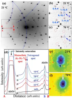
Figures1共a兲–1共c兲show the temperature dependence of the micro-x-ray diffraction patterns for a VO2 film. Spots in the patterns are due to planes diffracted from the 3⫻2.5 m2 area on VO2/Al2O3 by the focused polychromatic micro-x-ray beam. The strong Laue spots in Fig.1共a兲are those of the substrate, while the weak Laue spots denoted by red circles in the guided box are from the VO2 film. For close exami-nation of the weak Laue spots, the image in the box of Fig. 1共a兲is enlarged and sharpened by image processing tools, as shown in Fig. 1共b兲. Five Laue spots indicated by red-dot circles are planes corresponding to the monoclinic structure in VO2; the plane indices are written in the figure. These weak M Laue spots disappear at 70 ° C leaving only the center spot, as shown in Fig.1共c兲. A plane index of the center spot at 70 ° C is not determined using only one spot in the simulation program, but the center spot is regarded as a plane in the tetragonal structure on the basis of previous measurements.12,22,24
In order to observe whether there is the shift of the center spots in the M and R structures, we scanned the position of the spots from A to B in the box of Fig.1共a兲with tempera-ture, as shown in Fig.1共d兲. Reference Al2O3spots indicated by mark S in Fig.1共d兲do not move with temperature. A new peak in the tetragonal structure appears at a position slightly shifted to the right from 共6 , −10, −7兲 the M peak. Spot im-ages indicating the different positions of the center spots are shown in Figs.1共e兲and1共f兲. Thus, the disappearance of the five diffraction spots and the emergence of one strong spot in the center indicate that VO2underwent a SPT from the M to the tetragonal structure.
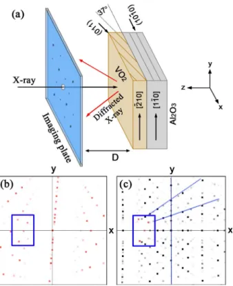
The above Laue spot indices and information on the struc-tural alignment in VO2/Al2O3 were obtained by analyzing the data with a simulation program.29 In the real configura-tion of the measurement, the polychromatic x-ray beam along the –zdirection was focused on the tilted sample plane and the Laue patterns were collected with the CCD camera. In the simulation program, a back-reflection method was se-lected and the simulation parameters in the Fig.2共b兲caption were determined to have the same Laue pattern关Fig. 1共a兲兴. Figure 2共a兲shows a diagram of the structure resulting from the simulation configuration with the crystal alignment infor-mation. The VO2 film deposited on the 共1010兲 Al2O3 sub-strate has a tilted 共011兲 plane of 37° to the substrate plane. The normal crystal directions共ydirection兲of VO2and Al2O3 to the incident x ray are关¯210兴and关11¯0兴, respectively. Figure 2共b兲shows the Laue pattern simulated by using these param-eters in VO2. Figure2共c兲exhibits that the boxed area in Fig.
FIG. 1. 共Color online兲 共a兲Laue spots measured at 21 ° C by a micro-x-ray beam. Strong spots are from the 共101¯0兲 Al2O3 sub-strate, and the weak spots in the box come from the VO2film.共b兲
An enlarged image of the box in Fig.1共a兲. VO2spots circled by red dots are indexed. The reference Al2O3spot is denoted byS.共c兲An
enlarged image of the VO2 spot measured at 70 ° C.共d兲 Scanned
intensity taken from A to B in the box of Fig.1共a兲. A strong spot near A is one of the substrate spots and a weak spot near B is one of the center spots coming from the VO2 film. The reference Al2O3 spots do not move with temperature. 共e兲 Enlarged image of the center spot,共6 , −10, −7兲, in the monoclinic structure at 21 ° C.共f兲 Enlarged image of the center spot in the tetragonal structure at 70 ° C. The position difference between two center spots is shown in Figs.1共e兲and1共f兲.
2共b兲overlaps the simulated Al2O3 Laue pattern at the same position. This area is included into the boxed area in Fig. 1共a兲.
Figure 3 shows theI-V curve observed for revealing the relation between the MIT and the SPT for the VO2-based two-terminal device installed in the x-ray diffraction hutch. The MIT voltage is approximately 4.2 V. The ohmic behav-ior, corresponding to the characteristic of a metal, is ob-served above 4.2 V. This indicates that the VO2film became a metal. Furthermore, the current jump near 4.2 V was ex-plained by the divergence in the hole-driven MIT theory关 ex-tended Brinkman-Rice1,6,30 共BR兲 picture兴 and the BR picture.7
The image in the inset of Fig. 3, taken after finishing measurements, shows a device consisting of the etched VO2 film on which the x-ray beam of 3⫻2.5 m2 was focused and exhibits black marks on both electrode sides. The black marks translate to residual photoresist 共used for the lift-off process of a metal electrode兲burned by high currents after the jump, and their shapes are uniform to the cross-sectional direction. This indicates that current uniformly flowed in the channel width. The maximum current during the experiment was as high as 25 mA. The device reproduced similar I-V
characteristic curves to those obtained even after finishing x-ray diffraction experiments.
For the structural analysis of VO2, eachI-Vmeasurement and the micro-x-ray experiment were simultaneously per-formed at each voltage. Laue patterns were obtained at sev-eral voltages. These measurement points are denoted by ar-rows in Fig. 3. During the measurement of each Laue pattern, a constant current was sustained.
Figures4共a兲–4共f兲show the voltage dependence of micro-x-ray diffraction patterns measured for the device at room temperature. The micro-x-ray experiments were carried out at the voltage values indicated by the arrows in Fig. 3. The substrate Laue patterns are slightly different from that in Fig. 1共a兲because of the difference of the experimental configura-tion. Five clear M VO2 spots are shown from 0 to 5 V in Figs. 4共a兲–4共c兲. At 7 and 8 V, the four spots excluding the central spot become very weak. At 10 V, only the center spot is very clear 关Fig. 4共f兲兴. These results indicate that the M structure begins to change to the R structure from 8 V. The VO2film has the M structure up to 7 V, although the MIT at 4.2 V has already occurred 共Fig.3兲.
Figure4共g兲shows the intensity changes of five spots with increasing voltage. The remarkable decrease in the intensity of the P1, P2, P3, P4, and M spots are not observed up to 7 V. At 8 V and higher, the intensity of the M spot slightly increases because a new T spot appears, while other spots abruptly drop to zero. The intensities of the substrate spots
FIG. 2.共a兲 共Color online兲A schematic diagram of the simulation configuration of x-ray microdiffraction.共b兲A computer-calculated Laue pattern of a tilted共011兲VO2plane with a 37° slope along the
xaxis. The vertical y direction is关2¯10兴. Spots in the blue boxed area are similar to those in the box of Fig.1共a兲. The simulation param-eters of VO2, a= 5.7520 Å, b= 4.5380 Å, and c= 5.3830 Å, a
monoclinic angle of = 122.60°, and space group P121/c 1共14兲 -monoclinic were used. 共c兲 A computer-calculated Laue pattern of the共101¯0兲Al2O3substrate with a关11¯0兴vertical direction to they
axis. The only blue boxed area in共b兲overlaps the simulated Al2O3
Laue pattern to compare with the true image of Fig.1共a兲.
FIG. 3.共Color online兲Inset: A microsurface image of the device with a length of 10 m and a width of 3 m after finishing ex-periments. The micro-x-ray beam was focused on the center of the VO2film. The uniform black marks to the cross-sectional direction at both electrode sides translate to burned photoresists by high cur-rents; this is evidence of the absence of the current path 共 break-down兲. I-V sweeps for the device were simultaneously measured with micro-x-ray diffraction experiments. VMITis 4.2 V at the jump.
The micro-x-ray measurements were carried out at voltages of 0, 4, 5, 7, 8, and 10 V.
remained relatively constant. This indicates that the domi-nant structural change occurs between 7 and 8 V.
We can assume a structural inhomogeneity with both the M structure of a low temperature semiconducting phase and the R structure of a high-temperature metallic phase between 5 and 7 V. In this case, five Laue spots would be observed because the R structure has only one spot near 共6 , −10, −7兲.
Therefore, it is very important to find the positional differ-ence between the center spots. A position near the center spot was scanned关Fig.4共h兲兴, and the scan data show broad peaks including the tetragonal center spot at 8 and 10 V. Splitting of the two spots is not obvious, and this can be attributed to background noise shown with blue color in Figs. 4共i兲–4共l兲. The magnified spot images at 0, 5, and 7 V in Figs.4共i兲–4共k兲 exhibit only the M center spot of共6 , −10, −7兲. The spot im-age at 8 V in Fig. 4共l兲displays the R tetragonal center spot, which is caused by a temperature increase induced by joule heating due to the high current; the temperature will be equal to or larger than TSPT. This indicates that the metal phase in the VO2film has only an M structure between 4 and 7 V. The metallic phase from 4 to 7 V is regarded as the monoclinic metal 共MM兲phase共region II in Fig.3兲.
The MM phase can be also regarded as the monoclinic and correlated metal 共MCM兲 phase as evidence of the Mott MIT;20,30 the presence of the correlation in the MM phase was deduced by the spectroscopic method in a previous paper.19The Mott MIT can be viewed as a transition between the M2 antiferromagnetic insulator phase4 and the MCM phase.
The MIT between the M insulator phase and the MM phase observed here differs from the MIT between the M2 insulator phase and the R metal phase4,8and is also distinct from the MIT between the M1 insulator phase and the R metal phase, as observed by many authors.5,9,11–13 The ab-sence of a strong correlation in the R metal phase was shown in the inset of Fig. 3共d兲in Ref.19.
IV. CONCLUSION
In conclusion, by observing the monoclinic and metal phase between the MIT and the SPT using a focused poly-chromatic synchrotron micro-x-ray beam, it is interpreted that VO2 is a Mott insulator undergoing the first-order Mott MIT prior to SPT.
ACKNOWLEDGMENTS
We acknowledge D. N. Basov and M. M. Qazilbash for their valuable comments. This research was supported by the High-Risk High Return projects at ETRI.
1H. T. Kim, B. G. Chae, D. H. Youn, S. L. Maeng, G. Kim, K. Y.
Kang, and Y. S. Lim, New J. Phys. 6, 52共2004兲.
2J. S. Lee, M. Ortolani, U. Schade, Y. J. Chang, and T. W. Noh,
Appl. Phys. Lett. 91, 133509共2007兲.
3M. Fiebig, K. Miyano, Y. Tomioka, and Y. Tokura, Science 280,
1925共1998兲.
4T. M. Rice, H. Launois, and J. P. Pouget, Phys. Rev. Lett. 73,
3042共1994兲.
5R. M. Wentzcovitch, W. W. Schulz, and P. B. Allen, Phys. Rev.
Lett. 72, 3389共1994兲.
6H. T. Kim, Physica C 341-348, 259共2002兲; H. T. Kim, New
Trends in Superconductivity, NATO Science Series, II/67共 Klu-wer, Dordrecht, 2002兲, p. 137.
7W. F. Brinkman and T. M. Rice, Phys. Rev. B 2, 4302共1970兲. 8J. P. Pouget, H. Launois, J. P. D’Haenens, P. Merender, and T. M.
Rice, Phys. Rev. Lett. 35, 873共1975兲.
9J. B. Goodenough, J. Solid State Chem. 5, 145共1972兲. 10J. B. Boyce, F. G. Bridges, T. Claeson, T. H. Geballe, G. G. Li,
and A. W. Sleight, Phys. Rev. B 44, 6961共1991兲.
11M. W. Haverkort, Z. Hu, A. Tanaka, W. Reichelt, S. V. Streltsov,
M. A. Korotin, V. I. Anisimov, H. H. Hsieh, H. J. Lin, C. T. Chen, D. I. Khomskii, and L. H. Tjeng, Phys. Rev. Lett. 95, FIG. 4. 共Color online兲 Voltage dependence of Laue patterns
measured at voltage values denoted in Fig.3. In共a兲–共f兲, the strong Laue spots arise from the Al2O3 substrate, and weak spots come from the VO2film.共g兲Intensity changes of P1, P2, P3, P4, M, and
T spots denoted in共a兲–共f兲with increasing voltage to constant inten-sity of substrate spots.共h兲A scanned image through the center spots from A to B as indicated in 共a兲. 共i兲–共l兲 Enlarged images near the center spots.共k兲and共l兲show the positional difference between the center spots.
196404共2005兲.
12A. Cavalleri, Cs. Toth, C. W. Siders, J. A. Squier, F. Raksi, P.
Forget, and J. C. Kieffer, Phys. Rev. Lett. 87, 237401共2001兲.
13M. Nakajima, N. Takubo, Z. Hiroi, Y. Ueda, and T. Suemoto,
Appl. Phys. Lett. 92, 011907共2008兲.
14S. Biermann, A. Poteryaev, A. I. Lichtenstein, and A. Georges,
Phys. Rev. Lett. 94, 026404共2005兲.
15K. Okazaki, H. Wadati, A. Fujimori, M. Onoda, Y. Muraoka, and
Z. Hiroi, Phys. Rev. B 69, 165104共2004兲.
16C. Kübler, H. Ehrke, R. Huber, R. Lopez, A. Halabica, R. F.
Haglund, Jr., and A. Leitenstorfer, Phys. Rev. Lett. 99, 116401 共2007兲.
17R. Eguchi, M. Taguchi, M. Matsunami, K. Horiba, K.
Yama-moto, Y. Ishida, A. Chainani, Y. Takata, M. Yabashi, D. Miwa, Y. Nishino, T. Tamasaku, T. Ishikawa, Y. Senba, H. Ohashi, Y. Muraoka, Z. Hiroi, and S. Shin, arXiv:cond-mat/0607712 共 un-published兲.
18M. Gatti, F. Bruneval, V. Olevano, and L. Reining, Phys. Rev.
Lett. 99, 266402共2007兲.
19M. M. Qazilbash, M. Brehm, B. G. Chae, P. C. Ho, G. O.
An-dreev, B. J. Kim, S. J. Yun, A. V. Balatsky, M. B. Maple, F. Keilmann, H. T. Kim, and D. N. Bosov, Science 318, 1750 共2007兲.
20H. T. Kim, Y. W. Lee, B. J. Kim, B. G. Chae, S. J. Yun, K. Y.
Kang, K. J. Han, K. J. Yee, and Y. S. Lim, Phys. Rev. Lett. 97, 266401共2006兲.
21E. Arcangeletti, L. Baldassarre, D. Di Castro, S. Lupi, L.
Mala-vasi, C. Marini, A. Perucchi, and P. Postorino, Phys. Rev. Lett.
98, 196406共2007兲.
22B. J. Kim, Y. W. Lee, B. G. Chae, S. J. Yun, S. Y. Oh, H. T. Kim,
and Y. S. Lim, Appl. Phys. Lett. 90, 023515共2007兲.
23M. S. Grinolds, V. A. Lobastov, J. Weissenrieder, and A. H.
Zewail, Proc. Natl. Acad. Sci. U.S.A. 103, 18427共2006兲.
24P. Baum, D. S. Yang, and A. H. Zewail, Science 318, 788
共2007兲.
25H. S. Choi, J. S. Ahn, J. H. Jung, T. W. Noh, and D. H. Kim,
Phys. Rev. B 54, 4621共1996兲.
26Y. J. Chang, J. S. Yang, Y. S. Kim, D. H. Kim, T. W. Noh, D.-W.
Kim, E. Oh, B. Kahng, and J.-S. Chung, Phys. Rev. B 76, 075118共2007兲.
27B. J. Kim, Y. W. Lee, S. Choi, B. G. Chae, and H. T. Kim, J.
Korean Phys. Soc. 50, 653共2007兲.
28J. S. Chung, H. S. Youn, and H. D. Joo, J. Korean Phys. Soc. 44,
256共2004兲.
29Download for free on http://ccp14.sims.nrc.ca/ccp/web-mirrors/
xianrong-huang/.
30H. T. Kim, B. J. Kim, Y. W. Lee, B. G. Chae, and S. J. Yun,