Implementing High-Speed Interfaces with
MachXO2 Devices
Technical Note
FPGA-TN-02153-1.8
Disclaimers
Lattice makes no warranty, representation, or guarantee regarding the accuracy of information contained in this document or the suitability of its products for any particular purpose. All information herein is provided AS IS and with all faults, and all risk associated with such information is entirely with Buyer. Buyer shall not rely on any data and performance specifications or parameters provided herein. Products sold by Lattice have been subject to limited testing and it is the Buyer's responsibility to independently determine the suitability of any products and to test and verify the same. No Lattice products should be used in conjunction with mission- or safety-critical or any other application in which the failure of Lattice’s product could create a situation where personal injury, death, severe property or environmental damage may occur. The information provided in this document is proprietary to Lattice Semiconductor, and Lattice reserves the right to make any changes to the information in this document or to any products at any time without notice.
Contents
1. Introduction ... 6
2. Architecture for High-Speed Interfaces ... 6
2.1. Gearing Logic Distribution ... 6
2.2. Different Types of I/O Logic Cells ... 7
2.3. Clock Domain Transfer at PIO Cells ... 10
3. External High-Speed Interface Description ... 13
4. High-Speed Interface Building Blocks ... 13
4.1. ECLK ... 13 4.2. ECLKSYNC ... 13 4.3. SCLK ... 14 4.4. CLKDIV ... 14 4.5. PLL ... 14 4.6. DQSDLL ... 14 4.7. Input DDR (IDDR) ... 14 4.8. Output DDR (ODDR) ... 14 4.9. Delays ... 15 4.10. DQSBUF ... 15 4.11. IDDRDQS... 15 4.12. ODDRDQS ... 15
5. Generic High-Speed DDR Interfaces ... 16
5.1. High-Speed GDDR Interface Types ... 16
5.2. High-Speed GDDR Interface Details ... 17
5.3. Receive Interfaces ... 17
5.4. Transmit Interfaces ... 24
6. Using IPexpress to Build Generic High-Speed DDR Interfaces ... 30
6.1. Building the SDR Interface ... 31
6.2. Building DDR Generic Interfaces ... 33
6.3. Building a Generic DDR 7:1 Interface ... 36
7. Generic High-Speed DDR Design Guidelines ... 38
7.1. I/O Logic Cells and Gearing Logic ... 38
7.2. High-Speed ECLK Bridge ... 38
7.3. Reset Synchronization Requirement ... 38
7.4. Timing Analysis for High-Speed GDDR Interfaces ... 39
7.5. Timing Rule Check for Clock Domain Transfers ... 43
8. DDR/DDR2/LPDDR SDRAM Interfaces Overview ... 44
9. DDR/DDR2/LPDDR SDRAM Interfaces Implementation ... 46
9.1. DQS Grouping ... 46
9.2. DQS Circuitry ... 46
9.3. I/O Logic Data Path ... 47
9.4. DDR/DDR2/LPDDR Memory READ Implementation ... 47
9.5. DDR/DDR2/LPDDR Memory WRITE Implementation ... 48
10. DDR Memory Interface Generation Using IPexpress ... 51
11. DDR Memory DQ/DQS Design Rules and Guidelines ... 54
12. DDR/DDR2/LPDDR Pinout Guidelines ... 54
13. DDR Software Primitives and Attributes ... 55
13.1. Input DDR Primitives ... 55
13.2. IDDRX2E ... 56
13.3. Output DDR Primitives ... 58
13.4. DDR Control Logic Primitives... 61
Technical Support Assistance ... 67
Figures
Figure 2.1. Basic PIO Cell Supports x1 Gearing Ratio ... 7
Figure 2.2. Memory PIO Cell to Support DDR Memory Applications... 8
Figure 2.3. Video PIO Cell for x2/x4 and 7:1 Applications ... 10
Figure 2.4. 7:1 Deserializer Timing ... 11
Figure 2.5. x2/x4 Deserializer Timing ... 11
Figure 2.6. 7:1 Deserializer Timing in response to ALIGNWD ... 12
Figure 2.7. x2/x4 Deserializer Timing in response to ALIGNWD ... 12
Figure 3.1. External Interface Definition ... 13
Figure 5.1. GIREG_RX Interface... 17
Figure 5.2. GDDRX1_RX.SCLK.Aligned Interface Using DQSDLL ... 18
Figure 5.3. GDDRX1_RX.SCLK.Centered ... 18
Figure 5.4. GDDRX2_RX.ECLK.Aligned Interface ... 19
Figure 5.5. GDDRX2_RX.ECLK.Centered Interface ... 20
Figure 5.6. GDDRX4_RX.ECLK.Aligned Interface ... 21
Figure 5.7. GDDRX4_RX.ECLK.Centered Interface ... 22
Figure 5.8. GDDR71_RX.ECLK.7:1 Interface ... 23
Figure 5.9. GOREG_TX.SCLK Interface ... 24
Figure 5.10. GDDRX1_TX.SCLK.Aligned Interface ... 24
Figure 5.11. GDDRX1_TX.SCLK.Centered Interface ... 25
Figure 5.12. GDDRX2_TX.ECLK.Aligned Interface ... 25
Figure 5.13. GDDRX2_TX.ECLK.Centered Interface ... 26
Figure 5.14. GDDRX4_TX.ECLK.Aligned Interface ... 27
Figure 5.15. GDDRX4_TX.ECLK.Centered Interface ... 28
Figure 5.16. GDDR71_TX.ECLK.7:1 Interface ... 29
Figure 6.1. SDR Interface Selection at the IPexpress Main Window ... 31
Figure 6.2. Configuration Tab for the SDR Interfaces ... 32
Figure 6.3. DDR_Generic Interface Selection at the IPexpress Main Window ... 33
Figure 6.4. Pre-Configuration Tab of the DDR_Generic Interfaces ... 34
Figure 6.5. Configuration Tab of the DDR_Generic Modules ... 35
Figure 6.6. GDDR_71 Interface Selection at the IPexpress Main Window ... 36
Figure 6.7. GDDR_71 Configuration Tab of GDDR_71 ... 37
Figure 7.1. Reset Synchronization for Receive Interfaces ... 39
Figure 7.2. Reset Synchronization for Transmit Interfaces ... 39
Figure 7.3. Receiver RX.CLK.Centered Waveforms ... 40
Figure 7.4. Receiver RX.CLK.Aligned and MEM DDR Input Waveforms ... 40
Figure 7.5. Receiver GDDR71_RX. Waveforms ... 41
Figure 7.6. tCO Minimum and Maximum Timing Analysis ... 41
Figure 7.7. Transmitter TX.CLK.Centered and MEM DDR Output Waveforms ... 42
Figure 7.8. Transmitter TX.CLK.Aligned Waveforms ... 42
Figure 7.9. Transmitter GDDR71_TX. Waveforms ... 43
Figure 8.1. Typical DDR SDRAM Interface ... 44
Figure 8.2. Typical DDR2 SDRAM Interface ... 45
Figure 8.3. Typical LPDDR SDRAM Interface ... 45
Figure 8.4. DQ-DQS Relationship During READ ... 45
Figure 13.2. IDDRX2E Symbol ... 56
Figure 13.3. IDDRX4B Symbol ... 57
Figure 13.4. IDDRX71A Symbol ... 57
Figure 13.5. IDDRXQSX1A Symbol ... 58
Figure 13.6. ODDRXE Symbol ... 58
Figure 13.7. ODDRX2E Symbol ... 58
Figure 13.8. ODDRX4B Symbol ... 59
Figure 13.9. ODDRX71A Symbol ... 59
Figure 13.10. ODDRDQSX1A Symbol ... 60
Figure 13.11. TDDRA Symbol ... 60
Figure 13.12. DQSBUFH Symbol ... 61
Figure 13.13. DQSBUFH Block Diagram ... 62
Figure 13.14. READ Pulse Positioning Optimization ... 63
Figure 13.15. DQSDLLC Symbol ... 63
Figure 13.16. DELAYE Symbol ... 64
Figure 13.17. DELAYD Symbol ... 65
Figure 13.18. DLLDELC Symbol ... 66
Tables
Table 2.1. Gearing Logic Distribution for MachXO2-640U, MachXO2-1200/U and Higher Density Devices ... 6Table 5.1. Generic High-Speed I/O DDR Interfaces ... 16
Table 6.1. Signal Names Used by IPexpress Modules ... 30
Table 6.2. GUI Options for the SDR Interfaces... 32
Table 6.3. GUI Options for the Pre-Configuration Tab of DDR_Generic Modules ... 34
Table 6.4. GUI Options of the Configuration Tab of the DDR_Generic Modules... 35
Table 6.5. Gearing Ratio Selection by the Software ... 36
Table 6.6. GUI Options of the Configuration Tab for GDDR_71 ... 37
Table 7.1. Gearing Logic Supported by Mixed Mode of I/O Logic Cells ... 38
Table 8.1. DDR / DDR2 and LPDDR Specification for MachXO2-640U, MachXO2-1200/U and Higher Density Devices .... 44
Table 10.1. Options of the Configuration Tab of the DDR_MEM Module ... 52
Table 10.2. Options of the Configuration Tab of the DDR_MEM Module ... 53
Table 13.1. MachXO2 DDR Software Primitives ... 55
Table 13.2. TDDRA Attributes ... 60
Table 13.3. DQSBUFH signals ... 61
Table 13.4. DQSDLLC Signals... 63
Table 13.5. Attribute for DQSDLLC ... 64
Table 13.6. DELAYE Signals ... 64
Table 13.7. DELAYE Attributes ... 64
Table 13.8. DEL_MODE Values Corresponding to the GDDR Interface ... 65
Table 13.9. DELAYD signals ... 65
1.
Introduction
In response to the increasing need for higher data bandwidth, the industry has migrated from the traditional Single Data Rate (SDR) to the Double Data Rate (DDR) architecture. SDR uses either the rising edge or the falling edge of the clock signal to transfer data, while DDR uses both edges of the clock signal for data transfer. This essentially doubles the data transmission rate using the same clock frequency because the data is transferred twice per clock cycle. The DDR clocking technique has largely been used in memory interfaces such as DDR SDRAM. As a result, DDR SDRAM memories achieve twice the bandwidth as SDR SDRAM memories without increasing the signal integrity requirements in the system.
The Lattice MachXO2™ PLD family supports high-speed interfaces for both DDR and SDR applications through built-in Programmable I/O (PIO) logic. The MachXO2 devices also have dedicated circuitry to support DDR, DDR2, and LPDDR SDRAM memory interfaces. This document focuses on the implementation of high-speed generic DDR interfaces, and memory DDR/DDR2 and LPDDR interfaces in the MachXO2 devices. It also provides guidelines for making use of the built-in capabilities of the MachXO2 devices to achieve the best performance for highspeed interfaces.
2.
Architecture for High-Speed Interfaces
2.1.
Gearing Logic Distribution
The high-speed generic DDR (GDDR) interfaces are supported through the built-in gearing logic in the Programmable I/O (PIO) cells. This gearing is necessary to support high-speed I/O while reducing the performance requirement on the FPGA fabric.
There are four gearing ratio settings available in the MachXO2 devices depending on the I/O bank locations and the logic density. The x1 gearing ratio is available in all banks for all the device densities. The x2, x4, and the 7:1 gearing ratio are available in the top and bottom banks of the MachXO2-640U, MachXO2-1200/U and higher density devices. The 7:1 gearing ratio is mainly used for video display applications. The x2/x4 gearing circuit is shared with the 7:1 circuit on both receive and the transmit sides. The right bank of the MachXO2-640U, MachXO2-1200/U and higher density devices support the memory DDR interface. The memory DDR uses x1 gearing logic in the dedicated memory PIO cells. Table 2.1. gives a breakdown of gearing logic support in the different I/O banks. Details of PIO cells can be found in the MachXO2 Family Data Sheet (FPGA-DS-02056).
Table 2.1. Gearing Logic Distribution for MachXO2-640U, MachXO2-1200/U and Higher Density Devices
Gearing Logic Definition Gearing Ratio Left Right Bottom Top
DDR x1* GDDR 1:2 or 2:1 Yes Yes Yes Yes
Input DDR x2 GDDR 1:4 — — Yes — Input DDR x4 GDDR 1:8 — — Yes — Input DDR 7:1 GDDR 1:7 — — Yes — Output DDR x2 GDDR 4:1 — — — Yes Output DDR x4 GDDR 8:1 — — — Yes Output DDR 7:1 GDDR 7:1 — — — Yes
mem DDR x1 Memory DDR 1:2 or 2:1 — Yes — —
2.2.
Different Types of I/O Logic Cells
In order to support various gearing ratios, the MachXO2 devices support three types of PIO logic cells. These include a basic PIO cell, a memory PIO cell, and a video PIO cell.
The basic PIO cell supports traditional SDR registers and DDR x1 registers. It is available on all sides of all MachXO2 devices. The memory PIO cell supports DDR memory applications and is available on the right side of the MachXO2-640U, MachXO2-1200/U and higher density devices. The video PIO cell supports the x2/x4 and 7:1 gearing applications. They are available on MachXO2-640U, MachXO2-1200/U and larger devices on the bottom side for the receive
interfaces, and on the top side for the transmit interfaces. The input and output structures of each type of PIO cell are discussed in detail in the MachXO2 Family Data Sheet (FPGA-DS-02056). The block diagrams of the PIO cells are shown here again in this document for reference.
Output Path Input Path TQ D/LQ TD Tri-state Path Q D1 D Q D Q Q1 D/LQ Q0 D0 SCLK SCLK INCK Q1 Q0 INDD D Q0 Q1 D Q Programmabl e Del ay Cell D Q D/LQ D Q
Output Path Input Path TQ D/LQ TD Tri-state Path Q D1 D Q D Q Q1 D/LQ Q0 D0 SCLK SCLK INCK Q1 Q0 INDD D Q0 Q1 D Q Programmabl e Del ay Cell D Q D/LQ D Q
D Q D ECLK0/1 SCLK Q21 Q0_ S2 S0 D Q D Q T2 T0 Q0 Q2 D Q D Q CE D Q CE D Q Q65 Q43 S6 S4 D Q D Q T6 T4 D Q cdn D Q CE D Q cdn CE D Q Q54 Q_6 S3 S5 D D T3 T5 Q6 D Q D Q CE D Q CE D Q Q10 Q32 S1 D T1 D Q D Q CE Q65 Q65 Q43 Q43 Q21 Q10 Q21 Q32 Q54 Q_6 Q54 Q32 SEL0 Q4 Q5 Q1 Q3 S7 D Q T7 D Q CE Q7 UPDATE Q_6 8-bit rx_data from x4 gearing 4-bit rx_data from x2 gearing Not used in 1:7 de-serialization IDDRx2_A IDDRx2_C IDDRx2_C Receive Path Programmable Delay Cell
GND Not used in 7:1 Serialization 8-Bit tx_data from x4 Gearing 4-Bit tx_data from x2 Gearing Transmit Path
Figure 2.3. Video PIO Cell for x2/x4 and 7:1 Applications
2.3.
Clock Domain Transfer at PIO Cells
The MachXO2 gearing logic performs serializing and de-serializing of high-speed data in the PIO cells. The clock domain transfer for the data from the high-speed edge clock (ECLK) to the low-speed system clock (SCLK) is guaranteed by design through two internal signals, UPDATE and SEL. The SEL signal toggles between ‘0’ and ‘1’ to sample three bits or four bits of data at a time for the 7:1 gearing. It remains static during the x2/x4 gearings. The UPDATE signal behaves the same for all the gearings to update the register with the correct byte of data. This data is then clocked by the SCLK for downstream processing. Figure 2.3. illustrates the architecture of x2 /x4 input gearing logic.
MachXO2 devices provide logic to support word alignment with minimal FPGA resources. The word alignment results in a shift to the UPDATE, SEL and the SCLK signals. It can be activated by providing an alignment request signal to the ALIGNWD port of the high-speed interface components. ALIGNWD can be asynchronous to the ECLK domain, but it
Figure 2.4. and Figure 2.5. provide a timing relationship of UPDATE, SEL, ECLK, and SCLK signals under different gearing requirements Figure 2.6. and Figure 2.7. show the word alignment procedure for various gearing ratios. The discussion of gearing logic is applicable to both receive and transmit sides of the high-speed interfaces. Refer to reference design
MachXO2, MachXO3 and ECP5 7:1 LVDS Video Interface (FPGA-RD-02093), for more details on implementing word
alignment using the 7:1 gearing function.
The clock domain transfer for the DDR memory interface is accomplished by using the built-in, 90°-shifted clock trees for memory READ and WRITE operations. DLL and DQS detection logic are provided to guarantee the correct receive and transmit of data to and from DDR memories.
0 e 1 e 2 e 3 e 4 e 5 e 6 e 0 c 1 c 2 c 3 c 4 c 5 c 6 c 0 a 1 a 2 a 3 a 4 a 5 a 6 a d6d5d4d3d2d1d0 D ECLK UPDATE SEL SCLK Q(6:0) c4 c5 c6 d0 d1 d2 d3 d4 d5 d6 e0 e1 e2 e3 e4 e5 e6 e7 f0 f1 f2 f3 f4 f5 f6 g0 g1 g2
Figure 2.4. 7:1 Deserializer Timing
2 e 3 e 4 e 5 e 6 e 7 e 0 c 1 c 2 c 3 c 4 c 5 c 6 c 7 c 0 b 1 b 2 b 3 b 4 b 5 b 6 b 7 b d7d6d5d4d3d2d1d0 D ECLK UPDATE SEL SCLK Q(6:0) c5 c6 c7 d0 d1 d2 d3 d4 d5 d6 d7 e1 e2 e3 e4 e5 e6 e7 f0 f1 f2 f3 f4 f5 f6 f7 g0 g1
5 b 6 b 0 c 1 c 2 c 3 c 4 c 5 a 6 a 0 b 1 b 2 b 3 b 4 b 5 k 6 k 0 a 1 a 2 a 3 a 4 a d6d5d4d3d2d1d0 ALIGNWD Action D ECLK UPDATE SEL SCLK Q(6:0) b2 b3 b4 b5 b6 c0 c1 c2 c3 c4 c5 c6 d0 d1 d2 d3 d4 d5 d6 e0 e1 e2 e3 e4 e5 e6 f0 f1
Figure 2.6. 7:1 Deserializer Timing in response to ALIGNWD
D ECLK c3 7 b 0 c 1 c 2 c 3 c 4 c 5 c 6 c 7 a 0 b 1 b 2 b 3 b 4 b 5 b 6 b d7d6d5d4d3d2d1d0 e7e6e5e4... 0 1 4 f 3 f 2 f 1 f 0 f 7 e 6 e 5 e 4 e 3 e 2 e 1 e 0 e 5 c 4 c c6 c7 d0 d1 d2 d3 d4 d5 d6 d7 UPDATE ALIGNWD Action SEL SCLK Q(6:0)
3.
External High-Speed Interface Description
There are two types of external high-speed interface definitions that can be used with the MachXO2 devices: centered and aligned. In a centered external interface, at the device pins, the clock is centered in the data opening. In an aligned external interface, the clock and data transition are aligned at the device pins. This is sometimes called “edge-on-edge”.
Figure 3.1. shows external interface waveforms for SDR and DDR. At the receive side, an aligned interface requires clock delay adjustment to position the clock edge at the middle of the data opening to ensure that the capture flip-flop setup and hold times are not violated. Similarly a centered interface at the transmit side will require a clock delay adjustment to position the clock at the center of the data opening for transmission.
Note that centered and aligned interfaces might both be used for a given bus. For example, in a DDR SDRAM memory the clock and data relationship during READ is an aligned interface, while the clock and data relationship during WRITE is a centered interface. Clock at pin d e r e t n e C R D S d e n g il A R D S d e r e t n e C R D D d e n g il A R D D Data at pin Clock at pin Data at pin
Figure 3.1. External Interface Definition
4.
High-Speed Interface Building Blocks
MachXO2 devices provide dedicated logic blocks for building high-speed interfaces, with each block performing a unique function. Combining various blocks gives ultimate performance of a specific interface. The hardware
components in the device are described in this section. The DDR Software Primitives and Attributes section describes the library elements for these components. Refer to MachXO2 sysCLOCK PLL Design and Usage Guide (FPGA-TN-02157), for an in-depth discussion of clocking and PLL architectures.
4.1.
ECLK
Edge clocks are high-speed, low-skew I/O dedicated clocks. Two edge clocks (ECLK) are available on each of the top and bottom sides for MachXO2-640U, MachXO2-1200/U and higher density devices. The primary clock nets (PCLK) have direct connectivity to ECLKs. The bottom PCLK pins also have minimal routing to PLLs for video applications.
4.2.
ECLKSYNC
This is the ECLK synchronization block. Each ECLK has its own ECLKCYNC component to synchronize the clock domain transfer of data. This block can also be used to dynamically disable an edge clock to save power during operation.
4.3.
SCLK
SCLK refers to the system clock of the design. SCLK must use primary clock pins or primary clock nets for high speed interfaces. There are eight primary clock pins (PCLK) available for the MachXO2 device, and eight primary clock nets in the MachXO2 devices.
4.4.
CLKDIV
Clock dividers are used to generate low-speed system clocks from a high-speed edge clock. There are two clock dividers per top and bottom sides of the MachXO2-640U, MachXO2-1200/U and higher density devices. The ECLK frequency can be divided down by 2, by 3.5, or by 4 through the CLKDIV component.
4.5.
PLL
A maximum of two PLLs are available in the MachXO2 devices. The number of PLLs varies with the logic density. The MachXO2-640U, MachXO2-1200/U and MachXO2-2000 have one PLL. MachXO2-2000U, MachXO2-4000, and MachXO2-7000 devices have two PLLs. There are pre-assigned dual-purpose I/O pins that drive to PLLs as reference clock inputs.
4.6.
DQSDLL
A maximum of two DQSDLLs are available in the MachXO2-640U, MachXO2-1200/U and higher density devices. The top-right DQSDLL controls the top and right banks. The bottom-left DQSDLL can be used by the bottom and left banks. This component can be used for both DDR memory and generic high-speed interfaces. The DQSDLL, together with the clock slave delay cell (DLLDEL), is used to create a 90° clock shift/delay for aligned receiver interfaces.
4.7.
Input DDR (IDDR)
Generic input DDR components support x1, x2, x4, and 7:1 gearing ratios at the receiving side of the PIO cells. The x1 gearing is supported by IDDRX, or the basic PIO cell. It receives 1-bit DDR data and outputs 2-bit wide parallel data synchronized to the SCLK. There is no clock domain transfer involved in the x1 gearing. The x2 gearing is supported by IDDRX2. It receives 1-bit DDR data synchronized to the ECLK and outputs four bits of parallel data synchronized to the SCLK. The same function applies to the IDDRX4, which receives a single bit of DDR data synchronized to the ECLK and outputs eight bits of parallel data synchronized to the SCLK. The 7:1 gearing shares the same structure as the x4 gearing. The 7:1 gearing outputs seven bits of parallel data instead of eight. The generic high-speed interface gearings are supported by the video PIO cells.
4.8.
Output DDR (ODDR)
Generic output DDR components support x1, x2, x4, and 7:1 gearing ratios at the transmit side of the PIO cells. The x1 gearing is supported by ODDRX, or the basic PIO cell. It serializes the 2-bit data based on SCLK. There is no clock domain transfer involved in x1 gearing. The x2 gearing is supported by ODDRX2. The 4-bit parallel data is clocked by SCLK and is serialized using ECLK. The x4 gearing is supported by ODDRX4. The 8-bit parallel data is clocked by SCLK and is serialized using ECLK. The 7:1 gearing shares the same structure as the x4 gearing. The 7-bit parallel data is serialized by the ECLK. The generic high speed interface gearings are supported by the video PIO cells.
4.9.
Delays
There are two types of delay available for high-speed interfaces. The first type is the I/O logic delay that can be applied on the input data paths, as shown in the block diagram of PIO architectures at the beginning of the document.
Although the 32-tap I/O logic delay can be static or dynamic, only the bottom side of the 640U, MachXO2-1200/U and higher density devices supports dynamic data path delay. The static I/O logic delay (DELAYE) is used by default when configuring the interface in the Lattice design software. Software applies fixed delay values based on the interface used. Dynamic delay (DELAYD) at the bottom-side input data path provides dynamic or user-defined delay. Dynamic delay requires extra ports available on the module to be connected to user logic for delay control. The I/O logic delay is used to achieve the SDR zero hold timing, or match primary clock injection for x1 gearing, or match the edge clock injection for x2/x4 gearings.
The second type of delay is the clock slave delay cell (DLLDEL), which delays the incoming clock by 90° to place the clock in the middle of the data opening. This block is digitally controlled by the DQSDLL through 7-bit control code. There is one clock slave delay cell per primary clock pin. Its input comes from the primary clock pins and its output can drive the primary clock net for the x1 aligned interface or ECLK for x2/x4 aligned interfaces.
4.10.
DQSBUF
This is the dedicated DQS circuitry for DDR memory. It generates a 90° shift on DQS for memory read operations, and a 90° shift on the SCLK for memory write operations. The clock polarity detection, burst detection, and data valid signals are generated from this block. This is available on the right bank of the MachXO2-640U, MachXO2- 1200/U and higher density devices.
4.11.
IDDRDQS
DDR memory input buffer supports clock domain transfers from DQS to SCLK. These memory PIO cells are used exclusively for DDR memory interfaces and are used for DDR memory READ operations. They are available on the right bank of the MachXO2-640U, MachXO2-1200/U and higher density devices.
4.12.
ODDRDQS
The DDR memory output buffer supports clock domain transfers from SCLK to DQS. These memory PIO cells are used exclusively for DDR memory interfaces and are used for DDR memory WRITE operations. They are available on the right bank of the MachXO2-1200 and higher density devices.
5.
Generic High-Speed DDR Interfaces
Generic high-speed interfaces, or Generic DDR (GDDR), are supported in MachXO2 using the dedicated logic blocks. This section will discuss the GDDR types, the interface logic, and the software to support the GDDR capability in the silicon.
5.1.
High-Speed GDDR Interface Types
The GDDR interfaces supported by the MachXO2 device family are pre-defined in the software and characterized in the silicon. Table 5.1. lists all the supported interfaces and gives a brief description of each interface.
Table 5.1. Generic High-Speed I/O DDR Interfaces
Mode Interface Name Description Supporting Device & Sides
RX SDR GIREG_RX.SCLK SDR input using SCLK All devices, all sides
RX GDDRx1 Aligned GDDRX1_RX.SCLK.Aligned DDRx1 input using SCLK, data is
edge-to-edge with incoming clock
640U, 1200/U, and above, all sides
RX GDDRx1 Centered GDDRX1_RX.SCLK.Centered DDRx1 input using SCLK, incoming
clock is centered at the data opening
All devices, all sides
RX GDDRx2 Aligned GDDRX2_RX.ECLK.Aligned DDRx2 input using ECLK, data is
edge-to-edge with incoming clock
640U, 1200/U, and above, bottom
RX GDDRx2 Centered GDDRX2_RX.ECLK.Centered DDRx2 input using ECLK, incoming
clock is centered at the data opening
640U, 1200/U, and above, bottom
RX GDDRx4 Aligned GDDRX4_RX.ECLK.Aligned DDRx4 input using ECLK, data is
edge-to-edge with incoming clock
640U, 1200/U, and above, bottom
RX GDDRx4 Centered GDDRX4_RX.ECLK.Centered DDRx4 input using ECLK, incoming
clock is centered at the data opening
640U, 1200/U, and above, bottom
RX GDDR71 GDDR71_RX.ECLK.7:1 GDDR 7:1 input using ECLK 640U, 1200/U, and above,
bottom
TX SDR GOREG_TX.SCLK SDR output using SCLK All devices, all sides
TX GDDRx1 Aligned GDDRX1_TX.SCLK.Aligned DDRx1 output using SCLK, data is
edge-to-edge with outgoing clock
All devices, all sides
TX GDDRx1 Centered GDDRX1_TX.SCLK.Centered DDRx1 output using SCLK, outgoing
clock is centered at the data opening
640U, 1200/U, and above, all sides
TX GDDRx2 Aligned GDDRX2_TX.ECLK.Aligned DDRx2 output using ECLK, data is
edge-to-edge with outgoing clock
640U, 1200/U, and above, top
TX GDDRx2 Centered GDDRX2_TX.ECLK.Centered DDRx2 output using ECLK, outgoing
clock is centered at the data opening
640U, 1200/U, and above, top
TX GDDRx4 Aligned GDDRX4_TX.ECLK.Aligned DDRx4 output using ECLK, data is
edge-to-edge with outgoing clock
640U, 1200/U, and above, top
TX GDDRx4 Centered GDDRX4_TX.ECLK.Centered DDRx4 output using ECLK, outgoing
clock is centered at the data opening
640U, 1200/U, and above, top
TX GDDR71 GDDR71_TX.ECLK.7:1 GDDR 7:1 output using ECLK 640U, 1200/U, and above, top
Notes:
For the “R1” version of the MachXO2 devices GDDRX2, GDDRX4 and GDDR71 modes, ECLKSYNC may have a glitch in the output under certain conditions, leading to possible loss of synchronization. The “R1” versions of the MachXO2 devices have an “R1” suffix at the end of the part number (e.g., LCMXO2-1200ZE-1TG144CR1). For more details on the R1 to Standard migration refer to Designing for Migration from MachXO2-1200-R1 to Standard (Non-R1) Devices (FPGA-AN-02012).
The following describes the naming conventions used for each of the interfaces listed in Table 5.1. G – Generic
IREG – SDR input I/O register
OREG – SDR output I/O register
DDRX1 – DDR x1 I/O register DDRX2 – DDR x2 I/O register DDRX4 – DDR x4 I/O register DDR71 – DDR 7:1 I/I register _RX – Receive interface _TX – Transmit interface
ECLK – Uses ECLK (edge clock) clocking resource at the GDDR interface
SCLK – Uses SCLK (primary clock) clocking resource at the GDDR interface
Centered – Clock is centered to the data when coming into the device
Aligned – Clock is aligned edge-on-edge to the data when coming into the device
5.2.
High-Speed GDDR Interface Details
This section describes each of the generic high-speed interfaces in detail including the clocking to be used for each interface. For detailed information about the MachXO2 clocking structure, refer to MachXO2 sysCLOCK PLL Design and Usage Guide (FPGA-TN-02157). As listed in Table 5.1., each interface is supported in specific bank locations of the MachXO2 devices. It is important to follow the architecture and various interface rules and preferences listed under each interface in order to build these interfaces successfully. The discussion of each component can be found in the DDR Software Primitives and Attributes section of this document.
5.3.
Receive Interfaces
There are eight receive interfaces pre-defined and supported through Lattice IPexpress™ software. GIREG_RX.SCLK
This is a generic interface for single data rate (SDR) data. The standard I/O register in the basic PIO cell (Figure 2.1.) is used for the implementation. An optional inverter can be used to center the clock for aligned inputs. PLLs or DLLs can be used to remove the clock injection delay or adjust the setup and hold times. There are a limited number of DLLs in the architecture and these should be saved for high-speed interfaces when necessary. This interface can either be built using IPexpress, instantiating an I/O register element, or inferred during synthesis.
Din Din DELAYE IREG IREG CLK CLK Sclk Sclk
Figure 5.1. GIREG_RX Interface
The input data path delay cells can be used on the Din path of the interface. A DELAYE element provides a fixed delay to match the SCLK injection time. The dynamic input delay, DELAYD, is not available for this interface.
Figure 5.1. shows possible implementations of this interface. Interface rules:
GDDRX1_RX.SCLK.Aligned
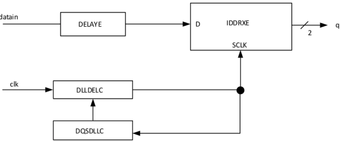
This DDR interface uses the SCLK and the DQSDLL to provide a 90° clock shift to center the clock at the IDDRXE. A DELAYE element is used to adjust data delay for the SCLK clock injection time. The DELAYD is not available for the x1 interface. clk DQSDLLC IDDRXE SCLK D datain DELAYE DLLDELC 2 q
Figure 5.2. GDDRX1_RX.SCLK.Aligned Interface Using DQSDLL Interface rules:
Must use a dedicated clock pin PCLK as the clock source for DLLDELC
A primary clock net must be used to connect DLL outputs to the SCLK port
The DELAYE value should be set to SCLK_ALIGNED for the best timing
There are up to two DQSDLLCs per device. This limits the interface to a maximum of two clock frequencies per device.
GDDRX1_RX.SCLK.Centered
This DDR interface uses DELAYE to match the SCLK delay at the IDDRXE. DELAYD is not available for the x1 interface. Since it is a centered interface, the clock edge is already in the middle of the data opening. There is no logic required to shift the clock.
clk IDDRXE SCLK D datain DELAYE 2 q Figure 5.3. GDDRX1_RX.SCLK.Centered Interface rules:
Must use a dedicated clock pin PCLK as the clock source
DELAYE value should be set to SCLK_CENTERED for the best timing
GDDRX2_RX.ECLK.Aligned
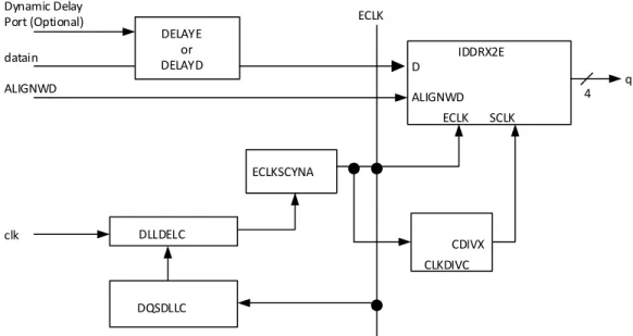
This DDR x2 interface uses the DQSDLL to provide a 90° clock shift to center the clock at the IDDRX2E buffer. DELAYE is used to delay data to match the ECLK injection delay. DELAYD can also be used to control the delay dynamically. This interface uses x2 gearing with the IDDRX2E element. This requires the use of a CLKDIVC to provide the SCLK which is half the frequency of the ECLK. The ECLKSYNCA element is associated with the ECLK and must be used to drive the ECLK. The port ALIGNWD can be used for word alignment at the interface.
DQSDLLC DLLDELC clk ALIGNWD Dynamic Delay Port (Optional) datain ECLKSCYNA ECLK IDDRX2E ECLK SCLK CDIVX CLKDIVC 4 q D ALIGNWD DELAYE or DELAYD
Figure 5.4. GDDRX2_RX.ECLK.Aligned Interface Interface rules:
Must use a dedicated clock pin PCLK as the clock source for DLLDELC
Clock net routed to SCLK must use primary clock net
There are up to two DQSDLLC per device. It limits this interface to a maximum of two clock frequencies per device.
DELAYE should be set to ECLK_ALIGNED
When DELAYD is used, only one dynamic delay port is needed for the entire bus
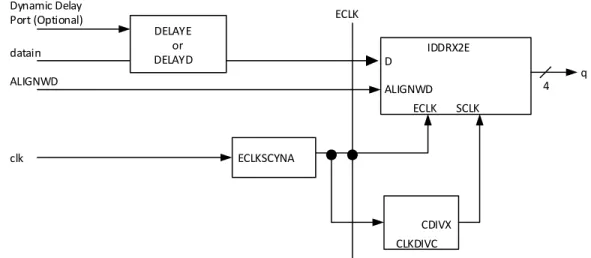
GDDRX2_RX.ECLK.Centered
This DDR x2 interface uses DELAYE or DELAYD to match edge clock delay at the IDDRX2E. Since this interface uses the ECLK it can be extended to support large data bus sizes for the entire side of the device. This interface uses x2 gearing with the IDDRX2D element. This requires the use of a CLKDIVC to provide the SCLK which is half the frequency of the ECLK. The port ALIGNWD can be used for word alignment at the interface.
clk ALIGNWD Dynamic Delay Port (Optional) datain ECLKSCYNA ECLK IDDRX2E ECLK SCLK CDIVX CLKDIVC 4 q D ALIGNWD DELAYE or DELAYD
Figure 5.5. GDDRX2_RX.ECLK.Centered Interface Interface rules:
Must use a dedicated clock pin PCLK as the clock source for ECLKSYNCA
Clock net routed to SCLK must use primary clock net
DELAYE should be set to ECLK_CENTERED
When DELAYD is used, only one dynamic delay port is needed for the entire bus
GDDRX4_RX.ECLK.Aligned
This DDR x4 interface uses the DQSDLL to provide a 90° clock shift to center the edge clock at the IDDRX4B buffer. DELAYE is used to delay data to match the ECLK injection delay. DELAYD can also be used to control the delay
dynamically. Since this interface uses the ECLK, it can be extended to support large data bus sizes for the entire side of the device. This interface uses x4 gearing with the IDDRX4B element. This requires the use of a CLKDIVC to provide the SCLK which is one quarter of the ECLK frequency. ECLKSYNCA element is associated with the ECLK and must be used to drive the ECLK. The port ALIGNWD can be used for word alignment at the interface.
DQSDLLC DLLDELC clk ALIGNWD Dynamic Delay Port (Optional) datain ECLKSCYNA ECLK IDDRX2E ECLK SCLK CDIVX CLKDIVC 8 q D ALIGNWD DELAYE or DELAYD
Figure 5.6. GDDRX4_RX.ECLK.Aligned Interface Interface rules:
Must use a dedicated clock pin PCLK as the clock source for DLLDELC
Clock net routed to SCLK must use primary clock net
There are up to two DQSDLLC per device. It limits this interface to have maximum of two clock frequencies per device.
Data input must use A/B pair of the I/O logic cells for x4 gearing
DELAYE should be set to ECLK_ALIGNED
When DELAYD is used, only one dynamic delay port is needed for the entire bus
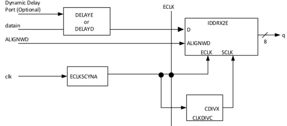
GDDRX4_RX.ECLK.Centered
This DDR x4 interface uses DELAYE or DELAYD to match edge clock delay at the IDDRX4B. Since this interface uses the ECLK it can be extended to support large data bus sizes for the entire side of the device. This interface uses x4 gearing with the IDDRX4B element. This requires the use of a CLKDIVC to provide the SCLK which is one quarter of the ECLK frequency. The port ALIGNWD can be used for word alignment at the interface.
clk ALIGNWD Dynamic Delay Port (Optional) datain ECLKSCYNA ECLK IDDRX2E ECLK SCLK CDIVX CLKDIVC 8 q D ALIGNWD DELAYE or DELAYD
Figure 5.7. GDDRX4_RX.ECLK.Centered Interface Interface rules:
Must use a dedicated clock pin PCLK as the clock source for ECLKSYNCA
Clock net routed to SCLK must use primary clock net
Data input must use A/B pair of the I/O logic for x4 gearing
DELAYE should be set to ECLK_CENTERED
When DELAYD is used, one dynamic delay port is needed for the entire bus
This interface is supported at the bottom side of the MachXO2-640U, MachXO2-1200/U and higher density devices Note: The GDDRX4_RX.ECLK.Centered interface is used to build MIPI D-PHY Receive Interface. Refer to MIPI D-PHY Interface IP (FPGA-RD-02040) for details.
GDDR71_RX.ECLK.7:1
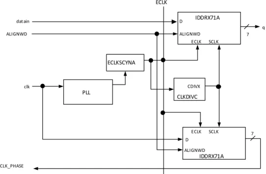
The GDDR 7:1 receive interface is unique among the supported high-speed DDR interfaces. It uses the PLL tosearch the best clock edge to the data opening position during bit alignment process. The PLL steps through the 16 phases to give eight sampling points per data. The data path delay is not used in this interface. CLKDIVC is used to divide down the ECLK by 3.5 due to the nature of the 1:7 deserializing requirement. This means the SCLK is running seven times slower than the incoming data rate. ECLKSYNCA element is associated with the ECLK and must be used to drive the ECLK. The complete 7:1 LVDS video display application requires bit alignment and word alignment blocks to be built in the FPGA resources in addition to the built-in I/O gearing logic and alignment logic. The CLK_PHASE signal is sent to the FPGA side to build the bit alignment logic.
dat ain ALIGNWD clk CLK_PHASE PLL IDDRX71A IDDRX71A CLKDIVC ECLK D D 7 q 7 ALIGNWD ALIGNWD ECLK SCLK ECLK SCLK CDIVX ECLKSCYNA
Figure 5.8. GDDR71_RX.ECLK.7:1 Interface Interface rules:
Must use a dedicated clock pin PCLK at the bottom side as the clock source for PLL
Clock net routed to SCLK must use primary clock net
There are up to two PLLs per device. It limits this interface to have maximum of two clock frequencies per device.
The data input must use A/B pair of the I/O logic cell for 7:1 gearing
5.4.
Transmit Interfaces
There are eight transmit interfaces pre-defined and supported through Lattice IPexpress software. GOREG_TX.SCLK
This is a generic interface for SDR data and a forwarded clock. The standard register in the basic PIO cell is used to implement this interface. The ODDRXE used for the output clock balances the clock path to match the data path. A PLL can also be used to clock the ODDRXE to phase shift the clock to provide a precise clock to data output. There are a limited number of PLLs in the architecture and these should be saved for high-speed interfaces when necessary. This interface can either be built using IPexpress, instantiating an I/O register element, or inferred during synthesis.
OREG ODDRXE SCLK 0 clkout d clk dataout 1
Figure 5.9. GOREG_TX.SCLK Interface Interface rules:
The clock source for SCLK must be routed on a primary clock net GDDRX1_TX.SCLK.Aligned
This output DDR interface provides clock and data that are aligned using a single SCLK. The ODDRXE used for the output clock balances the clock path to match the data path.
clkout d0 d1 clk dataout 1 0 SCLK D0 SCLK D0 D1 D1 ODDRXE ODDRXE
GDDRX1_TX.SCLK.Centered
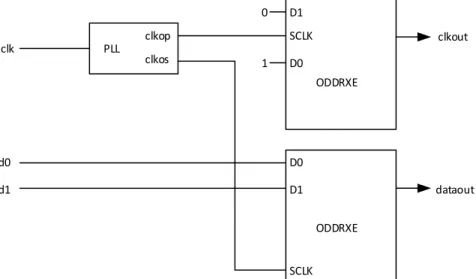
This output DDR interface provides clock and data that are pre-centered. PLL uses clkop and clkos ports to provide the 90° phase difference between the data and the clock. It requires two SCLK resources to drive the output data I/O cell and the output clock I/O cell.
0 1 clkout d0 d1 clk dataout SCLK PLL clkop clkos SCLK D1 D1 D0 D0 ODDRXE ODDRXE
Figure 5.11. GDDRX1_TX.SCLK.Centered Interface Interface rules:
SCLK and 90°-shifted SCLK must be routed on primary clock nets GDDRX2_TX.ECLK.Aligned
This output DDR x2 interface provides clock and data that are aligned. A CLKDIV is used to generate the SCLK which is half of the ECLK frequency. The ECLKSYNC element is used on the ECLK path for data synchronization.
d3 d2 d1 d0 0 1 0 1 clkout clk dataout ODDRX2E ODDRX2E CLKDIV ECLKSYNCA D3 D2 D1 D0 D3 D2 D1 D0 SCLK ECLK SCLK ECLK
Figure 5.12. GDDRX2_TX.ECLK.Aligned Interface Interface rules:
Must use edge clock routing resources for the ECLK
GDDRX2_TX.ECLK.Centered
This output DDR x2 interface provides a clock that is centered at the data opening. The PLL uses clkop and clkos ports to provide the 90° phase difference between the data and the clock. Two ECLK routing resources are used in this interface to drive the output data and the output clock. A CLKDIV is used to generate the SCLK which is half of the ECLK frequency. d3 d2 d1 d0 dataout clkout clk eclk eclk 90° clkop clkos PLL D3 D2 D1 D0 D3 D2 D1 D0 ODDRX2E ODDRX2E SCLK ECLK SCLK ECLK CLKDIV 0 1 0 1 ECLKSYNCA ECLKSYNCA
Figure 5.13. GDDRX2_TX.ECLK.Centered Interface Interface rules:
Must use edge clock routing resources for the ECLK
Since two ECLKs are used on this interface, maximum one bus of this interface can be implemented at a time.
The routing of the SCLK must use primary clock net
GDDRX4_TX.ECLK.Aligned
This output DDR x4 interface provides clock and data that are aligned. A CLKDIV is used to generate the SCLK which is a quarter of the ECLK frequency. The ECLKSYNC element is used on the ECLK path for data synchronization.
d0 d1 d2 d3 d4 d5 d6 d7 dataout clkout clk 1 0 1 0 1 0 1 0 SCLK ECLK SCLK ECLK ODDRX4B ODDRX4B CLKDIV ECLKSYNCA D0 D1 D2 D3 D4 D5 D6 D7 D0 D1 D2 D3 D4 D5 D6 D7
Figure 5.14. GDDRX4_TX.ECLK.Aligned Interface Interface rules:
Must use edge clock routing resources for the ECLK
The routing of SCLK must use primary clock net
Data output must use A/B pair of the I/O logic for x4 gearing
GDDRX4_TX.ECLK.Centered
This output DDR x4 interface provides a clock that is centered at the data opening. The PLL uses clkop and clkos ports to provide the 90° phase difference between the data and the clock. Two ECLK routing resources are used in this interface to drive the output data and the output clock. A CLKDIV is used to generate the SCLK which is one quarter of the ECLK frequency.
dataout clkout clk eclk eclk 90° clkop clkos PLL SCLK ECLK SCLK ECLK CLKDIV ECLKSYNCA ECLKSYNCA ODDRX4B ODDRX4B D3 D2 D1 D0 D7 D6 D5 D4 D3 D2 D1 D0 D7 D6 D5 D4 0 1 0 1 0 1 0 1 d3 d2 d1 d0 d7 d6 d5 d4
Figure 5.15. GDDRX4_TX.ECLK.Centered Interface Interface rules:
Must use edge clock routing resources for the ECLK
Since two ECLKs are used on this interface, a maximum of one bus of this interface can be implemented at a time
The routing of the SCLK must use primary clock net
Data output must use A/B pair of the I/O logic for x4 gearing
This interface is supported at the top side of the MachXO2-640U, MachXO2-1200/U and higher density devices Note: The GDDRX4_TX.ECLK.Centered interface is used to build MIPI D-PHY Transmit Interface. Refer to Refer to MIPI D-PHY Interface IP (FPGA-RD-02040) for details.
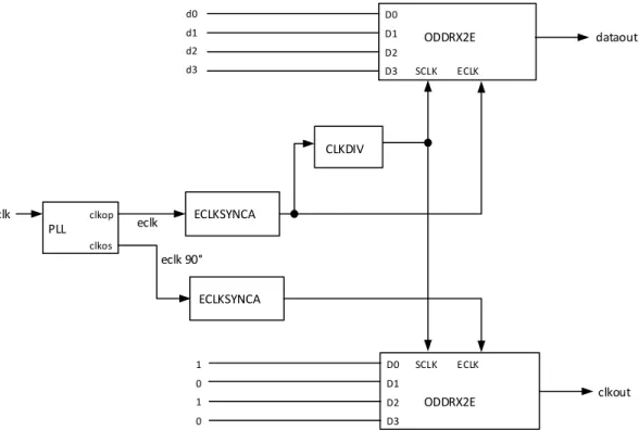
GDDR71_TX.ECLK.7:1
The GDDR 7:1 transmit interface is unique among the supported high-speed DDR interfaces. It uses a specific pattern to generate the output clock, known as pixel clock. The CLKDIVC is used to divide down the ECLK by 3.5 due to the nature of the 7:1 serializing requirement. This means the SCLK is running 7 times slower than the transmit data rate.
ECLKSYNCA element is associated with the ECLK and must be used to drive the ECLK.
dataout clkout clk SCLK ECLK D3 D2 D1 D0 D6 D5 D4 1 1 0 0 0 1 1 ODDRX71A ODDRX71A SCLK ECLK D3 D2 D1 D0 D6 D5 D4 d3 d2 d1 d0 d6 d5 d4 ECLKSYNCA CLKDIV
Figure 5.16. GDDR71_TX.ECLK.7:1 Interface Interface rules:
Must use edge clock routing resources for the ECLK
The routing of SCLK must use primary clock net
Data output must use A/B pair of the I/O logic for 7:1 gearing
6.
Using IPexpress to Build Generic High-Speed DDR Interfaces
The IPexpress tool of the Lattice development software should be used to configure and generate all the generic high-speed interfaces described above. IPexpress will generate a complete HDL module including clocking requirements for each of the interfaces described above. In the IPexpress GUI, all the DDR modules are located under Architecture Modules > IO. This section covers the SDR, DDR_GENERIC, and GDDR_71 interfaces in IPexpress.
Table 6.1. shows the signal names used in the IPexpress modules. Each signal can be used in all or some specified interfaces. The signals are listed separately for the GDDR receive interfaces and the transmit interfaces.
Table 6.1. Signal Names Used by IPexpress Modules
Signal Name Direction Description Supported Interfaces
Receive Interface
clk Input Source synchronous input clock All
reset Input Asynchronous reset to the interface, active high All
datain Input Serial data input at Rx interfaces All
uddcntln Input Hold/update control of delay code, active low. (The
DQSDEL output of DQSDLLC is updated for any PVT variation when UDDCNTLN is held low.)
x1, x2, x4 Aligned
freeze Input Freeze or release DLL, active high. (When high, the device
freezes the DLL to save power while the delay code is preserved. When low, it releases the DLL to resume operation.)
x1, x2, x4 Aligned
alignwd Input Word alignment control signal, active high. (ALIGNWD
can be asynchronous to the ECLK domain, but it must be at least two ECLK cycles wide.)
x2, x4, 7:1
dqsdll_reset Input Asynchronous DQSDLL reset, active high x2, x4 Aligned
clk_s1 Input Slow clock for reset synchronization. (This clock must be
slower than eclk.)
x2, x4, 7:1
init Input Initialize reset synchronization, active high x2, x4, 7:1
phase_dir Input Dynamic Phase adjustment direction. (When 0, phase
shift is delayed by one step. When 1, phase shift is advanced by one step.)
7:1
phase_step Input Dynamic Phase Adjustment Step. (Each step generates a
45-degree shift. PHASESTEP is active low.)
7:1
sclk Output System clock for the FPGA fabric All
q Output Parallel data output of the Rx interfaces All
lock Output DLL or PLL lock x2, x4, 7:1
eclk Output Edge clock generated from the input clock x2, x4 Aligned
rx_ready Output Indicate completion of reset synchronization x2, x4, 7:1
clk_phase Output 7-bit representation of input clock phase. (The clk_phase
is used in the FPGA to build the bit alignment logic.)
7:1
Transmit Interface
clk Input Main input clock for Tx interfaces All
reset Input Asynchronous reset to the interface, active high All
dataout Input Parallel input data of the Tx interfaces All
6.1.
Building the SDR Interface
As shown in Figure 6.1., users can choose interface type SDR, enter the module name and click Customize to open the configuration tab.
Figure 6.1. SDR Interface Selection at the IPexpress Main Window
Figure 6.2. shows the Configuration Tab for the SDR module in IPexpress. Table 6.2. lists the various configurations options available for SDR modules.
Figure 6.2. Configuration Tab for the SDR Interfaces Table 6.2. GUI Options for the SDR Interfaces
GUI Option Description Range Default Value
Interface Type Types of interfaces Transmit, Receive Receive
I/O Standard for this interface I/O standard to be used for the interface. Supports all I/O types per selected Interface Type
LVCMOS25
Bus Width for this Interface Bus size for the interface. 1-128 16
Clock Frequency for this Interface Speed at which the interface will run 1-166MHZ 166MHz
Interface Bandwidth (calculated) Calculated from the clock frequency entered.
(calculated) (calculated)
Interface Interface selected based on previous
entries.
Transmit: GOREG_TX.SCLK Receive: GIREG_RX.SCLK
GIREG_RX.SCLK
Clock Inversion Option to invert the clock input to the I/O
register.
DISABLED, ENABLED DISABLED
Data Path Delay Data input can be optionally delayed using
the DELAY block.
Bypass, SCLK_ZEROHOLD, User Defined
Bypass
FDEL for User Defined If Delay type selected above is “User
Defined”, delay values can be entered with this parameter.
6.2.
Building DDR Generic Interfaces
As shown in Figure 6.3., users can choose interface type DDR_Generic, enter module name and click Customize to open the configuration tab.
Figure 6.3. DDR_Generic Interface Selection at the IPexpress Main Window
DDR_Generic interfaces have a Pre-Configuration Tab and a Configuration Tab. The Pre-Configuration Tab allows users to enter information about the type of interface to be built. Based on the entries in the Pre-Configuration Tab, the Configuration Tab will be populated with the best interface selection. The user can also, if necessary, override the selection made for the interface in the Configuration Tab and customize the interface based on design requirements. The following figures show the two tabs of the DDR_Generic modules in IPexpress. Table 6.3. and Table 6.4. list the various configuration options available for DDR_Generic modules.
Figure 6.4. Pre-Configuration Tab of the DDR_Generic Interfaces Table 6.3. GUI Options for the Pre-Configuration Tab of DDR_Generic Modules
GUI Option Description Range Default Value
Interface Type Types of interface Transmit, Receive Note 1
I/O Standard for this interface I/O Standard for this interface Supports all I/O types per
selected Interface Type
LVCMOS25 Clock Frequency for this Interface Speed at which the interface will run 1-378MHz (for HP) 1-210
MHz (for LP)
Note 1
Bus Width for this Interface Bus size for the interface Various depending on the
interface selected
Note 1
Number of this Interface Maximum number of buses supported (calculated) (calculated)
Interface Bandwidth (calculated) Calculated from the clock frequency and bus width
(calculated) (calculated)
Clock to Data Relationship at the Pins
Select the type of external interfaces Edge-to-Edge, Centered Note 1
Figure 6.5. Configuration Tab of the DDR_Generic Modules
Based on the selections made in the Pre-Configuration Tab, the Configuration Tab is populated with the selections as shown in Figure 6.6. The checkbox at the top of this tab indicates that the interface is selected based on entries in the Pre-Configuration Tab. The user can choose to change these values by disabling this entry. Note that IPexpress chooses the most suitable interface based on selections made in the Pre-Configuration Tab.
Table 6.4. GUI Options of the Configuration Tab of the DDR_Generic Modules
GUI Option Description Range Default Value
Interface Selection based on pre-configuration
Indicates interface is selected based on selection made in the Pre-configuration tab. Disabling this checkbox allows users to select gearing ratio, delay types etc.
ENABLED, DISABLED
ENABLED
Interface Type Types of interfaces Transmit, Receive Receive
I/O Standard I/O standard for this interface All I/O types per
selected Interface Type
LVCMOS25
Clock Frequency Speed at which the interface will run 1-378 MHz (for HP)
1-210 MHz (for LP)
200 MHz 100 MHz
Gearing Ratio Choose the gearing ratio of the interface x1, x2, x4 x1
Alignment Determine the type of external interfaces Edge-to-Edge,
Centered
Edge-to-Edge
Bus Width Bus size for the interface 1-128 4
Number of Interfaces Maximum number of buses supported 1-8 calculated
Interface A list of the supported GDDR interfaces Dependent of the
Gearing ratio and Alignment choice
GDDRX1_RX.SCLK.Aligned
Data Path Delay1 Data input can be optionally delayed using the
DELAY block.
Bypass, Predefined, User defined, Dynamic
Predefined
Notes:
1. When “User Defined” is selected, the delay value field will be enabled to allow users to select the delay values 0 to 31. When “Dynamic” is selected, a 5-bit delay port will be added to the module. “Dynamic” can only be used for x2 and x4 receive interfaces.
2. This option is only available for interfaces that are using a PLL. This includes, GDDRX1_RX.SCLK.Aligned, GDDRX1_TX.SCLK.Centered, GDDRX2_TX.ECLK.Centered, and GDDRX4_TX.ECLK.Centered interfaces.
If the Pre-Configuration tab is used, the gearing ratio of the interface is determined by the speed of the interface. Table 6.5. shows how the gearing ratio is selected.
Table 6.5. Gearing Ratio Selection by the Software
Device Type Speed of the Interface Gearing Ratio
High Performance (HP) devices =< 166 MHz x1
> 166 MHz and =< 266 MHz x2
> 266 MHz x4
Low Power (LP) devices =< 70 MHz x1
>70 MHz and =< 133 MHz x2
>133 MHz x4
6.3.
Building a Generic DDR 7:1 Interface
As shown in Figure 6.6., users can choose interface type GDDR_71, enter module name and click Customize to open the Configuration tab. The Configuration Tab GUI options are listed in this section. The DDR 7:1 interface is a very specific application so the GUI options are relatively simple. Most of the necessary logic is built into the software for ease of use.
Figure 6.7. GDDR_71 Configuration Tab of GDDR_71 Table 6.6. GUI Options of the Configuration Tab for GDDR_71
GUI Option Description Range Default Value
Interface Type Types of interfaces Transmit,
Receive
Receive
Data Width The number of incoming channels 1-16 4
7.
Generic High-Speed DDR Design Guidelines
7.1.
I/O Logic Cells and Gearing Logic
Each Programmable IO Cell (PIC) has four programmable I/Os (PIOs), which form two pairs of I/O buffers. Each PIO by itself can support a x1 gearing ratio. A pair of PIOs, either the A/B pair or C/D pair, can support a x2 gearing ratio. Support of a x4 or 7:1 gearing ratio will take up all four PIOs in one PIC block. The x4 or 7:1 gearing ratio can only be supported when the A/B pair pins are available in the package, and are independent of the availability of the C/D pins. The total number of x2 interfaces available in a specific package is determined by the total number of A/B and C/D pairs. The total number of x4/7:1 interfaces available in a specific package is determined by the total number of A/B pairs.
Table 7.1. Gearing Logic Supported by Mixed Mode of I/O Logic Cells
I/O Logic A I/O Logic B I/O Logic C I/O Logic D
x2 gearing (A/B pair) IDDRX2 or ODDRX2 Not available Basic I/O registers or
x1 gearing
Basic I/O registers or x1 gearing
x2 gearing (C/D pair) Basic I/O registers or x1 gearing
Basic I/O registers or x1 gearing
IDDRX2 or ODDRX2 Not available
x4 gearing IDDRX4 or ODDRX4 Not available Basic I/O registers or
x1 gearing
Basic I/O registers or x1 gearing
7:1 gearing IDDRX71 or ODDRX71 Not available Basic I/O registers or
x1 gearing
Basic I/O registers or x1 gearing
7.2.
High-Speed ECLK Bridge
The high-speed ECLK bridge is used to enhance communication of ECLKs across the MachXO2 device and is mainly used for high-speed video applications. It is available on MachXO2-640U, MachXO2-1200/U and higher density devices. The bridge allows a clock source to drive the edge clocks on the top and bottom edges of the device with minimal skew. The inputs to the bridge include primary clock pins from the top and bottom sides, PLL outputs from both sides, and clock tree routings.
Two bridge muxes are available in the ECLK bridge: one for each ECLK on the same side of the device. These muxes allow dynamic switching between two edge clocks. Refer to MachXO2 sysCLOCK PLL Design and Usage Guide (FPGA-TN-02157) for ECLK bridge connectivity details.
The ECLK bridge supports all the generic high-speed interfaces except the high-speed x2 and x4 receive interfaces. The ECLK bridge component must be instantiated in the design in order to use the bridge function or to use it for routing purpose.
7.3.
Reset Synchronization Requirement
The generic DDR interfaces are built with multiple dedicated circuits that are optimized for high-speed applications. It is therefore necessary to make sure all the components, such as CLKDIV and IDDR/ODDR, start with the same high-speed edge clock cycle to maintain the clock domain crossing margin between ECLK and SCLK, and to avoid bus bit-order scrambling due to the various delay of the reset pulse.
The ECLKSYNCA component and a particular reset sequence are required to guarantee a successful system
Figure 7.1. Reset Synchronization for Receive Interfaces
Figure 7.2. Reset Synchronization for Transmit Interfaces
These timing requirements are built into the generic DDR x2/x4/7:1 modules when they are generated by IPexpress. The RX_STOP/TX_STOP, RX_RST/TX_RST, and RX_ECLK/TX_ECLK shown in the figure come from the soft IP that is automatically created by when generating the module in IPExpress. Please note that the names of the ports shown in the figure above may not match the ports in the generated soft IP. These are shown here for logical understanding only. The reset timing requirements must be followed and implemented in RTL code when the generic DDR interfaces are built outside of IPexpress.
7.4.
Timing Analysis for High-Speed GDDR Interfaces
It is recommended that users run Static Timing Analysis in the software for each of the high-speed interfaces. This section describes the timing preferences to use for each type of interface and the expected Trace results. The preferences can either be entered directly in the preference file (.lpf file) or through the Spreadsheet View graphical user interface.
The External Switching Characteristics section of the MachXO2 Family Data Sheet (FPGA-DS-02056) should be used along with this section. The data sheet specifies the actual values for these constraints for each of the interfaces. Frequency Constraints
It is required that the user explicitly specify FREQUENCY (or PERIOD) PORT preferences to all input clocks in the design. This preference may not be required if the clock is generated out of a PLL or DLL or is input to a PLL or DLL. Refer to the High-Speed GDDR Interface Details section of this document for all the clock pin and clock routing requirements. Setup and Hold Time Constraints
All of the receive interfaces can be constrained with setup and hold preferences.
Receive Centered Interface: Figure 7.3. shows the data and clock relationship for a Receive Centered Interface. Since the clock is centered to the data, it often provides sufficient setup and hold time at the device interface.
tHO tSU tHO tSU
RX.Centered RX CLK Input
RX Data Input
Figure 7.3. Receiver RX.CLK.Centered Waveforms
Users must specify in the software preference the amount of setup and hold time available. These parameters are listed in the figure as tSU (setup time) and tHO (hold time). They can be directly provided using the INPUT_SETUP and HOLD preference as shown below:
INPUT_SETUP PORT “Data” <tSU> ns HOLD <tHO> ns CLKPORT “CLK”;
Where: Data = Input Data Port; CLK = Input Clock Port.
The External Switching Characteristics section of the MachXO2 Family Data Sheet (FPGA-DS-02056) specifies the minimum setup and hold times required for each of the high-speed interfaces running at maximum speed. For designs not running at the maximum speed, the Static Timing Analysis tool in the software can be used to calculate the setup and hold time values.
Using a GDDRX2_RX.ECLK.Centered interface running at 250MHz as an example, the preference can be set like this. The software will provide the minimum requirement of tSU and tHO for the interface.
INPUT_SETUP PORT Data 0.500000 ns HOLD 0.500000 ns CLKPORT "CLK";
Receive Aligned Interface: Figure 7.4. shows the data and clock relationship for a Receive Aligned Interface. The clock is aligned edge-to-edge with the data. The DDR memory at the receive side has the same timing behavior.
tDVA or tDVADQ tDVE or tDVEDQ RX.Aligned RX CLK Input or DQS Input RX Data Input or DQ Input
Figure 7.4. Receiver RX.CLK.Aligned and MEM DDR Input Waveforms
The worst case data may occur after the clock edge, and therefore has a negative setup time when entering the device. For this interface, the worst case setup time is specified by tDVA, which is the data valid after the clock edge. The worst case hold time is specified as tDVE, which is the data hold after clock. The setup and hold time for this interface can be
specified as below.
INPUT_SETUP PORT Data <-tDVA > ns HOLD < tDVE> ns CLKPORT “CLK”;
Where: Data = Input Data Port; CLK= Input Clock Port
A negative number is used for SETUP time as the data occurs after the clock edge in this case. The External Switching Characteristics section of the MachXO2 Family Data Sheet (FPGA-DS-02056) specifies the maximum tDVA and minimum
Receive 7:1 LVDS Interface: The 7:1 LVDS interface is a unique GDDR interface, which uses one cycle of the pixel clock to align the seven data bits. Figure 7.5. shows the timing of this interface, where tRPBi is the input stroke position for bit
i. For this interface, the maximum setup time for bit0 is specified by the tRPB0 min, while the minimum hold time is
specified as tRPB0 max. The tRPBi min and tRPBi max form the boundary of the input strobe position for biti of this
interface. The values can be found in the External Switching Characteristics section of the MachXO2Family Data Sheet
(FPGA-DS-02056).
Figure 7.5. Receiver GDDR71_RX. Waveforms
It is recommended to use the MachXO2 Display Interface Reference Design (RD1093) for 7:1 interface implementation. Receive Dynamic Interfaces: Static Timing Analysis will not show timing for all the dynamic interface cases as the either the clock or data delay will be dynamically updated at run time.
Clock-to-Out Constraints
All of the transmit (TX) interfaces can be constrained with clock-to-out constraints to detect the relationship between the clock and data when leaving the device.
Figure 7.6. shows how the clock-to-out is constrained in the software. Minimum tCO is the minimum time after the
clock edge transition that the data will not transit. So any data transition must occur between the tCO minimum and maximum values.
Figure 7.6. tCO Minimum and Maximum Timing Analysis
Transmit Centered Interfaces: The transmit clock is expected to be centered with the data when leaving the device. Figure 7.7. shows the timing for a centered transmit interface. DDR memory transmit side has the same timing behavior as the transmit centered interface.
TX CLK Output or DQS Output tDVA or tU tDQVAS TX Data Output or DQ Output tDVB or tDQVBS TX.Centered tDVA or tDQVAS tDVB or tDQVBS
Figure 7.7. Transmitter TX.CLK.Centered and MEM DDR Output Waveforms
Figure 7.7. shows that the maximum value after which the data cannot transit is -tDVB. The tDVB is also the data valid
before clock edge value. The minimum value before which the data cannot transition is -(tU + tDVB), where tU is the
period of time the data is in transition. This is also the data valid after clock value. A negative sign is used because in this particular case where clock is forwarded centered-aligned to the data, these two conditions occur before the clock edge.
The MachXO2 Family Data Sheet (FPGA-DS-02056) specifies the tDVB and tDVA values at maximum speed. But we do not
know the tU value, so the minimum tCO can be calculated using the following equations tCO Min. = -(tDVB + tU)
½T = tDVA + tDVB + tU
-(tDVB + tU) = tDVA - ½T
tCO Min. = tDVA - ½T
The clock-to-out time in the software can be specified as:
CLOCK_TO_OUT PORT “Data” MAX <-tDVB> MIN <tDVA-1/2 Clock Period> CLKPORT “CLK” CLKOUT PORT “Clock”;
Where: Data = Data Output Port; Clock = Forwarded Clock Output Port; CLK = Input Clock Port
The values for tDVB and tDVA can be found in the External Switching Characteristics section of the MachXO2 Family
Data Sheet (FPGA-DS-02056) for the maximum speed.
For a GDDRX2_TX.SCLK.Centered interface running at 250MHz, the preference would be:
CLOCK_TO_OUT PORT "Data" MAX -0.670000 ns MIN -1.330000 ns CLKPORT "CLK" CLKOUT PORT "Clock";
Transmit Aligned Interfaces: In this case, the clock and data are aligned when leaving the device. Figure 7.8. shows the timing diagram of this interface.
TX CLK Output tDIA TX Data Output tDIB TX.Aligned tDIA tDIB
The clock to out time in the software can be specified as:
CLOCK_TO_OUT PORT “Data” MAX <tDIA> MIN <-tDIB> CLKPORT “CLK” CLKOUT PORT “Clock”;
Where: Data = Data Output Port; Clock = Forwarded Clock Output Port; CLK = Input Clock Port
The tDIA and tDIB values are available in the External Switching Characteristics section of the MachXO2 Family Data Sheet
(FPGA-DS-02056) for maximum speed.
For a GDDRX2_TX.Aligned interface running at 250MHz, tDIA = tDIB = 0.215ns. The preference would be:
CLOCK_TO_OUT PORT "Data" MAX 0.215000 ns MIN -0.215000 ns CLKPORT "CLK" CLKOUT PORT "Clock”;
Transmit 7:1 LVDS Interface: The 7:1 LVDS interface is a unique GDDR interface, which uses one cycle of the pixel clock to transmit the seven data bits. Figure 7.9. shows the timing of this interface. For this interface, the transmit output pulse position for bit0 is bounded by the tTPB0 min and tTPB0 max. The values for tTPBi can be found in the External Switching Characteristics section of the MachXO2 Family Data Sheet (FPGA-DS-02056).
Figure 7.9. Transmitter GDDR71_TX. Waveforms
7.5.
Timing Rule Check for Clock Domain Transfers
Clock Domain Transfers within the IDDR and ODDR modules are checked by Trace automatically when these elements are used in a design. Clock domain transfers occur in the GDDR X2, X4, 7:1 modules where there are fastspeed and slow-speed clock inputs.
No special preferences are needed to run this clock domain transfer check in the software. The clock domain transfer checks are automatically done by the software and reported in the Trace report under the section called “Timing Rule Check”. The report lists the timing for both input and output GDDR blocks where a clock domain transfer occurs.
8.
DDR/DDR2/LPDDR SDRAM Interfaces Overview
A DDR SDRAM interface transfers data at both the rising and falling edges of the clock. DDR2 is the second generation of the DDR SRDRAM memory, whereas LPDDR is a low-power interface aimed at battery powered applications. The DDR, DDR2 and LPDDR SDRAM interfaces rely on the use of a data strobe signal, DQS, for high-speed operation. The DDR and LPDDR SDRAM interfaces use a single-ended DQS strobe signal and the DDR2 interface has the option to use a differential DQS strobe. The figures below show typical DDR, DDR2, and LPDDR SDRAM interface signals. SDRAM interfaces are typically implemented with eight DQ data bits per DQS. An x16 interface will use two DQS signals and each DQS is associated with eight DQ bits. Both DQ and DQS are bi-directional ports and are used to read and write to the DDR memory devices.
When reading data from the external memory, data coming into the device is edge-aligned relative to the DQS signal. This DQS strobe signal needs to be phase shifted 90° before the FPGA logic can sample the read data. When writing to a DDR/DDR2/LPDDR SDRAM, the memory controller (FPGA) must shift the DQS by 90° to center-align with the data signals (DQ). A clock signal is also provided to the memory. This clock is provided as a differential clock (CLKP and CLKN) to minimize duty cycle variations. The memory also uses these clock signals to generate the DQS signal during a read via a DLL inside the memory. Note that the DLL that is typically used on standard DDR devices does not exist on LPDDR devices in order to save power. The figures below show DQ and DQS timing relationships for read and write cycles. During read, the DQS signal is low for some duration after it comes out of tristate. This state is called “Preamble”. The state when the DQS is low before it goes into tristate is the “Postamble” state. This is the state after the last valid data transition.
DDR SDRAM also requires a Data Mask (DM) signal to mask data bits during write cycles. Note that the ratio of DQS to data bits is independent of the overall width of the memory. An 8-bit interface will have one strobe signal.
DDR SDRAM interfaces use the SSTL25 Class I/II I/O standards, DDR2 SDRAM interface uses the SSTL18 Class I/II, and LPDDR SDRAM interface uses the LVCMOS18 standards. DDR2 has an option to use either single-ended or differential DQS.
The following table and figures give an overview of the DDR memory specifications, typical interfaces, and pin-level DQ and DQS relationships.
Table 8.1. DDR / DDR2 and LPDDR Specification for MachXO2-640U, MachXO2-1200/U and Higher Density Devices
DDR DDR2 LPDDR
Data Rate 190 to 300 Mbps 266 to 300 Mbps 0 to 300 Mbps
DQS Single Ended Single Ended/Differential Single Ended
Interface SSTL25 SSTL18 LVCMOS18
Termination External On-die None
DDR Memory FPGA (DDR Memory Controller) 8 8 DQ<7:0> DM DQ<7:0> DQS ADDRESS ADDRESS COMMAND X X ADDRESS DQ<7:0> DQS YY DQS MD DM
FPGA (DDR Memory Controller) DDR Memory 8 8 DQ<7:0> DM DQ<7:0> DQS, DQS# ADDRESS CONTROL COMMAND CLK/CLKN ADDRESS CONTROL COMMAND CLKP/CLKN X X ADDRESS CONTROL COMMAND DQ<7:0> DQS, DQS# CLK/CLKN YY ZZ DQS, DQS# MD DM
Figure 8.2. Typical DDR2 SDRAM Interface
DDR Memory FPGA (DDR Memory Controller) 8 8 DQ<7:0> DM DQ<7:0> DQS ADDRESS CONTROL COMMAND CLK/CLKN ADDRESS CONTROL COMMAND CLKP/CLKN X X ADDRESS CONTROL COMMAND DQ<7:0> DQS CLK/CLKN YY ZZ DQS MD DM
Figure 8.3. Typical LPDDR SDRAM Interface
DQS
(at Pin) Preamble
DQS 90° Phase Shift Post amble DQ (at Pin) DQS (at Register) DQ (at Register)
DQS (at Pin)
DQ (at Pin)
Figure 8.5. DQ-DQS Relationship During WRITE
9.
DDR/DDR2/LPDDR SDRAM Interfaces Implementation
As described in the DDR memory overview section, all the DDR SDRAM interfaces rely on the use of a data strobe signal, DQS, for high-speed operation. When reading data from the external memory device, data coming into the MachXO2 device is edge-aligned with respect to the DQS signal. The MachXO2 will shift DQS by 90° before using it to sample the read data. When writing to a DDR SDRAM from the memory controller, the MachXO2 device must generate a DQS signal that is center-aligned with the DQ, the data signals. This is accomplished by ensuring a DQS strobe is shifted 90° relative to DQ data.
MachXO2-640U, MachXO2-1200/U and higher density devices have dedicated DQS support circuitry for generating appropriate phase shifting for DQS. This dedicated circuit