2
current based on surface treated
stoichiometric absorbers
Leo Choubrac*, Tobias Bertram, Hossam Elanzeery, and Susanne Siebentritt
Laboratory for Photovoltaics, Physics and Materials Science Research Unit, University of Luxembourg, 4422 Belvaux, Luxembourg Received 1 July 2016, revised 25 August 2016, accepted 10 September 2016
Published online 30 September 2016
Keywordscharge carrier collection, copper, Cu(In Ga)Se2, grain boundaries, interfaces, solar cells
*Corresponding author: e-mail[email protected], Phone:þ33 2 51 12 55 27, Fax:þ33 2 40 37 39 95
Cu(In,Ga)Se2(CIGS) solar cells based on Cu-rich instead of
Cu-poor absorbers are investigated. Despite superior bulk transport properties and lower defect density, Cu-rich CIGS performances are strongly reduced due to unfavorable features at the grain boundaries and CIGS/CdS interface. A very thin (<10 nm) gallium post-deposition treatment followed by an annealing step is used to solve these issues. Such a treatment is found to efficiently passivate the grain boundaries when performed under low-seleniumflux, resulting in an improved short-circuit current compared to Cu-poor references. Under
higher selenium flux, the grain boundaries are no more passivated, but the CIGS/CdS interface can be strongly improved, leading to an open-circuit voltage approaching that of Cu-poor. Succession of both treatments iffinally performed, improves efficiency from 7.5 to 14.4%, with higher short-circuit current (þ6%) compared to Cu-poor reference. These results show that the short-circuit current of CIGS solar cells can be improved by an adequate metal-chalcogen treatment of Cu-rich absorbers, and paves the way for efficiency enhancement.
ß2016 WILEY-VCH Verlag GmbH & Co. KGaA, Weinheim
1 Introduction Several studies show that the stoi-chiometric ([Cu]/[InþGa]¼1, hereafter [Cu]/[InþGa] is referred to as CGI) Cu(In,Ga)Se2 (CIGS) compound possesses more favorable physical properties than its Cu-poor counterpart (CGI<1) for photovoltaic applications. Particularly, better charge carrier mobility [1, 2], lower defect density [3] as well as higher quasi-Fermi level splitting [4] have been reported. Assuming everything else can be kept constant, these physical properties should result in an improvement of open-circuit voltage (VOC) and short-circuit current density (JSC). However, laboratory high performance [5] as well as industrially produced [6] CIGS-based solar cells are systematically prepared with a Cu-poor composition. The main reason for that is a favorable interface between the absorber and the CdS buffer layer only when the CIGS absorber layer has a Cu-poor composition, while the use of stoichiometric CIGS leads to recombination close to the interface reducing bothVOC and JSC [7–10]. Recently, it was shown that an appropriate In–Se surface treatment on stoichiometric CuInSe2 (CIS) absorbers can result in the formation of a CIS/CdS interface of the same quality as the Cu-poor [11]. This leads to a device with
the sameVOC,JS, and better transport properties compared to a Cu-poor reference [3, 12]. As the substitution of a part of indium by gallium is mandatory to reach higher efficiencies, we applied in this study a similar strategy to stoichiometric CIGS absorbers to improve the interface quality and take advantage of the reported better physical properties.
2 Experimental Several CIGS absorbers were grown by a bithermal 3-stage co-evaporation process [13] on molybdenum coated soda-lime glass substrate (substrate temperature setpoint is 3708C during 1st stage, 5408C during 2nd and 3rd). Endpoint detection method based on heater power [14] is used to obtain Cu-rich or -poorfilms by tuning the length of the 3rd stage. A classical process (stopped after the observation of the second stoichiometric point) produces Cu-poorfilms whereas shortening the 3rd stage before this point yields Cu-richfilms.
According to the phase diagram [15, 16], films with Cu-rich compositions (CGI>1) consist of two phases: the stoichiometric CIGS chalcopyrite and copper selenide (CuxSe). Thus, Cu-rich films are etched in a KCN bath
stoichiometric CIGSfilm (as KCN is a selective etchant of the CuxSe that is localized on top of the layer) [17–19]. Some of the stoichiometricfilms are then reintroduced into the co-evaporation chamber for a Ga-Se treatment. This treatment is completely performed under a Seflux that can be either high (i.e., similar to the one used during the CIGS growth) or low (ten times lower). Gallium is deposited between 20 and 180 s with a substrate temperature set point of 2008C. Then, a 6.5 min annealing is performed by increasing the substrate temperature up to 2218C as soon as the gallium deposition stops. The same process on glass producedfilms that are too thin to measure by our profilometer (i.e., thickness<10 nm). Consequently, the average composition and thickness of the absorbers are marginally affected by this surface treatment. All solar cells are finallyfinished with a CdS buffer layer grown by chemical bath deposition, sputtered window (ZnO: Al/i-ZnO) and Ni–Al grids by e-beam evaporation. No Anti-Reflection Coating (ARC) is used on any cell reported on this paper. The samples are then mechanically scribed into 8 cells of about 0.5 cm2. Current densities obtained from current–voltage (I–V) measurements are calculated using cell areas, which are determined by microscope, camera, and picture treatment software.
The bandgap (Eg) of CIGS increases with the [Ga]/ ([Ga]þ[In]) (hereafter named GGI) ratio ranging from
1.0 eV (CuInSe2) to1.65 eV (CuGaSe2) [20, 21]. Here only a limited GGI region is studied leading toEgvalues in the range of 1.09–1.21 eV. Eg increases with the GGI, leading to an increase inVOC, but at the same time decrease of JSC [22]. Consequently, comparison of samples is relevant only if they have similar bandgaps. Here, theEg values are determined according to linear extrapolation from external quantum efficiency (EQE) measurements [23]. This method is preferred over the EQE-based Tauc’s plot method because the latter is affected by changes of the transport properties as well as the steepness of the absorption evolution around the bandgap that are both varying significantly here. Standard current–voltage meas-urements (I–V) at 258C (Peltier stabilized temperature)
cold-mirror halogen lamp or a solar simulator, light intensity tuned to 100 mW cm2). Light power is tuned The recorded I–V curves under illumination are fitted with the ivfit software [24], providing the values of series resistance (Rs), shunt resistance (Rsh), diode ideality factor (A), and reverse saturation current (J0).
CGI values reported in Table 1 have been measured by energy dispersive spectroscopy (EDX) performed at 20 kV, calibrated using elemental standards.
3 Results and discussion
3.1 Influence of duration of 3rd stage We
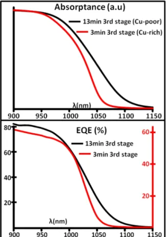
observe important differences in the IV parameters between the stoichiometric and the Cu-poor samples (Table 1). All the stoichiometric CIGS-based cells (obtained by KCN-etched Cu-rich films, i.e., with 3rd stage 8 min) exhibit very similarVOC(500 mV),JSC(28 mA cm2), and FF (fill factor) values (from 54 to 61%), resulting in similar efficiencies 8%. The use of Cu-poor CIGS (3rd stage >8 min) results in a strong improvement of the efficiency (h15 and 16% for 3rd stage¼9 and 13 min, respectively). The significantVOCenhancement ( þ150 mV) is the main cause of this efficiency gap. Temperature-dependent I–V measurements (IVT) were performed to better explain this feature. From these the activation energy of the main recombination path (Ea) can be extracted by linear extrapolation of the VOC values at high temperatures to 0 K. As Ea¼Eg for long 3rd stage cells, the main recombination path lies in the bulk. On the contrary, Ea is clearly lower thanEgfor short 3rd stage samples (Table 1 and Fig. SI1 in the Supporting Information, online at: www. pss-a.com). This indicates that the main recombination path for these samples is close to the CIGS-CdS interface, which explains the significant drop inVOC[8]. Two differences can be observed in the EQE spectra when stoichiometric CIGS is used instead of Cu-poor (Fig. 1a). Thefirst observation is related to the carrier collection, which decreases signifi -cantly in the long wavelength range of the absorber layer (700–1000 nm), indicating a shorter collection length. Table 1 VOC,Jsc, FF,Rsh,A,J0, andh, fromfittedI–Vmeasurements. Results represent average values from the 8 cells of each sample.
CGI (Cu/(InþGa)) ratio determined by energy dispersive spectroscopy (EDX).Egextracted from linear extrapolation of EQE.Eais the
VOCextrapolation at 0 K from IVT.
3rd stage length (min) 0 3 5 8 9 13
VOC(mV) 503 499 502 492 647 674 Jsc(mA cm2) 29.1 28.1 28.0 27.2 32.4 32.5 FF (%) 54 58 60 61 73 75 Rsh(Vcm2) 250 227 214 169 700 1373 A 3.1 2.7 2.6 2.1 1.9 1.6 J0(A cm2) 6105 3105 2105 4106 1107 1108 h(%) 8.0 8.1 8.4 8.1 15.2 16.5 CGI 1.7 1.4 1.3 1.0 0.92 0.87 Eg(eV) 1.18 1.17 1.17 1.14 1.14 1.14 Eg/qVOC(eV) 677 671 668 648 493 466 Ea(eV) 0.88 0.89 1.18
This observation appears to be in contradiction with the claimed superior transport properties of the stoichiometric CIGS. However, the collection length depends on both; the homo interfaces (grain boundaries) and the hetero interfaces
(with back contact and buffer layer) as well as on the transport properties of the absorber material itself. Thus, one can deduce that the decreased collection length is due to degraded interfaces, despite the reported better bulk CIGS transport properties [1, 2].
The second observation is related to the near-absorption edge region (1000–1100 nm): the transition is steeper for stoichiometric CIGS solar cells than for the Cu-poor ones, as already observed by several authors [25, 26]. According to the model by Klenk [27], EQE(l)¼IQE(l)K(l), with IQE(l)¼[1exp(a(l)Leff)], a is the absorption coeffi -cient of CIGS andK(l) represents the ratio of incident light that effectively reaches the absorber (withK(l)<1, due to absorption in the CdS and window layers, plus reflection losses). In this l range, we can consider that only a(l) significantly varies. Based on that, the steeper evolution of the EQE in the near bandgap region can be attributed to improved absorption properties, i.e., steeper absorption edge and less tails. This conclusion is supported by absorptance measurements on lifted-off samples from the same batch, where a similar evolution is observed (Fig. 2).
3.2 One-step gallium post-deposition treatment
In order to solve the VOC and JSC losses observed with stoichiometric CIGS, we developed a Ga-based surface
Figure 1 External quantum efficiency measurements. (a) Cu-poor sample in black (CGI¼0.92/0.87 for the dotted/full lines, respectively), Cu-rich in red (CGI¼1.4/1.0 for dotted/full line). (b) Cu-poor sample in black, samples from same Cu-rich batch in red: full/dashed/dotted¼not treated/treated with 494 K annealing (remains Cu-rich)/treated with 523 K annealing (turns Cu-poor). Full: not treated, dashed/dotted: temperature of annealing step for surface treatment¼494 K/523 K. One can observe that the sample remains Cu-rich with 494 K annealing, but turns Cu-poor with 523 K. Inset is zoom around the bandgap region. (c) Cu-poor sample in dashed black. Cu-rich samples from same batch with/ without low-high (LoHi) treatment in gray and red, respectively.
Figure 2 Comparison of EQE and absorption measurements for the same wavelength range.
In treatment successfully used on stoichiometric CIS to solve the same problems (see details in Section 2). To verify that only the CIGS surface is affected by the treatment and not the whole absorber is not as straight forward as it is in the CIS material. Here, the comparison of the steepness of the near bandgap edge EQE before and after Ga–Se treatment is used to attest that the CIGS layer stays mainly stoichiometric. Indeed, if either too much gallium is provided, the temperature is too high or the annealing time is too long, we clearly observe that the steepness decreases back to lower values as observed for Cu-poor CIGS (Fig. 1b). Our explanation is that with“soft”conditions, only the surface of the CIGS layer is modified, keeping the bulk stoichiometric with the associated steep absorption edge. But if we provide too much energy (and/or Ga), the entire CIGS layer turns Cu-poor, with the associated decreased steepness. Previous work supports that hypothesis: it was observed by Auger electron spectroscopy that only thefirst tens of nanometers can be modified by similar treatments (In–Se) on similar material (CuInSe2), provided moderate temperature is applied during such a treatment [12]. In addition to the parameters listed above, we observed that the magnitude of the Se-flux during the Ga surface treatment plays a major role on the impact of this treatment on the photovoltaic properties. Temperature value and profile during the treatment has been tuned to keep absorbers stoichiometric (values are found in the experimental section). The two remaining parameters are the fluxes of Se and Ga. To study and optimize them, two similar batches of stoichiometric CIGS (3rd stage¼6 min) have been prepared (four identical samples per batch). Results as measured byI–Vare shown in Table 2. For each batch, one sample is kept untreated, and Ga surface treatments of 20, 60, and 180 s. have been performed on the three other samples. For one batch (B), the Seflux during the Ga surface treatment was the same as that used during the growth of the absorber, leading to samples named HiSe-20, HiSe-60, and HiSe-180. For the other batch (A), the Seflux during the Ga surface treatment was lowered by a factor of 10. Resulting samples are named LoSe-20, LoSe-60, and LoSe-180. Similar IV/EQE parameters of the
between them are reasonable. Table 2 shows the evolution of the VOC andJSC with the amount of Ga treatment for each series, compared to a Cu-poor reference. This Cu-poor reference was grown on the same day with the same conditions (just slightly longer 3rd stage) to ensure the comparability especially the same GGI value and gradient. Thefirst observation is that theVOCvalues of the untreated stoichiometric samples are much lower than those obtained with the Cu-poor CIGS (425 vs. 675 mV). For a small amount of Ga (LoSe-20 and HiSe-20), theVOCincreases to 525 mV regardless the selenium flux. If the treatment is performed under high Se flux, the VOC increases again together with the Ga content (up to 590 mV for HiSe-Ga180). On the other side, with low-Seflux, theVOCdrops for higher Ga content, leading to very low current and voltage for the LoSe-Ga180 sample. We did not further investigate the deeper cause of this behavior. The second important difference is that theJSCslightly increases for the HiSe treatments, while it strongly increases and reaches values up to the level of the Cu-poor reference for the LoSe samples. Improvement of the EQE in the long wavelength regime on LoSe-treated samples indicates an increase in the collection length that results in this restoredJSC(not shown here but similar to “LoHi treatment,”Fig. 1c).
3.3 Two-step gallium post-deposition treatment
A treatment under low-Seflux appears to be mandatory to restore theJSC, but high Seflux is key to obtaining a higher
VOC. The increase in the VOC can be explained by an improved CIGS/CdS interface, due to the formation of a thin Cu-poor CIGS layer during the Ga–Se treatment (i.e., leading to the stack: stoichiometric-CIGS/Cu-poor CIGS/CdS). IVT measurements on similar samples (see Fig. SI2 in the Supporting Information) show an increase ofEa, supporting this explanation. The longer collection length (that results in aJSCincrease) can be partially explained by the improved CIGS/CdS interface. Our hypothesis is that in stoichiometric CIGS, the reduction of the collection length is mainly caused by problems at the homo-interfaces (grain boundaries). When the Ga–Se treatment is performed under HiSe flux, Table 2 Physical parameters determined in the same way as in Table 1. All samples from batches A and B are stoichiometric for both with and without surface treatment. Sample C is a Cu-poor reference.
batches A A A A B B B B C
treatment no LoSe20 LoSe60 LoSe180 no HiSe20 HiSe60 HiSe180 no
VOC(mV) 427 527 505 – 420 526 559 589 686 JSC(mA cm2) 30.5 32.7 32.7 – 29 30.7 29.8 29.9 33.6 FF (%) 56 57 62 – 57 61 67 57 76 Rs(Vcm 2 ) 0.4 0.4 0.6 – 0.5 0.3 0.6 0.3 0.2 Rsh(Vcm2) 288 251 204 – 336 280 246 260 791 A 2.7 1.8 2.1 – 2.6 2.6 1.7 3.5 1.9 J0(A cm2) 7105 4107 5106 – 6105 1105 1107 8105 3108 h(%) 7.3 11.6 10.3 – 7 9.9 11.3 10.2 17.4 Eg(eV) 1.16 1.16 1.16 1.16 1.16 1.16 1.16 1.16 1.15 Eg/qVOC(eV) 733 633 655 – 740 634 601 571 464
mostly the surface is changed and the grain boundaries are still reducing the collection length. But under LoSeflux, the reactivity of the species are different, leading to passivation of the grain boundaries, which ultimately improves the collection length, but with a smaller improvement of the CIGS/CdS interface.
Considering these hypotheses, a new Ga–Se treatment has been designed in order to take advantage of both favorable features. This treatment is named the “LoHi treatment” and is the succession of both the LoSe-Ga60 and the HiSe-Ga60. Starting with LoSe-Ga60, which is expected to passivate the grain boundaries resulting in a good collection length and ultimately JSC. Followed by HiSe-Ga60 to form a good CIGS/CdS interface in order to enhance theVOC.
AsJSC values as high as those of Cu-poor have been achieved by Ga–Se treatments under low Se, the major remaining challenge for stoichiometric CIGS is to reach a VOCas high as that obtained from Cu-poor. A common way to discuss the interface quality regardless of the CIGS Eg/GGI is to consider the VOC deficit (EgVOC) as it is expected to be constant in theEgrange of this study. Several
Cu-poor (17)/not treated stoichiometric (18)/LoHi treated stoichiometric (11) CIGS samples have been prepared in order to compare theVOC-deficit versusEg/GGI evolution. The bandgaps of all the samples are in the range of 1.09–1.21 eV. For each type, when different samples have the same bandgap value (rounded to the hundredth of eV), only the lowerVOC-deficit (of all the cells of a sample) is considered (that filtering rules-out VOC-deficit due to additional problems). Results are presented in Fig. 3. For each type of sample, the VOC deficit is not significantly varying with the bandgap, ruling out a problem of band alignment. Average values for VOC-deficit of Cu-poor/ untreated stoichiometric/LoHi treated stoichiometric are 456, 667, and 540 mV, respectively. By the LoHi treatment the relativeVOC-deficit compared to Cu-poor was reduced by a factor of2.5 (from210 to85 mV). Improvement of the CIGS/CdS interface explains this increase of the VOC, as confirmed by IVT measurements (two samples from the same batch,Eg¼1.11 eV;Ea¼0.77 and 1.11 eV for untreated and LoHi treated samples, respectively, see Fig. SI3 in the Supporting Information).
Finally (Table 3), the most efficient LoHi treated sample is 14.4% (average of six cells, with champion cell¼15.4%, area including grids¼0.4 cm2) obtained for a bandgap of 1.15 eV. Our best Cu-poor with the same bandgap (still average of six cells) has an efficiency of 17.6%, with higherVOC(682 vs. 587 mV), FF (76 vs. 68 %) but lower
JSC(34.0 vs. 35.9 mA cm 2
, i.e.,þ5.6%). TheJSCobtained from integrated EQE (active area, AM 1.5 spectrum) confirms this noticeable improvement (32.9 vs. 35.0 mA cm2, i.e., þ6.4%) (Fig. 1c). The steep EQE transition around the bandgap attests that the absorber is still mostly stoichiometric after the LoHi treatment. The main reason of this improved JSC is a higher EQE for the long wavelength region (800–1000 nm). Please note that as space charge region is shorter for stoichiometric compared to Cu-poor CIGS, identical transport properties should results in shorter collection length, i.e., lower EQE at long wavelength. Thus, and considering the observations presented in Fig. 2, the small but visible improvement of EQE in that region strongly supports superior transport properties for LoHi treated stoichiometric sample compared Figure 3 VOCdeficit (Eg/qVOC) in mV versusEg(in eV) for
untreated poor (in black), untreated rich (in gray), and Cu-rich treated (in red) samples.VOCis the average of eight cells in a
sample. Dashed lines are averageVOCdeficit for each sample type.
Table 3 Physical parameters determined in the same way as in Table 2. AsI–Vmeasurements were performed with a cold halogen lamp, irradiancefluctuations have to be considered, making it more relevant to discuss the average instead of the max values ofJSC/efficiency.
sample untreat LoHi average LoHi champion Cu-poor average Cu-poor champion
VOC(mV) 438 587 589 682 678 JSC(mA cm2) 30.8 35.9 37.8 34 34.7 FF (%) 55 68 69 76 76 Rs(Vcm2) 0.4 0.5 0.5 0.2 0.3 Rsh(Vcm2) 167 378 330 791 811 A 2.7 2 1.9 1.9 1.8 J0(A/cm 2 ) 7105 4107 2107 3108 1108 h(%) 7.5 14.4 15.4 17.5 17.8 Eg(eV) 1.15 1.15 1.15 1.15 1.15
transport properties of the stoichiometric versus Cu-poor CIGS, that is counterbalanced by degraded grain boundaries without optimized Ga–Se treatment. The improvement of JSC in comparison with Cu-poor samples of the same bandgap requires a good correlation between the amount of Ga provided during the surface treatment and the GGI ratio of the untreated CIGS. Fine-tuning of this parameter may provide room for further improvement. Moreover, one can expect higher efficiencies using CIGS absorber with higher GGI/Eg, as the 85 mV loss versus Cu-poor will be relatively less important. Moreover, the champion cell exhibits aVOC deficit and FF of 551 mV and 69%, respectively, but values of 523 mV and 71% have been observed for other treated stoichiometric samples.
4 Conclusions In summary, stoichiometric CIGS
cells have been compared to Cu-poor ones. A strong reduction in the VOCis observed, and explained by a bad stoichiometric-CIGS/CdS interface. At the same time, JSC reduction is attributed to deteriorated grain boundaries, limiting the collection length. A Ga–Se treatment has been developed to reduce these problems. When such a treatment is performed, the surface of the CIGS absorber turns Cu-poor, resulting in a CIGS-stoichiometric/CIGS Cu-poor/CdS stack with better absorber/buffer interface that reduces the VOCdeficit. BestVOC-deficit values are obtained under high-Seflux, but still lower than those of the Cu-poor references (difference is found to be 85 mV regardless of the GGI ratio). Moreover, performing all or part of the treatment under low Se flux passivates the grain boundaries. Successive treat-ments under low and high Se fluxes result in a champion treated stoichiometric CIGS cell of 14.4% efficiency, with
6% current increase versus Cu-poor reference due to the longer collection length of carriers attributed to the better transport properties of stoichiometric absorbers.
Supporting Information Additional supporting infor-mation may be found in the online version of this article at the publisher’s web-site.
Acknowledgements This work was supported by the Fonds national de la Recherche Luxembourg in the framework of the CURI & CURI-K CORE-projects. Authors would like to thank Ashley Finger for absorptance measurements, Thomas Schuler and Michele Melchiore for technical support.
References
[1] S. Nomura, J. Itoh, and T. Takizawa, Jpn. J. Appl. Phys.32, 97 (1993).
[2] S. Siebentritt, A. Gerhard, S. Brehme, and M. C. Lux-Steiner, in: Proc. MRS (2011), p. 668.
119
[4] L. G€utay, D. Regesch, J. K. Larsen, Y. Aida, V. Depredurand, and S. Siebentritt, Appl. Phys. Lett.99, 151912 (2011). [5] P. Jackson, D. Hariskos, R. Wuerz, O. Kiowski, A. Bauer,
T. M. Friedlmeier, and M. Powalla, Phys. Status Solidi RRL
9, 28 (2015).
[6] E. Wallin, U. Malm, T. Jarmar, O. L. Edoff Marika, and L. Stolt, Prog. Photovolt.: Res. Appl.20, 851 (2012). [7] R. Scheer and H.-W. Schock, Chalcogenide Photovoltaics:
Physics, Technologies, and Thin Film Devices (Wiley-VCH, Weinheim, 2011).
[8] M. Turcu, O. Pakma, and U. Rau, Appl. Phys. Lett.80, 2598 (2002).
[9] H. Wilhelm, H.-W. Schock, and R. Scheer, J. Appl. Phys.
109, 084514 (2011).
[10] V. Depredurand, D. Tanaka, Y. Aida, M. Carlberg, N. Fevre, and S. Siebentritt, J. Appl. Phys.115, 44503 (2014). [11] T. Bertram, V. Depredurand, and S. Siebentritt, in: 40th IEEE
Photovolt. Spec. Conf. PVSC, pp. 3633–3636 (2014). [12] Y. Aida, V. Depredurand, J. K. Larsen, H. Arai, D. Tanaka,
M. Kurihara, and S. Siebentritt, Prog. Photovolt.: Res. Appl.
23, 754 (2015).
[13] A. M. Gabor, J. R. Tuttle, D. S. Albin, M. A. Contreras, R. Noufi, and A. M. Hermann, Appl. Phys. Lett. 65, 198 (1994).
[14] J. Kessler, C. Chityuttakan, J. Lu, J. Sch€oldstr€om, and L. Stolt, Prog. Photovolt.: Res. Appl.11, 319 (2003). [15] T. Godecke, T. Haalboom, and F. Ernst, Z. Metallkd.91, 622
(2000).
[16] J. C. Mikkelsen, J. Electron. Mater.10, 541 (1981). [17] S. Niki, P. J. Fons, A. Yamada, Y. Lacroix, H. Shibata,
H. Oyanagi, M. Nishitani, T. Negami, and T. Wada, Appl. Phys. Lett.74, 1630 (1999).
[18] T. P. Hsieh, C. C. Chuang, C. S. Wu, J. C. Chang, J. W. Guo, and W. C. Chen, Solid-State Electron.56, 175 (2011). [19] Y. Hashimoto, N. Kohara, T. Negami, M. Nishitani, and
T. Wada, Jpn. J. Appl. Phys.35, 4760–4764 (1996). [20] M. I. Alonso, K. Wakita, J. Pascual, M. Garriga, and
N. Yamamoto, Phys. Rev. B63, 075203–075215 (2001). [21] P. D. Paulson, R. W. Birkmire, and W. N. Shafarman, J. Appl.
Phys.94, 879–888 (2003).
[22] P. Jackson, D. Hariskos, R. Wuerz, W. Wischmann, and M. Powalla, Phys. Status Solidi RRL8, 219 (2014). [23] S. Siebentritt, G. Rey, A. Finger, D. Regesch, J. Sendler, T. P.
Weiss, and T. Bertram, Sol. Energy Mater. Sol. Cells, in press, http://dx.doi.org/10.1016/j.solmat.2015.10.017. [24] A. R. Burgers, J. A. Eikelboom, A. Schonecker, and W. C.
Sinke, in: Conf. Rec. 25th IEEE Photovolt. Spec. Conf. 1996, pp. 569–572 (1996).
[25] J. R. Tuttle, D. Albin, R. J. Matson, and R. Noufi, J. Appl. Phys.66, 4408 (1989).
[26] S. Chichibu, T. Mizutani, K. Murakami, T. Shioda, T. Kurafuji, H. Nakanishi, S. Niki, P. J. Fons, and A. Yamada, J. Appl. Phys.83, 3678 (1998).
[27] R. Klenk and H.-W. Schock, in: Proc. 12th Eur. Photovolt. Sol. Energy Conf. (1994).