EFFECTS OF SUBSTRATE TEMPERATURE OF WINDOW LAYER ON THE PERFORMANCE OF SnxSey/ZnO:Al P-N JUNCTION SOLAR CELL
JOHN GITONGA MBAE (B.EdSc) I56/CE/25987/2011
A thesis submitted in partial fulfillment of the requirements for the award of the Degree of Master of Science (Electronics and Instrumentation) in the School of Pure and Applied Sciences of Kenyatta University
DECLARATION
This thesis is my original work and has not been presented for the award of a degree or any other award in any other University
Mbae John Gitonga
Signature………Date.……… Department of Physics
Kenyatta University
This thesis has been submitted for examination with our approval as University Supervisors
Dr. Mathew M. Munji
Signature………Date.……… Department of Physics
Kenyatta University
Dr. Robinson J. Musembi
Signature………Date.……… Department of Physics
DEDICATION
ACKNOWLEDGEMENTS
I would like to sincerely thank my university supervisors; Dr. Mathew M. Munji (Kenyatta University) and Dr. Robinson J. Musembi(University of Nairobi) for their unwavering guidance throughout the research period.May the almighty God give you great wisdom, long life and bless the work of your hands.
I acknowledge the Vice Chancellor of Kenyatta University Prof. Olive Mugenda for availing an encouraging research environment especially free internet connection for online research. My other heart felt gratitude’s goes to the entire staff members of the Department of Physics, Kenyatta University under the leadership of Dr. Omar Hashim for being supportive throughout the research period. I also acknowledge the technical staff of Physics laboratory led by Mr. Frindrick Mudimba for their technical support and availing apparatus while carrying out my laboratory work. More so, Mr. AntonyNjagi a technician fromDepartment of Chemistry (Kenyatta University) for his assistance during the preparation of ingotsand generally doing things that were beyond the call of his duty. Not to forget is Mr.MuthokaBoniface of University of Nairobi who is a senior technician in the solid state physics laboratory who assisted and trained me on how to make optical and electrical measurements of the solar cell.
TABLE OF CONTENTS
DECLARATION... ii
DEDICATION ... iii
ACKNOWLEDGEMENTS ...iv
TABLE OF CONTENTS ... v
LIST OF TABLES ... x
LIST OF FIGURES ...xi
ABBREVIATIONS AND ACRONYMS ... xiii
ABSTRACT ... xvi
CHAPTER 1 ... 1
INTRODUCTION ... 1
1.1 Background to the study ... 1
1.2 Statement of the problem ... 2
1.3 Objectives ... 3
1.3.1 General objective ... 3
1.3.2 Specific objectives ... 3
1.4 Rationale of study... 3
CHAPTER 2 ... 5
2.1 Introduction ... 5
2.2 Thin film materials for solar cell ... 5
2.3 Classification of solar cells ... 6
2.4 Related work done ... 6
2.5 Zinc Oxide based solar cells ... 9
CHAPTER 3 ... 10
THEORETICAL CONSIDERATIONS ... 10
3.1 Introduction ... 10
3.2 Theory of thin film solar cell ... 10
3.3 Optical characterization of thin films ... 12
3.3.1 Optical behavior of thin films ... 12
3.3.2 Optical properties of crystalline and amorphous materials ... 14
3.3.3 Band gap energy ... 15
3.3.4 Optical reflectance ... 15
3.3.5 Optical transmission ... 16
3.3.6 Absorption coefficient ... 16
3.3.7 Direct and indirect band gap ... 17
3.3.8 Refractive index... 19
3.4 Electrical Characterization of thin films ... 20
3.6 P-N junction parameters ... 23
3.6.1 Short Circuit Current (ISC) ... 23
3.6.2 Open Circuit Voltage (Voc) ... 24
3.6.3 Fill Factor (FF) ... 24
3.6.4 Efficiency (η) ... 25
3.7 Thin film deposition Techniques ... 25
3.8 Physical models ... 26
3.8.1 The O’ Leary-Johnson-Lim (OJL) model ... 26
3.8.2 The Drude model ... 28
3.8.3 Harmonic Oscillator... 28
3.9 Structural and elemental characterization ... 29
3.9.1 X-ray fluorescence (XRF) ... 29
CHAPTER 4 ... 31
MATERIALS AND METHODS ... 31
4.1 Preparation of ingots... 31
4.1.1 Tin Selenide (SnxSey)... 31
4.1.2 Aluminium doped Zinc Oxide (ZnO:Al) ... 32
4.2 Evaporation and deposition SnxSey thin films ... 33
4.3 Evaporation and deposition of ZnO:Al thin films ... 35
4.5 Optical measurements ... 37
4.6 Sheet resistivity measurements ... 38
4.7 Rapid Thermal Processing ... 40
CHAPTER 5 ... 42
RESULTS AND DISCUSSION ... 42
5.1 Optical characteristics of ZnO:Al ... 42
5.1.1 Optical spectra of ZnO:Al thin films ... 42
5.1.2 Thickness of thin films ... 46
5.1.3 Simulated and experimental Graph ... 47
5.1.4 Optical bandgap energies ... 47
5.2 Optical characteristics of SnSe ... 49
5.2.1 Transmittance data against wavelength ... 49
5.2.2 Transmittance, Reflectance and Absorbance averages in the visible region ... 50
5.2.3 Simulated and experimental Graph ... 51
5.2.4 Optical bandgap energies ... 51
5.2.5 Refractive index... 53
5.2.6 Absorption coefficient for tin selenide ... 54
5.3 Optimized deposition parameters of ZnO:Al and SnxSey thin films ... 55
5.4 Electrical characterizationofZnO:Al and SnSethin films ... 55
5.4.2 SnSethinfilm ... 57
5.5 Elemental composition for SnxSey and ZnO:Al thin films ... 58
5.5.1 Elemental composition for SnxSey thin films ... 58
5.6 Solar cell fabrication... 60
CHAPTER 6 ... 64
CONCLUSIONS AND RECOMMENDATIONS ... 64
6.1 Conclusions ... 64
6.2 Recommendations ... 65
LIST OF TABLES
Table 4.1: The periodic table ... 31
Table 4.2: Tin selenide samples showing various tin to selenium ratios. ... 32
Table 4.3: Zinc oxide sample showing various aluminium doping percentage... 32
Table 4.4: Zinc oxide samples with 5% aluminium deposition temperature. ... 36
Table 5.1: Average transmittance of ZnO:Al within different spectrum regions ... 43
Table 5.2:ZnO doped with aluminiumand calculated bandgap energyvalues ... 48
Table 5.3: Band gap energy values and ratios of Se/Sn by mass ... 52
Table 5.4:Optimized deposition parameters forZnO:Al and SnxSeythin films ... 55
LIST OF FIGURES
Figure 3.1: Diagram of p-n heterojunction solar cell ... 11
Figure 3.2: Schematic diagram for optical transmission measurement. ... 12
Figure 3.3: Direct and indirect band gap ... 18
Figure 3.4: A schematic diagram showing the arrangement used to measure sheet resistivity ... 20
Figure 3.5: Schematic diagram for measurement of diode characteristics ... 22
Figure 3.6: Band diagram of p-n junction solar cell showing generation of electron-hole pair due to photon absorption. ... 23
Figure 3.7: Parabolic bands with tail states exponentially decaying into the band gap ... 27
Figure 4.1:Edwards Auto 306 coating unit ... 34
Figure 4.2: Schematic diagram of deposition by evaporation . ... 35
Figure 4.3: The UV-VIS-NIR Spectrophotometer 3700 DUV (Shimadzu) ... 38
Figure 4.4:Keithley 2400 source meter for measurement of sheet resistance ... 39
Figure 4.5: Schematic diagram of a four point probe used to measure surface sheet resistivity 39 Figure 4.6:Nabertherm programmable furnace model LH 15/14 ... 40
Figure 4.7: Schematic diagram for Nabertherm programmable Furnace, model LH 15/14 ... 41
Figure5.1:Graph oftransmittancespectra of ZnO:Al films ... 42
Figure 5.2: Graph of average transmittance in ZnO:Al within the visible region ... 44
Figure5.3:Graph ofreflectancespectra of ZnO:Al films due to doping ... 44
Figure5.4:Graph ofreflectancespectra of ZnO:Al films due to deposition temperature ... 45
Figure5.5:Graph offilm thickness with deposition temperature ... 46
Figure5.6: Simulatedand experimental graphfor 5 % aluminium doped ZnO ... 47
Figure5.7: Graph of band gap energy with doping concentration ... 48
Figure 5.9: Graph of transmittance, absorbance and reflectance in visible region. ... 50
Figure5.10: Simulatedand experimental graphfor Tin selenide at a ratio of 1:1 ... 51
Figure 5.11: Graph of variation of optical band gap energy with different Sn:Se ratios ... 53
Figure 5.12: Graph of refractive index (n) as a function of wavelength ... 53
Figure 5.13: The absorption coefficient against wavelength for tin selenide... 54
Figure 5.14: Graph of resistivity and conductivity as a function of deposition temperature ... 56
Figure 5.15: Graph of resistivity and conductivity as a function of tin–selenium ratio ... 57
Figure 5.16:PhotographofMiniPal2 XRFSpectrometer ... 58
Figure 5.17: XRF spectrum for optimized ZnO:Al deposited at 510 K ... 59
Figure 5.18: XRF spectrum for optimized SnSe (ratio 1:1). ... 59
Figure5.19:Schematicdiagram of fabricatedZnO:Al/SnSe/AlP-N heterojunctionsolar cell ... 61
Figure 5.20:Solar simulator ... 61
LIST OF ABBREVIATIONS AND ACRONYMS
Al - Aluminium
Ar - Argon
AZO - Aluminium doped Zinc oxide
CBD - Chemical Bath Deposition
CVD - Chemical vapour deposition DC - Direct current
DUV - Deep Ultra Violet E - Input light irradiance Ec - Conduction band Ef - Fermi level
Eg - Band gap energy
eV - Electron Volt
Ev - Valenceband Energy
FF - Fill factor
HEP - Hydroelectric power
Io - Dark saturated current
IR - Infra Red
Isc - Short circuit current
LED - Light emittingdiode.
MBE - Molecularbeam epitaxy
MOCVD - Metal oxide chemical vapour deposition mV - millivolts
PECVD - Plasma Enhanced Chemical Vapour Deposition PL - Photoluminescence
Pm - Maximum Power
PV - Photovoltaic
PVD - Physical vapour deposition
Se - Selenium
SEM - Scanning electron microscopy
Sn - Tin
SnxSey - Tin selenide
TEM - Transmission Electron Microscope
TCO - Transparent Conducting Oxide
UV - UltraViolet
VIS-NIR - Visible to near infrared
Voc - Open Circuit Voltage
XRF - X-Ray flourecence
Zn - Zinc
ZnO:Al - Aluminum doped Zinc Oxide
Ωcm - ohm Centimeter
ABSTRACT
CHAPTER 1 INTRODUCTION
1.1 Background to the study
The demand for energy has increased steadily with the growing population and embracing of new technologies. More households and institutions will require connection to already overstretched national grid power supply. Currently, over 90% of power in the Kenyan national grid is from hydroelectric power (HEP)(Oludhe, 2011). Climatic change due to destruction of natural vegetation cover and global warming among others has led to water levels in HEP dams reducing. This has occasioned the frequent power rationing and in some cases total black outs which interrupt livelihood of citizen and economic growth.
devices. Photovoltaic is therefore a process of obtaining electricity directly from the abundant solar energy. A solar cell acts as a transducer within the device converting the solar energy into electricity for powering internal circuit or for storage purpose. The process of photovoltaic power generation is reliable as compared to hydroelectric generation whichis severely affected by low level of dam water. Its production does not involve moving parts thus making its operation and maintenance costs relatively low. Solar energy is also easy to install (Fardo andPatrick, 1985).
Installing electricity from HEP in remote areas has become expensive due to poor infrastructure. Installation costis also high as it requires highly skilled manpower. Harnessing of solar energy will help reduce air pollution and preserve ecological system on the earth. The major advantage of photovoltaic system is that they tap an almost inexhaustible resource that is free of charge and available everywhere in the world. This research work aims at establishing the optimum deposition parameters of thin films in the fabrication of SnxSey-ZnO:Al solar cell.
1.2 Statement of the problem
Conventionalenergy sourcessuchasfossilfueland crudeoilimpact negatively ontheenvironmentmainly duetopollution. One of the solutions to this perennial problem is use of solar energy. Variouselements and compounds have beenstudiedto fabricate thinfilm semiconductorsforthesolar cellapplications. Apart from the materials used in the cell fabrication, the performance of solar cell also depends on the technique used and deposition parameters.Althoughsiliconbased
technologyhasbeenextensivelyusedinsolarcells,itisveryexpensive.Hencethereisneed
contribution of optimized deposition temperature and doping percentage to the performance of the solar cell is studied.
1.3 Objectives
1.3.1 General objective
To determine the effect of varied deposition temperature of window layer and characterize SnxSey-ZnO:Althin films for solar cell applications.
1.3.2 Specific objectives
i) To determine the optimum doping concentration in ZnO:Aland optimum ratio in SnxSey thin films.
ii) To investigate the effect of deposition temperature on the optical and electrical properties of ZnO:Al thin films.
iii) To electrically characterize SnxSey thin film using four point probe method.
iv) To fabricate and characterize SnxSey-ZnO:Al p-n junction solar cell at optimum doping concentrations and deposition temperature using solar cell simulator.
1.4 Rationale of study
CHAPTER 2 LITERATURE REVIEW
2.1 Introduction
A solar cell is a device that is highly embraced both in rural and urban areas to provide an alternative source of electrical power to the ever increasing demand.Thetechnologies applied in the manufacture of solar cells is wide with thin film technology being commonly applied as it ensures charges generated have short diffusion length, quantity of material used is relatively small and the cell has high charge recombination rate (Fuller et al.,1954). The photoelectric properties of thin films are determined by their chemical composition, the content and type of impurities in the thin film or on its surface, crystal structure of the thin film and the types and density of structural defects (Ogwu et al., 2007). This chapter gives a background on the recent developments and highlights the ongoing research areas in solar cell technology. Special attention is focused on how to improve the efficiency of a solar cell by optimizing the material composition and deposition parameters.
2.2 Thin film materials for solar cell
aimed at improving the efficiency of solar cells, developing better fabrication technologies and coming up with new and better solar cell materials.
2.3 Classification of solar cells
Solar cells are classified into three generations which indicates the order of emergence. The first generation solar cells consist of large area, high quality and single junction devices. They involve high energy and labour inputs which prevent any significant progress in reducing production costs. The second generation materials were developed to address energy requirement and solar cells production cost(Hirshman et al., 2008). Techniques such as solution deposition, vapour deposition, electroplating and use of Ultrasonic Nozzles have advantages since they reduce high temperature processing. Successful second generation materials include cadmium telluride (CdTe), copper indiumgallium selenide, amorphous and micromophous silicon (Hirshman et al., 2008). Third generationtechnology enhances the poor electrical performance of second generation technology and maintains low production costs. Modernresearches target high conversion efficiency of 30-60% while retaining low costs; and one attempt to achieve higher efficiencies is the use of thermal generation by UV light to enhance voltage collection, and concentration of incident spectrum (Green, 2002). The main strategies used to reduce the cost of photovoltaic electricity are increasing the efficiency and decreasing the cost of solar cells per generated unit of power.
2.4 Related work done
opticalbandgap of the tin selenideliedbetween1.18-1.75±0.05eVmaking it a suitable absorber layer in a solar cell. A sample of Sn:Sewith a ratioof1:1registered thelowestbandgapenergyand was used in the final fabrication of the cell.Thin filmthicknessrangedbetween49.5-69.5±0.5nmasobtained from thescout 98 software.The resistivity of tin selenide also decreased as the ratio of tin to selenium approached 1:1 reaching the lowest value of 23.4Ωcm at 4%doping level. The fabricated SnxSey/ZnO:Al p-n junction solar cell was characterized using a solar simulator and from the I-V characteristics obtained, the short-circuit current Isc was 1.06mA, the open circuit voltage was observed to be Vocwas0.59V, and overall conversion efficiency of 0.41%.
ZnO:Al thin films grown in Argon (Ar) shows a weak increase in both carrier concentration and mobilization when deposited at various deposition temperature(O’Donnell and Chen,1991). ZnO:Al was deposited on surface of SnO2:F substrate. The degradation extent was monitored and its function as a back reflector studied. Samples that had been coated with ZnO:Al had little degradation and had very good solar cell properties (Zhao et al., 2002). The resistivity of ZnO:Al films was affected by the percentage of Al2O3. The resistivity changed due to variation in deposition temperature which affected the thickness of the film. The optical, electrical and structural properties heavily depended on deposition parameters (Tang et al., 2000).
prepared by evaporation method. The spectral was scattered within a range of wavelengths, 150-300nm. They reported electrical resistivity of between 3.0-8.1Ωcm. Sharma et al. (2005) prepared and characterized nanocrystalline SeSn (n-SnSe) thin film by thermal evaporation of the material in the presence of argon carrier gas. The band gap value increased to (2.18±0.01) eV as compared to the bulk value of (1.68±0.01) eV.
lied between 1.37eV to 1.73eV. This made it a good absorber layer hence realizing improved cell efficiency.
2.5 Zinc Oxide based solar cells
Ahmed et al. (2006) synthesized Al doped SnO2 thin films with different percentages of Al on a glass substrate.He noted that the optical transmittance spectra of the films showed high transparency (~80 %) in the visible region and it increased with increase in Al doping in the films. The direct band gap of the films was measured for different concentration of Al and was found to be within the range of 3.87-4.21 eV. They observed that the Seebeck coefficient changes its sign at 12.05% of Al in the films indicating that below 12.05% of Al doping, SnO2: Al behaved as an n-type material and above this percentage it was a p-type material.
CHAPTER 3
THEORETICAL CONSIDERATIONS
3.1 Introduction
This chapter outlines the theory of deposition techniques and more specifically on thermal evaporation as the techniques adopted in this study. Also presented are theoretical backgrounds on solar cells, thin film resistivity measurements,optical characterization and structural properties of thin films.
3.2 Theory of thin film solar cell
Photovoltaic energy conversion in solar cells takes place through three essential steps (Markvart, 1998)namely:
(i) Charge generation: occurring in the absorber layer where photon absorption occurs to create electron hole pairs.
(ii) Charge separation: electrons crossing the potential barrier leaving hole behind.
(iii) Charge transport. Electrons flowing through the external circuit and recombining at the base.
The energy of incoming photons determines whether there will be charge generation or not. Photons with energy exceeding bandgap of the semiconductor under illumination are absorbed by electrons within the valence band. These electrons are excited to higher states and cross to the n-side of the semiconductor leaving behind a positive site called a hole(Markvart, 1998). These electrons flow through the external circuit and recombine later to create an electron – hole (E-H) pair at the junction. The existence of E-H pair at the junction generates a photocurrent which flows from the n-type to p-type. Once electrons crosses over, they are separated by some inbuilt electric field as shown in figures 3.1
Figure 3.1: Diagram of p-n heterojunction solar cell (Markvart, 1998). Depletion layer
p
h
ν
h
ν
n
3.3Optical characterization of thin films
3.3.1 Optical behavior of thin films
When incident photons strike a thin film, they interact with electrons of the films in a number of ways.A photon can be transmitted, reflected, scattered, absorbedor undergo luminescence. From these optical effects, we obtain optical constants. From a graph of photon energy as a function of absorption spectrum, a number of optical properties such as band gaps can be studied (Meieretal
2004). Photons with higher energy are absorbed by the electrons within the filled valence band and cross over to occupy the empty conduction band states. The absorption of radiations is due to electron transitions, formation of excitons and impurity states which form at the lowest forbidden energy gap(Rnjdar and Ali, 2007). The transitions of free carriers within energy bands produce an absorption continuum which increases with decreasing photon energy. The crystalline lattices absorb radiation, with the energy being given off as optical and acoustic phonons. Finally, at low energies, electronic transitions are observed between impurities and bands associated to them. These processes have important optoelectronics applications (Davis and Mott, 1970).
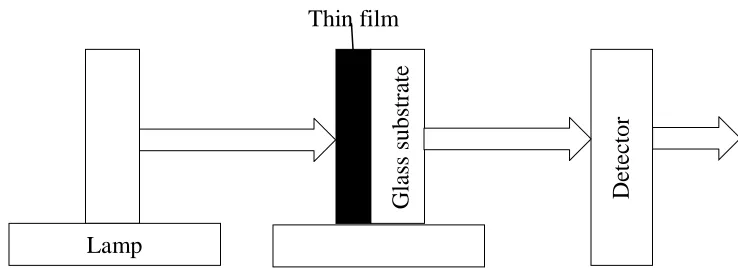
Figure 3.2: Schematic diagram for optical transmission measurement.
De
tec
tor
Lamp
Gla
ss
s
ubs
tr
ate
Figure 3.2 shows how values of transmittance and reflectance are obtained. The wavelength of the incident photons was adjusted to the required value by Spectrophotometer. The beam of intensity Iowas directed at the thin film of thickness (t) and relative transmission observed. The detector was used to measure the transmittance and reflectance. Photons with energies less than Egwere transmitted while those with energies greater than band gap (Eg) were absorbed. This gave accurate measurement of energy band gap,Eg. The amount of absorption depends on the thickness of the target thin film, wavelength of the incident photons and properties of the thin film. The intensity of photon transmitted It through the film of thickness.t is given by(Markvart, 1998):
𝐼𝑡 = 𝐼𝑜e−∝t 3.1
where Io is intensity of the incident photon, α is absorption coefficient. Rearranging equation3.1 we get expression for α as follows;
∝=1𝑡𝐿𝑛𝐼𝑜
𝐼𝑡(𝑐𝑚
−1) 3.2
The type of band gap (either direct or indirect) can be identified using absorption co-efficient values from the equation(Markvart, 1998):
ℎ𝑣𝛼 = 𝐴(ℎ𝑣 − 𝐸𝑔)12 3.3
where: 𝐸𝑔 is the material energy band gap, A is the energy dependent constant, h is the planks constant ,v is the frequency and𝛼 theabsorption coefficient. The value of 𝛼−1, give the average distance travelled by a photon before it gets absorbed. Transmittance of thin film was calculated from;
Transmittance (𝑇) = 𝐼𝑡
A beam of monochromatic light of sufficient energy, known frequency and intensity was shone onto the thin film. The detector was used to measure the intensity of the reflected light. The following equation gave the numerical value of reflectance;
Reflectance (𝑅) = 𝐼𝑅
𝐼𝑜 3.5
where IR and Io are intensity of the reflected and incident beams respectively.
3.3.2 Optical properties of crystalline and amorphous materials
The result of experiments carried out by Davis and Mott (1970) summarizes the behavior of amorphous semiconductors. The theory gives two important phenomena namely:
(i) Band structure of the materials,
(ii) The defect states or the tail of crystalline structure falls in the forbidden gap.
α(ω) = A(ђω-Eopt)2/ђω 3.6
Where Eopt is the optical energy gap, A Einstein coefficient,ђ reduced plank constant andω is the angular frequency.
When thescatter of (αђω) 1/2 versus (ђω) is extrapolated at the value of 𝛼 = 0,the optical energy gap is read directly on the x axis. This theory relates optical absorption has having relationship with forbidden indirect transition.
3.3.3 Band gap energy
This refers to the minimum energy possessed by a photon required to excite an electron in a semiconductor from its bound state to a free states so as to participate in conduction. The diagrammatic representation of a semiconductor has energy of electrons on the y axis and such diagrams are referred to as band diagram. The valence band denoted Ev is the lower energy level in a semiconductor, while conduction band Ec is the state at which an electron can be considered to be free. The energy difference between the conduction band and the valence band is called the band gap Eg(Markvart, 1998). Therefore bandgap is the lowest energy needed to excite an electron from valence band to conduction band. Excited electrons move to the conduction band and are free hence they participate in conduction within the semiconductor.This movement of electrons to the conduction band leaves an empty space which is considered to be positively charged and referred to as a hole. They form sites of charge recombination as electrons from the external circuit and surrounding atoms moves in these empty spaces.
3.3.4 Optical reflectance
amount of light incident(Markvart, 1998). A spectrophotometer is used to compare these intensities where a selected photon is directed on to the surface of thin film. The two intensities are compared by the reference called reflectance (R) which is usually expressed as percentageand is given as(Markvart, 1998),
Reflectance (R) = 𝐼𝐼𝑟
𝑜× 100 3.7
whereIoand Ir are intensities of the incident beams and reflected respectively.
3.3.5 Optical transmission
The bandgap of a material determines the amount of beam intensity that is transmitted through it. A low bandgap material will allow little photons to pass through since most of incident photons will be absorbed(Markvart, 1998). When photons with energies greater than band gap strike a thin film, they cause excitation. Electrons from the valence band gain sufficient energy and moves to the higher states. Intensities with lower energy than bandgap are transmitted through and they do not cause any excitation. The measure of transmittance therefore compares the incident intensity (Io) and the transmitted intensity (It) and is given by equation (3.8) shown(Markvart, 1998).
Transmittance (T) = 100
Io It
3.8
3.3.6 Absorption coefficient
range of incident light wavelength that is absorbed and also on nature of the material(Markvart, 1998). Light with energy that is below bandgap does not excite any electron to move from valence band to conduction band. This energy is not absorbed and is either transmitted through or lost as heat within the semiconductor materials. Due to this phenomenon, semiconductor materials are said to have a sharp edge in their absorption coefficient. The value of absorption coefficient for various semiconductor materials depends on wavelength of incident photons. The probability of absorbing a photon depends on the likelihood of having a photon and an electron interact in such a way as to move from one energy band to another(Markvart, 1998). For photons which have energy very close to that of the band gap, the absorption is relatively low since only those electrons directly at the valence band edge can interact with the photon to cause absorption. As the photon energy increases, not just the electrons have already energy close to that of band gap can interact with the photon resulting in absorption of photon but there is extra energy lost as heat and lattice vibrations.
There is a relationship between the extinction coefficient k,and the absorption coefficient,α, and is given by the(Markvart, 1998);
𝛼 =
4πkλ 3.9
3.3.7 Direct and indirect band gap
conduction band and top of a valence band occurs at the same value of electron momentum, then the material is said to have a direct band gap(Markvart and Castener, 2005).
In an indirect band gap semiconductor, the minimum in the conduction band energy occurs at a different value of momentum to the maximum energy of the valence band.
Figure 3.3:Direct and indirect band gap(Markvart and Castener, 2005).
Determination of whether a material has a direct or indirect band gap is crucial in optical devices. Incident photons with sufficient energy can produce an electron hole pair. Given that an electron possesses energy E, the resulting electron momentum P will be given as(Markvart and Casterner, 2005);
𝑃 =𝐸
𝐶 3.10
photon to gain energy, but also with a lattice vibration called a phonon in order to either gain or lose momentum. However, for a direct band gap material a photon of energy Egcan produce an electron-hole pair quite easily because the electron does not need to be given very much momentum(Markvart and Casterner, 2005).
3.3.8 Refractive index
Refractive index is a measure which relates the speed of light in a material to speed in a vacuum. Refractive index forms the real part of dielectric function and is related to wave vector (k) as follows(Markvart, 1998).
𝑘 =
𝜔𝑛𝑟𝑐 3.11
where𝑛𝑟 is real refractive index, c is speed of light and ɷ is the frequency . Complex refractive index is also related to real part and extinction coefficient by (Markvart, 1998).
𝑛
𝑐= 𝑛 + 𝑖𝑘
3.12Where 𝑛𝑐 is a complex refractive index and k is the extinction coefficient. Dielectric function is directly related to material properties and is connected to refractive index as follows(Markvart, 1998).
𝜖 = 𝜖
1− 𝑖𝜖
2= 𝑛
2= (𝑛 + 𝑖𝑘)
2𝜖
1= 𝑛
2− 𝑘
23.13𝜖
2= 2𝑛𝑘
3.143.4 Electrical Characterizationof thin films
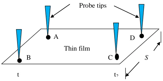
The sheet resistance (Rsh) is a measure of resistance of two dimensional film of uniform thickness. The measurement is commonly used in describing surface resistance of semiconductor materials. Four point probe set up usually consists of four equally spaced tungsten metal tips with finite radius(Pathinettam et al., 2000). Each tip is supported by springs to minimize sample damage during probing. The four metal tips are part of an auto-mechanical stage which travels up and down during measurements (Masato et al., 1993). A high impedance current source is used to supply current through the outer two probes and a voltmeter used to measure the voltage across the inner two probes. The measured voltages and sourced values of current are used to determine the sample resistivity. The units used are Ohm/sq.
The sheet resistivity of the prepared thin films was measured using the four point probe method (Agumba, 2010). This method is per Van der Pauw set up (Pathinettamet al.,2000). A symmetrical square geometry mapping of SnxSey and ZnO:Al thin films was adopted in this measurement as shown in the figure 3.4 below.Measurements were made through four contact terminals at each corner of the thin film labeled anticlockwise using a Keithley 2400 source meter.
Figure 3.4: A schematic diagram showing the arrangement used to measure sheet resistivity(Agumba, 2010).
X1 X
Distance χ refers to the length of thin film. The measurement taken were V12 and I34, V34 and I12, V23 and I14,V14 and I23 from which sheet resistance was determined using equation 3.15 below(Pathinettam et al., 2000);
R
s=
πln2
F Q
V34+V12+V23+V14
4I
Ω square
3.15where F is a function of Q given by:
𝐹 = 1 − 0.34657 𝑄−1
𝑄+1 2
− 0.09236 𝑄−1
𝑄+1 4
3.16
From V23 ≤ V42 and V23 ≥ V42 respectively;
𝑄 =
𝑉34𝑉23
𝑎𝑛𝑑 𝑄 =
𝑉23 𝑉343.17
When t << s current rings are realized and surface area A is obtained as 𝐴 = 2𝜋𝑥𝑡where
𝑥
is the radius of current ring.Sheet resistivity is calculated as follows;𝑅
𝑠= 𝜌
𝑥1𝑥2 2𝜋𝑥𝑡𝑑𝑥 3.18where t is film thickness and s is film width.
𝑅
𝑠=
𝑠2𝑠2𝜋𝑥𝑡𝜌 𝑑𝑥𝑥 3.19=
𝜌2𝜋𝑡
𝑙𝑛 𝑥 │
𝑠2𝑠=
𝜌
2𝜋𝑡
𝑙𝑛2
3.20Hence;
𝜌 =
2𝜋𝑡𝑅𝑙𝑛2 3.21
For𝑅 =2𝐼𝑉 and F being a function of Q valid for Q< 10 resistance is;
𝑅
𝑠=
𝜋𝑙𝑛2
F(Q)
𝑉3.5 I-V Characterization of thin film solar cell
A solar cell simulator was used to determine the diode characteristics of SnSe-ZnO:Al heterojunction solar cell. Figure 3.5 below shows a schematic diagram adopted in measurement of diode characteristic. When a p-n junction is under forward bias, the potential barrier is reduced resulting to increase in current through the thin film(Markvart, 1998). When under reverse bias junction potential increases. This generates small current Io (dark saturation current). Since Io is smaller than current under forward bias, the junction behaves like a diode. The I-V characteristics are given by Shockley equation as shown below (Markvart, 1998);
𝐼 = 𝐼
𝑜𝑒𝑥𝑝
𝑞𝑉𝑘𝑇
− 1
3.23where I is the current, Io is dark saturation current, V is voltage, K is Boltzmann’s constant (8.62×10⁻³ eV/K), q is the electron charge and T is the absolute temperature (373K).
Figure 3.5: Schematic diagram for measurement of diode characteristics (Sze 1981).
A p-n junction experiences equilibrium between recombination, diffusion, carrier generation, and drift in the presence of the electric field in the depletion layer if there are no external inputs(O’Leary et al., 1997).Photovoltaic (PV) cells are modeled to look like a current source in parallel with a diode. When there is no light (dark mode), the PV cell behaves like a diode. In the presence of light (light mode) current is generated by the PV cell. Current flow is basically dominated by minority carriers flowing across the junction and becoming a majority (O’Leary
etal., 1997). Figure 3.6 below shows paired electron – hole generation when a photon of sufficient energy strikes the p-n junction.
Figure 3.6: Band diagram of p-n junction solar cell showing generation of electron-hole pair due to photon absorption (O’Leary et al., 1997).
3.6P-N junction parameters
3.6.1 Short Circuit Current (ISC)
Short circuit current represents the largest amount of current which can be tapped from a p-n junction solar cell. This current is calculated when the external voltage between the external contacts is zero. The current relates to a condition when the impedance is relatively very low. For an ideal solar cell, this maximum current value is the total current produced in the solar cell by photon excitation. Isc = Imax = Ilfor forward-bias power quadrant. The short circuit current (Isc) depends on (Markvart and Casterner, 2005);
(i) Both surface area and crossectional area of the solar cell. (ii) Quantity of incoming photons.
(iv) Electrical and Optical properties of thin films.
3.6.2 Open Circuit Voltage (Voc)
The open circuit voltage (Voc) corresponds to a point on the curve when there is no current passing through the cell. It’s the highest value of voltage that can be obtained from a solar cell when the cell is operated at open circuit, 𝐼 = 0. Assuming the shunt resistance is high enough to neglect the final term of the characteristic equation, the open-circuit voltage Voc is given as(Markvart and Casterner, 2005);
3.24
The Voc depends on the rate of charge carrier recombination, percentage of doping in the window layer and saturation current in the solar cell.
3.6.3 Fill Factor (FF)
The Fill Factor (FF) is a measure of quality of solar cell and also area of the largest rectangle that will fit the I-V curve. It is calculated by comparing the maximum power (Pmax) to the theoretical power (PT) that is product of Voc and Isc. The larger the fill factor, the better the I-V characteristic curve which is more square-like. Materials which have registered good properties of solar cell candidates have a typical fill factor ranging from 0.5 to 0.82. The value of fill factor can be expressed as percentage (Markvart and Casterner, 2005); it compares the I-V characteristics of an actual photovoltaic cell to that of an ideal cell. Its value is given by equation 3.25 below(Markvart and Casterner, 2005).
𝐹𝐹 =
𝑉𝑚𝑎𝑥 𝐼𝑚𝑎𝑥𝑉𝑜𝑐𝐼𝑠𝑐 3.25
3.6.4 Efficiency (η)
The overall working of a solar cell is measured in terms of its efficiency. Efficiency refers to the comparison between energy given out (Pout) to energy taken in (Pin) into the PV cell. Pout can be taken to be Pmax since the solar cell can be operated up to its maximum power output to get the maximum efficiency(Pethe, 2004).With total radiation Pin incident on solar cell, conversion efficiency (ƞ) was calculated as shown below(Pethe, 2004);
ƞ =
𝑉𝑚𝑎𝑥 𝐼𝑚𝑎𝑥𝑃𝑖𝑛
=
𝑉𝑜𝑐𝐼𝑠𝑐𝐹𝐹
𝑃𝑖𝑛 3.26
Pindepends on area of the cell and the amount of incident photons. Its calculated as the product of the surface area of the solar cell (m2) and the irradiance of the incident light which is expressed in W/m2 or in suns (1 sun = 1000 W/m2. The maximum efficiency (ηmax) is a measure of cell performance and like all other I-V characteristics, it can be affected by the following;
(i) Temperature on the solar cell. (ii) The intensity of incident light and, (iii) Range of the incident photons.
For this reasons, it is recommended to test and compare PV cells using same temperature and lighting conditions.
3.7Thin film deposition Techniques
chemical vapours deposition, chemical reactions takes on the surface of the substrate resulting to the formation of thin films. Depending on the parameters controlled there are different types and they include Atmosphere-Pressure CVD, Metal-Organic CVD,Low-Pressure CVD and Plasma-Enhanced CVD(Ohring, 1992). Evaporation and sputtering are the two main techniques employed in physical vapour deposition. In this study, Vacuum Evaporation Technique has been adopted due to its advantages such as proper control on the substrate temperature and high deposition rate.
3.8 Physical models
3.8.1The O’ Leary-Johnson-Lim (OJL) model
Figure 3.7: Parabolic bands with tail states exponentially decaying into the band gap(Theiss, 2000).
The model gives mathematical expression for optical transition taking place between the conduction and valence bands. The fit parameters of the OJL inter band transition model are gap energy Eg, the tail state exponent of the valence band and the overall strength of the transitions. Analysis of a semiconductor material using OJL model gives fundamental parameters which reveal the optical behavior within the spectral range under study. Some of the sampled parameters are valence energy, Ev,conduction energy,Ec and their corresponding urbach damping constants valence bands, γv and conduction,γc, respectively. Masses of charge carriers within the valence band mv and conduction band mc are also included. From these parameters,the following expressions are obtained(Theiss, 2000);
C C C M E E 2 1 , 3.27 V V V M E E 2 1
, 3.28
Where Emc is the mobility edges of the conduction, Emvmobility edges of the valence band, γvvalence band damping constant and γcconduction band damping constant.From the two equations, expression for mobility gap, Eo, in the OJL model is given by(Theiss, 2000);
O V
V C
C E E
E
2 1 2
1
3.29
The value of band gap energy Eg can be obtained from a plot of density of states against energy. It’s calculated at a point where both values of conduction energy Ec and valence energy Ev are zero and its basically difference between Ec and Ev values. This energy is referred to as band gap
in the case of no disorder. Mobility band gap energy is different from band gap energy as it depends on the values of the disorder parameters Ev and Ec. The optical band energy is simulated by SCOUT 2.4 software (Theiss, 2000).
3.8.2 The Drude model
The model of electrical conduction was proposed in 1900 byPaul Drude, German physist, to explain the transport properties of electrons in a material. The model describes charge mobility especially electron transport in metals The Drude model is an application of kinetic theory which accounts for the microscopic behavior of electron in a solid. The model suggest a treatment of atom where by a heavier positive ion which is relatively immobile is surrounded by a sea of spinning electrons which are bouncing randomly. The model assumes that the metal is made of a fixed positively charged ion which is orbited by a number of “free electrons”. The interaction between the potentials of the other atoms and the valence levels makes these electrons delocalized.Regardless the origin of these free electronsfrom the contact of different potentials, the model does not consider any interference between the electrons.The model also neglects any distance interaction between the ions and electron. The only considered interaction happens within a fixed probability per unit time. The model treats both the ion and the electron as solid spheres as it’s purely classical.
The origins of alternating current and direct current conductivity, thermal conductivity and the Hall Effectin metals near room temperature within metal conductors are explicitly explained using the drude model.
A simple harmonic oscillator is a general model used when describing vibrations which are typically modelled with either fixed or massless free particles. The vibrations are considered about a certain equilibrium point. The particles considered in this case are the electrons and the heavier positive atomic nuclei. The range of resonance frequencies of these nuclei is within infrared region. Frequencies are unique as they depend on the oscillating masses and the strength of bonding between them hence can be used to classify materials a practice used in analytical chemistry(O’Learly et al., 1997).
These harmonic vibrations are useful in determination of purity of materials. Impurities such as oxygen and carbon are detected in silicondue to their characteristic vibrational modes. Harmonic oscillator is used to model electrons susceptibilities describing very small vibrations as shown below(O’Learly et al., 1997);
𝜒
𝐻𝑎𝑟𝑚𝑜𝑛𝑖𝑐 𝑜𝑠𝑐𝑖𝑙𝑙𝑎𝑡𝑜𝑟=
Ω𝑝2Ωτ02 −ṽ2−𝑖ṽΩ𝑟 3.30
where, ΩτΟis the resonance position, Ωτ the damping andΩP gives the oscillator strength. The index τo is used here since with the same oscillator model transverse optical phonons (lattice vibrations, τo -modes) are described.
3.9 Structural and elemental characterization
3.9.1 X-ray fluorescence (XRF)
sufficient energy, electrons are injected from the inner shells, creating vacancies(Bohdansky,1984). These vacancies present an unstable condition for the atom. As the atom returns to its stable condition, electrons from the outer shell are transferred to the inner shells and in the process giving off a characteristic X-ray whose energy is the difference between two biding energies of the corresponding shells. The emitted X-rays produced from this process are called “X-ray fluorescence”, or XRF. The process of detecting and analyzing the emitted x-rays is called Fluorescence spectroscopy. The technique is fast, multi-elemental, cost effective and non-destructive (Bohdansky,1984).
CHAPTER 4
MATERIALS AND METHODS
4.1 Preparation of ingots
4.1.1 Tin Selenide (SnxSey)
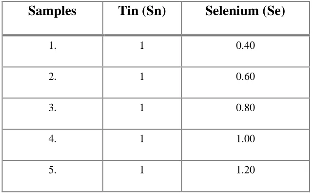
Tin and selenium which are group four and group six elements as shown in table 4.1 below were used to make the P- layer. Tin (99%) purity and selenium (99.5%) puritysamples were synthesized in specific ratios by mass ranging from 0.4 to 1.2 as shown in table 4.2. The mixer was melted in a Pyrex glass-tube in the presence of argon (Ar) gas flowing at 20sccm to avoid oxidation. The glass container was heated in an oven to a temperature of 623K until the two materials melted and mixed evenly. The heating was done continuously and gently to prevent the glass from breaking.The glass tube was completely sealed and its content allowedto cool down to room temperature (298K) before removing the mixture. The mixture was then cut into ingots that were used in the next step of thin film preparation.
Table 4.2: Tin selenide samples showing various tin to selenium ratios.
4.1.2 Aluminium doped Zinc Oxide (ZnO:Al)
Aluminum (99.99 % purity) and Zinc (99.9 % purity) were mixed at varying doping percentages of Aluminum in the range (0 – 10 %). The values of doping percentages were arrived at by calculations from the relative molecular mass of the compound.
Table 4.3: Zinc oxide sample showing various aluminium doping percentage.
Samples
Tin (Sn)
Selenium (Se)
1. 1 0.40
2. 1 0.60
3. 1 0.80
4. 1 1.00
The various samples that were made are shown in table 4.3 above.Samples were put in a silica glass tubes and then heated in presence of a constant flow of argon gas in a glass tube to form a homogenous compound.The resulting alloy was cooled naturally to room temperature forming ingots.
4.2 Evaporation and deposition SnxSey thin films
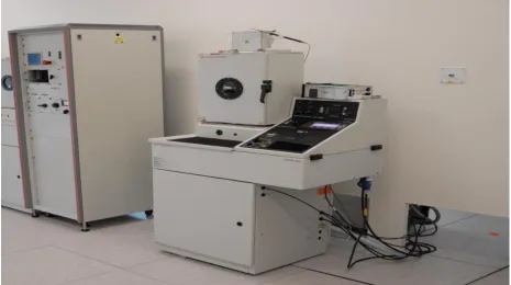
The thin films were prepared using resistive evaporation method in an Edwards vacuum deposition setup model Auto 306. The Auto 306 uses a turbo molecular pump and it’s fully automatic in its pumping procedures. The pressure is monitored using a compact gauge capable of recording atmospheric to sub-atmospheric pressure (Chapin et al.,1954).Figure 4.1 shows a photo EdwardsAuto 306 used in this study.
Sample
Al Doping Percentage
A 0%
B 2%
C 4%
D 6%
E 8%
Figure 4.1:Edwards Auto 306 coating unit.
Figure 4.2: Schematic diagram of deposition by evaporation(Drobny and Pulfrey, 1979).
4.3Evaporation and deposition of ZnO:Al thin films
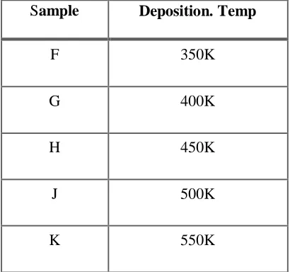
holder to attain a deposition temperature of 500K.The shutter was removed to permit deposition on glass substrate in the presence of oxygen which was let into the chamber. Since Zinc is more reactive than Aluminum, ZnO:Al thin films were formed. The Bond enthalpy of Zn-O is 159±4 kJ/mol while that of Al-O is 511±3kJ/mol (Atanas and Verka,2010). After optimizing the doping percentage, samples with an optimum value of 5% aluminium were deposited at different deposition temperature ranging from 350K-550K as shown in the table 4.4 below.
Table 4.4:Zinc oxide samples with 5% aluminium deposition temperature.
Sample Deposition. Temp
F 350K
G 400K
H 450K
J 500K
K 550K
4.4 SnSe-ZnO:Al heterojunctionFabrication
of 500 K. Finally a back contact of aluminium coat was made on the SnSe film to obtain the p-n heterojunction.
4.5 Optical measurements
Figure 4.3:The UV-VIS-NIR Spectrophotometer 3700 DUV (Shimadzu).
The spectrophotometer had two radiation sources; a deuterium lamp for UV range and a halogen lamp for visible (VIS) and near infrared (NIR) range. The radiation source changed automatically to access the wavelength range during measurements. During transmission measurements, samples were placed in front of the integration sphere and behind it during reflection measurements. SCOUT 2.4 software was used to simulate transmittance data to get the optical constants like absorption coefficient among others. Drude, OJL and Harmonic Oscillator models were used to simulate the data. These models are inbuilt in the SCOUT 2.4 software (Theiss, 2000). The models simulate refractive index, dielectric function, absorption coefficient real and imaginary parts and energy loss parameters.
4.6 Sheet resistivity measurements
experimental set up used to obtain the resistivity data. With a symmetrical square geometry adopted, the four leads from the probe head were connected to Keithley SourceMeter via relay switching circuit as per the Van der Pauw set-up for Voltage and Current measurements (Agumba, 2010).
Figure 4.4:Keithley 2400 source meter for measurement of sheet resistance.
The four probes were lightly pressed on the sample as shown in figure 4.5 below to avoid damaging the film.
Figure 4.5: Schematic diagram of a four point probe used to measure surface sheet resistivity (Brown and Jakeman, 1996).
A D
C B
Thin film sample
Probe tips
t
1
t2
4.7 Rapid Thermal Processing
Rapid Thermal processing (RTP) is a technique used widely in semiconductors processing where there are thermal constraints. The annealing system used in this work was Nabertherm Programmable Furnace system whose photograph is shown in figure 4.6 below. A schematic representation of the annealing chamber is shown in figure 4.7 below. The furnace consist a chamber surrounded by heating elements on the four sides. The samples are placed on hearth plates and heated radiatively at their top surface and conductively at their bottom surface. A process gas is continuously flowed through the sample chamber. The fan ensures even distribution of heat to the samples. The fiber muffle ensures the heat is contained within the chamber.
CHAPTER 5
RESULTS AND DISCUSSION
5.1 Optical characteristics of ZnO:Al 5.1.1 Optical spectra of ZnO:Althin films
The optical transmittance spectra of ZnO:Al films as a function of wavelength in the range (300 - 1200 nm) were plotted. Figure 5.1 shows different spectra for films with differentaluminium doping percentages.
Figure5.1:Graph oftransmittancespectra of ZnO:Al films.
High values of transmittance ranging from 60 % to 90 % were obtained as shown in the figure above. Transmittance increased steadily to a maximum value before remaining constant as the wavelength increases for all the samples.This can be attributed to minimal optical absorption taking place as the energies of the incoming photons are lower than the band gap energy of the
200 400 600 800 1000 1200
thin films. As the doping percentage was increased beyond 5%, there was a slight decrease in transmittance. This is due to excess free carriers coupling to the electric field hence increasing the reflection.This agrees very well with Elmin et al.(2009) who reported significantly reduced transmission when ZnO was doped with higher percentages of Aluminum. Average transmittance for different spectrum region was calculated and a high transmittance of 80.76% was recorded in the visible region as shown in table 5.1 below.
Table 5.1: Average transmittance of ZnO:Alwithin different spectrum regions.
percentage of Aluminum in thesample
Average
transmittance in ultra violetregion (300-400nm)
Average
transmittance in visible region (401-750nm)
Average
transmittance in near infrared region (751-1000nm)
0 37.09 63.30 72.27
2 62.31 78.44 76.25
4 63.64 80.76 77.29
6 65.83 79.66 76.95
8 45.42 70.86 74.55
10 37.80 63.92 72.35
0 2 4 6 8 10 64 68 72 76 80 Tr an sm itt an ce (% )
Al doping percentages
Figure 5.2: Graph of average transmittance in ZnO:Alwithin the visible region.
Figure5.3:Graph ofreflectancespectra of ZnO:Al films due to doping.
Very low values reflectanceranging from 4% to 9% in the ultra violet, visible range and infra-red was recorded. Figure 5.3 above shows the nature of spectra scatteinfra-red from the reflectance data. The kinks observed in the spectra was due to spectrophotometer changing radiation
200 400 600 800 1000 1200
sourcefrom either a halogen lamp for visible (VIS) and near infrared (NIR) range or a deuterium lamp for UV range. This occurs automatically in order to access the wavelength range during measurementsas deposition temperature was increased.
200 400 600 800 1000 1200
0 20 40 60 80 100 Deposition Temp. 350K 400K 450K 500K 550K T ra n sm it ta n c e ( % ) wavelength (nm)
Figure5.4:Graph ofreflectancespectra of ZnO:Al films due to deposition temperature.
5.1.2 Thickness of thin films
The figure 5.5 below shows variation of film thickness (nm) with increase in deposition temperature. The thickness decreased exponentially as there was a high rate of re-evaporation at high deposition temperature on the glass substrate.
350 400 450 500 550
104 106 108 110 112 114 116
Thickness
T
hi
ck
ne
ss
(
nm
)
Deposition Temperature (K)
Figure5.5:Graph offilm thickness with deposition temperature.
5.1.3Simulated and experimental Graph
The experimental and background data of the material from the scout software were plotted against wavelength for samples with 5% aluminium doping. The simulated curve fitted perfectly into the experimental curve as shown in figures 5.6 below.
200 400 600 800 1000 1200
0 20 40 60 80 100
Experimental
Simulated
T
rans
m
itt
anc
e
(%)
Wavelength (nm)
Figure5.6: Simulatedand experimental graphfor 5% aluminium doped ZnO.
5.1.4 Optical bandgap energies
increased beyond five percentages, there was slight decrease in band gap energy. This can be attributed to creation of new donor levels above the valence band.
Table 5.2:ZnO doped with aluminiumand calculated bandgap energyvalues.
Percentage of Aluminium in ZnO Band gap energy (eV) Band gap error (eV)
0 3.17 0.050
2 3.35 0.052
4 3.60 0.057
6 3.54 0.062
8 3.38 0.059
By use of Gaussian amplified peak function, doping percentage was optimized at 5% aluminium doping as shown in figure 5.7 below with a band gap of 3.60eV. This value falls within the range of 3.28-4.20±0.05 eV reported by Mugah(2011).
0 2 4 6 8
3.1 3.2 3.3 3.4 3.5 3.6 3.7
B
an
d
ga
p
en
er
gy
(e
V
)
Doping concetration (%)
5.2 Optical characteristics of SnSe
5.2.1 Transmittance data against wavelength
The transmittance of all synthesized ratios of tin selenide was observed to be below 40% as shown in figure 5.8 below. The values agree with a transmittance of below 45% reported by Kioko (2011). It is observed that there is variation in transmittance within the visible region due to variation in selenium ratio. There was a slight decrease in transmittance for wavelengths above 600nm. This can be attributed to increase in optical scattering caused by rough surface morphology. The ratio of 1:1 gave the lowest transmittance in the visible region. This makes the material suitable candidate for application as absorber electrode for solar cell.
200 400 600 800 1000 1200
0 10 20 30 40 50
T
ra
n
sm
it
ta
n
ce
(
%
)
Wavelength (nm)Sn:Se
1:0.4
1:0.6
1:0.8
1:1.0
1:1.2
5.2.2 Transmittance, Reflectance and Absorbance averages in the visible region
The values of absorbance in the visible region were noted to be above 50% as shown in figure 5.9 below. There was a slight increase in absorbance as the ratio of selenium was increased in the mixture. Much of the incoming photons have energies comparable with the band gap of the material. This leads to an increase in absorption. A ratio of 1:1 gave a higher absorbance of 58.93% in this region of spectrum. This value was used as optimum synthesis ratio in the fabrication of the p-n solar cell junction.
0.4
0.6
0.8
1.0
1.2
0
10
20
30
40
50
60
P
e
rc
e
n
ta
g
e
(
%
)
Ratio Se/Sn
Absorbance
Reflectance
Transmittance
5.2.3 Simulated and experimental Graph
The simulated and background data of the material from the scout software were plotted against wavelength for samples with ratio of Tin to Selenium as 1:1. The simulated curve fitted perfectly into the experimental curve as shown in figures 5.10 below.
200 400 600 800 1000 1200
0 5 10 15 20 25 30 35 40
T
rans
m
itt
anc
e
(%)
Wavelength (nm)
Experimental
Simulated
Figure5.10: Simulatedand experimental graphfor Tin selenide at a ratio of 1:1.
5.2.4 Optical bandgap energies
absorption of incoming photons takes place at the top of the valence band. Excited photons have sufficient energy to overcome the potential barrier due to forbidden zone and cross over to the bottomof the conduction band. SnSe thin films exhibit direct optical energy band gap. Obtained values are in good agreement with the band gap value range of 1.18 and 1.85±0.05 eV as reported by Kumar etal. (2010).
Table 5.3:Band gap energy values and ratios of Se/Sn by mass.
Ratio of Se/Sn Optical band gap (eV) Band gap error
0.4 1.73 0.030
0.6 1.66 0.034
0.8 1.47 0.034
1.0 1.37 0.024
1.2 1.39 0.043
Fromtheresults,agraphofopticalbandgapenergy versusSe/Snsampleratioswasdrawn. ThevariationingraphshowsthattheoptimumSn:Sethinfilmratiovalueisthatof1:1
0.4 0.6 0.8 1.0 1.2 1.3 1.4 1.5 1.6 1.7 1.8 B a n d g a p e n e rg y ( e V )
Ratio of Se/Sn
Figure 5.11: Graph of variation of optical band gap energy with different Sn:Se ratios.
5.2.5 Refractive index
Refractive index values of SnxSey samples were plotted against wavelength as shown below.
200 400 600 800 1000 1200 1.90 1.95 2.00 2.05 2.10 2.15 2.20 Ratio Se/Sn 0.4 0.6 0.8 1.0 1.2 R ef ra ct iv e in d ex , (n ) Wavelength (nm)
Figure 5.12 aboveshowsthatthe refractive indicesof thethinfilmsremain fairly constantasthewavelengthincreases.Thismustbe relatedtothe complexreflectance behavior onthe surface of thedepositedthinfilms.Thisisattributedtospectroscopic ellipsometry theory;whichdefinestheabilitytoreportrealrefractiveindexofthinfilmsover awide rangeof wavelength values.
5.2.6 Absorption coefficient for tin selenide
Absorption coefficient for tin selenide at different ratios was plotted against wavelength from 300nm to 1200nm. High absorption coefficient at lower wavelength was realized for all samples with Sn:Se as ratio of 1:1 recording the highest as shown in figure 5.13 below. For all samples, tin selenide had a high absorption coefficient within the visible range (380-750nm) with an average absorption of more than 2.0 × 105 cm-1 thus making it a reliable material for forming a good absorber layer for solar cells. (Porortmans and Arkhipov, 2006).
200 400 600 800 1000 1200
-5.0x10⁵ 0.0 5.0x10⁵ 1.0x10⁶ 1.5x10⁶ 2.0x10⁶ 2.5x10⁶ A b so rp ti o n c o ef fi ci en t (c m -1 ) Wavelength (nm) Ratio Se/Sn 0.4 0.6 0.8 1.0 1.2
5.3 Optimized deposition parameters of ZnO:Aland SnxSey thin films
Table 5.4 below gives the optimized depositionparameters fordifferent doped concentrations ofZnO:Althin films andvariedsynthesized ratios of SnxSey. These parameters were used in the fabrication of PN junction solar cell.
Table 5.4:Optimized deposition parameters forZnO:Al and SnxSeythin films.
ZnO:Al SnxSey
Optimized deposition
temperature 510K Deposition temperature 500K
Doping concentration 5.0% Optimized ratio 1:1
Deposition pressure 3.5×10⁻⁵ mb Deposition pressure 3.5×10⁻⁵ mb
Oxygen flow rate 20sccm Heater current 3.5A
5.4 Electrical characterizationofZnO:Al and SnSethin films
5.4.1 ZnO:Al thin film
substitutional sites of Zn2+ ions. This creates an extra free charge carrier in the film. Majority of aluminiumionsintroducedin the crystal lattice replaces the Zn2+ ions resulting in increased charge carriers, hence high conductivity (Mudjat et al., 2008). Low resistivity valuesfor ZnO:Al thin film is also associated with the difference in Hall mobility that measures the average carrier density in a grain.
At lower substrate heating the films shows an incompletereaction and films with rough surface are obtained. Thesefilmshave anonstoichiometric structure, which produces a low resistivity structure due to the oxygen vacancies and interstitialzinc atoms acting as donors hence giving rise to highercarrier concentration and Hall mobility (Dong-Joo Kwaketal., 2004). However, there is steady increase in resistivity at substrate temperature above 510K. This is due to active promotion of oxidation onthe film surface and a decrease in deposition rate dueto a re-evaporation of film at higher substrate heating.
350 400 450 500 550
2.9 3.0 3.1 3.2 3.3 3.4
Deposition Temperature (K) Resistivity
conductivity
Figure 5.14: Graph of resistivity and conductivity as a function of deposition temperature.
Conductivit y ((σ) x 10
-2
[Ω-cm]-1
5.4.2 SnSethinfilm
The sheet resistivity values for the SnSe thin film ranged from 22.95 Ωcm - 24.75 Ωcm.A sample with ratio of 1:1 recorded the lowest resistivity as shown in figure 5.15 below. The sheet resistivity for 1500C annealed thin film was 19.26±0.05 Ωcm. This low resistivity is due to high carrier mobility and carrier concentration associated with the films. Deposition conditions such as current, deposition temperature and pressure may also have contributed to low resistivity by modifying the thin film surface morphology hence affecting its binding properties (Sharma et al., 2005).
0.4 0.6 0.8 1.0 1.2
25 30 35 40 45
Tin-Selenium Ratio Resistivity
Conductivity
Figure 5.15: Graph of resistivity and conductivity as a function of tin–selenium ratio.
A lower resistance value for annealed film at 1500C with argon flowing at a rate of 5sccm for 30 minutes was obtained as compared to the unannealed thin film. This indicates that annealing promotes incipient fusion of small crystallites and thereby reduces the grain boundaries, which are known to act as recombination centers for minority carriers and trapping centers for majority carriers. This physical change on the surface of the thin films affected the binding properties of
Resistivity (ρ)[Ω-cm]
Conductivity
(σ)x 10-3
[Ω-cm]