Design and Anaysis of Shift Register Using Pulse
Triggered Latches
Manthri Lavanya
& D.Sreekanth Reddy
1
M.Tech ,Assistant Professor, Department of ECE, Anantha Lakshmi Institute of Technology,
Anantapur, Ap, India.
2
M.Tech ,Assistant Professor, Department of ECE , Srinivasa Ramanujan Institute of Technology,
Anantapur, Ap, India.
ABSTRACT- The most recent headway in register
innovation is to keep up low region and low power utilization. Shift register is a computerized memory circuit. The Shift register is made out of flip-flop having a similar check in which the yield of each associated with information contribution of next flip-flop in the chain and have no circuit between the flops. Master slave flip-flop is course of two latches. Size is more for the plan of long length and power utilization is high. Shift register created by pulse latch comprising of a latch and a pulse clock flag. By utilizing pulse latch as a part of shift register, timing issue will happen. Keeping in mind the end goal to defeat the planning issue postpone circuits must be presented; yield flag of the latch is deferred and achieves the following hook after the clock beat. At that point all latches have consistent info signals amid the clock; the postpone circuits cause vast territory and power overheads. The arrangement is to utilize different non cover deferred pulse clock signals. Every latch utilizes a pulse clock flag which is deferred from the beat check flag utilized as a part of its next latch. Subsequently, every latch upgrades the information after its next latch overhauls the information. Every latch has a consistent contribution amid its clock beat and no planning issue happens between latches, power and zone are spared. A shift register can likewise be utilized as a counter. A shift register with the serial yield associated back to the serial info is called shift register counter. In
light of such an association, uncommon determined successions are created as the yield. The most well-known shift register counter is Johnson counter. Supplanting flip-flops with pulse latches in the plan of counter will lessen territory and power. Johnson counter can be planned by utilizing pulse latch.
Index terms – flip-flop, Pulse latch, pulse clock, shift register
I INTRODUCTION
applications, because a pulsed latch is much smaller than a flip-flop. The area and power will be reduced by using pulsed latches in the design of shift register. No single existing design performs well across the wide range of operating regimes present in complex systems. The use of a selection of flip-flop and latch designs, are proposed for different activation patterns and speed requirements. A master-slave flip-flop using two latches in figure 1(a) can be replaced by a pulsed latch consisting of a latch and a pulsed clock signal in figure 1(b). All pulsed latches share the pulse generation circuit for the pulsed clock signal. As a result, the area and power consumption of the pulsed latch become almost half of those of the master-slave flip-flop. The pulsed latch is an attractive solution for small area and low power consumption.
Fig:1. (a) Master-slave flip-flop. (b) Pulsed latch.
A shift register can also be used as a counter. A shift register with the serial output connected back to the serial input is called shift register counter. Because of such a connection, special specified sequences are produced as the output. The most common shift register counter is Johnson counter. Replacing flip-flops with pulsed latches in the design of counter will reduce area and power. Johnson counter can be designed by using pulsed latches.
II EXISTING SYSTEM
Shift registers are specialized memory systems composed of flip-flops or other types of memory cells. The distinguishing feature of shift registers is that data can be transferred on command from one cell to the adjacent memory cell as many times as needed. The
Fig: 2 Schematic of the PPCFF
PPCFF contains four PMOS transistors, four NMOS transistors and two transmission gates, two inverters. The architecture of a shift register is quite simple. An N-bit shift register is composed of series connected N data flip-flops. The speed of the flip-flop is less important than the area and power consumption because there is no circuit between flops in the shift register. The smallest flip-flop is suitable for the shift register to reduce the area and power consumption. The shift register which is designed by flip-flop occupies more area, power consumption and dissipation and complexity of the circuitry is also high in design of high range bit of shift register will become more complex.
III PROPOSED SYSTEM
(a) Schematic
(b)Waveforms
Fig: 3 Shift register with latches and a pulsed clock signal. (a) Schematic. (b) Waveforms.
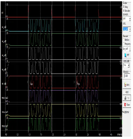
Flip-flops are used to design a shift register. By replacing flips-slops with latches in the designing of shift register area and power will be saved. So power and area will become less. The pulsed latch cannot be used in shift registers due to the timing problem, as shown in Figure 3. The shift register in Figure 3(a) consists of several latches and a pulsed clock signal (CLK_pulse). The operation waveforms in Figure 3(b) show the timing problem in the shift register. The output signal of the first latch (Q1) changes correctly because the inputs signal of the first latch (IN) is constant during the clock pulse width. But the second latch has an uncertain output signal (Q2) because its input signal (Q1) changes during the clock pulse width.
One solution for the timing problem is to add delay circuits between latches, as shown in Figure 4(a). The output signal of the latch is delayed and reaches the next latch after the clock pulse. As shown in Figure 4(b) the output signals of the first and second latches (Q1 and Q2) change during the clock pulse width , but the input signals of the second and third latches (D2 and D3) become the same as the output signals of the first and second latches (Q1 and Q2) after the clock pulse. As a result, all latches have constant input signals during the clock.
(b) Waveforms
Fig:4 Shift register with latches, delay circuits, and a pulsed clock signal. (a) Schematic. (b) Waveforms.
Another solution is to use multiple non-overlap delayed pulsed clock signals, as shown in Figure 5. The delayed pulsed clock signals are generated when a pulsed clock signal goes through delay circuits. Each latch uses a pulsed clock signal which is delayed from the pulsed clock signal used in its next latch. Therefore, each latch updates the data after its next latch updates the data. As a result, each latch has a constant input during its clock pulse and no timing problem occurs between latches. However, this solution also requires many delay circuits. The delay circuits cause large area and power overheads.
(a)Schematic
(b)wave forms
Fig: 5 Shift register with latches and delayed pulsed clock signals. (a) Schematic (b) Waveforms
Figure 6 shows the proposed shift register. The proposed shift register is divided into M sub shifter registers to reduce the number of delayed pulsed clock signals. A 4-bit sub shifter register consists of five latches and it performs shift operations with five non-overlap delayed pulsed clock signals (Clock pulse [1:4] and Clock pulse [T]).
Fig: 6 shift register
To get delay in clock pulses delayed pulsed clock generator is used. Delayed pulsed clock generator is shown in figure 7. Delayed pulse clock generator consisting clock pulse circuits. All clock pulse circuits connected in cascade fashion. Each clock pulse circuit contains a delay circuit, inverter, AND gate and buffer. The conventional delayed pulsed clock circuits in Figure 7 can be used to save the AND gates in the delayed pulsed clock generator in Figure 7. In the conventional delayed pulsed clock circuits, the clock pulse width must be larger than the summation of the rising and falling times in all inverters in the delay circuits to keep the shape of the pulsed clock. However, in the delayed pulsed clock generator in Figure 7 the clock pulsed width can be shorter than the summation of the rising and falling times because each sharp pulsed clock signal is generated from an AND gate and two delayed signals. Therefore, the delayed pulsed clock generator is suitable for short pulsed clock signals.
Fig: 7 Delayed pulse clock generator
IV PULSED LATCH APPROACH
Low power has emerged as a principal theme in today’s world of electronics industries. Power dissipation has become an important consideration as performance and area for VLSI Chip design. With shrinking technology reducing power consumption and over all power management on chip are the key challenges below 100nm due to increased complexity. For many designs, optimization of power is important as timing due to the need to reduce package cost and extended battery life. For power management leakage current also plays an important role in low power VLSI designs. A latch can capture data during the sensitive time determined by the width of clock waveform. Pulsed latch structures employ an edge-triggered pulse generator to provide a short transparency window. If the pulse clock waveform triggers a latch, the latch is synchronized with the clock similarly to edge-triggered flip-flop because the rising and falling edges of the pulse clock are almost identical in terms of timing.
generators that generate pulse clock waveforms with a source clock. The pulse width is chosen such that it facilitates the transition. Pulse generators can be shared among a few latch cells to reduce energy, if care is taken that the pulse shape does not degrade due to wire delay, signal coupling and noise. We measured designs both with individual pulse generators and with pulse generators shared among four latch bits, in which case we divide the pulse generator energy among the four latch instances.
Fig: 8 Schematic of SSASPL
In chip implementation, the SSASPL (static differential sense amp shared pulse latch) is selected which is the smallest latch. SSAPL is a pulsed version of SSALA with individual pulse generators, while SSASPL has a shared pulse generator.
The two series transistors in SSAPL are replaced by a single transistor in SSASPL. The original SSASPL with 9 transistors is modified to the SSASPL with 7 transistors in Figure 8 by removing an inverter to generate the complementary data input (Db) from the data input (D). In the proposed shift register, the differential data inputs (D and Db) of the latch come from the differential data outputs (Q and Qb) of the previous latch. The SSASPL uses the smallest number of transistors (7 transistors) and
it consumes the lowest clock power because it has a single transistor driven by the pulsed clock signal. The SSASPL updates the data with three NMOS transistors and it holds the data with four transistors in two cross-coupled inverters.
It requires two differential data inputs (D and Db) and a pulsed clock signal. When the pulsed clock signal is high, its data is updated. The node Q or Qb is pulled down to ground according to the input data (D and Db). The pull-down current of the NMOS transistors must be larger than the pull-up current of the PMOS transistors in the inverters.
V COUNTER
A shift register can also be used as counter. The output of the last shift register is fed to the input of the first register.. A twisted ring counter also called switch-tail ring counter connects the complement of the output of the last shift register to the input of the first register and circulates a stream of ones followed by zeros around the ring. For example, in a 4-register counter, with initial register values of 0000, the repeating pattern is: 0000, 1000, 1100, 1110, 1111, 0111, 0011, 0001, 0000. A Johnson counter is a ring with an inversion; a 4-bit Johnson counter is shown in figure 9. Note the inversion of the Q signal from the last shift register before feeding back to the first D input, making this a Johnson counter. This arrangement produces a unique sequence of states. Initially, the register is cleared. So all the outputs are zero.
are zero. Counter uses a shift register which is composed of pulsed latches in order to reduce area and power consumption.
Fig: 9 Johnson ring counter
VI RESULTS
A. SCHEMATIC OF SSASPL
Fig: 10 schematic of SSASPL
The Schematic diagram of SSASPL (static differential sense amp shared pulse latch) is shown in the figure 10 consists three NMOS transistors and two cross-coupled inverters.
B. LAYOUT OF SSASPL
Fig: 11 layout of SSASPL
From this layout power of SSASPL 4.948µw. C. POWER REPORT OF SSASPL
Fig: 12 power report of SSASPL
D. SCHEMATIC OF SHIFT REGISTER
Fig: 13 Shift register schematic
The proposed systems of schematic diagram consist of pulsed clock generator and 4-bit sub shift registers. Schematic of shift register with latches is shown in the figure.
E. SCHEMATIC OF SHIFT REGISTER WITH PULSED LATCHES (SSASPL)
Fig: 14 schematic of shift register with pulsed latches (SSASPL)
Internal schematic of shift register is shown in the figure. Shift register designed with the pulsed latches. SSASPL (Static differential Sense Amp Shared pulsed latch) has 7 transistors.
F. POWER REPORT OF SHIFT REGISTER
0.827mw. Power report of shift register is shown in figure.
Fig: 15 power report of shift register
G. SCHEMATIC OF JOHNSON COUNTER
Figure shows the schematic of 4-bit Johnson counter and it contains four latches. Four latches connected in cascade fashion. Output of last latch inverted and feedback to the first latch. Input clock signal is given to all four latches.
Fig: 16 schematic of Johnson counter
H. LAYOUT OF JOHNSON COUNTER
Layout of Johnson Counter is shown in figure 28. From this layout power of counter can be estimated. Power of counter is 0.269mw.
I. POWER REPORT OF COUNTER
Power report of Johnson counter is shown in the figure. By running layout of the Johnson counter power will be evolved. Power consumption of Johnson counter is 0.269mw.
Fig: 18 power report of Johnson Counter
VII CONCLUSION
The shift registers, counters reduce area and power consumption by replacing flip-flops with pulsed latches. The timing problem between pulsed latches is solved by using multiple non-overlap delayed pulsed clock signals instead of a single pulsed clock signal. A small number of the pulsed clock signals are used by grouping the latches to several sub shifter registers and using additional temporary storage latches. Any number of bits shift registers can be developed.
VIII REFERENCES
[1] P. Reyes, P. Reviriego, J. A. Maestro, and O. Ruano, “New protection techniques against SEUs for moving average filters in a radiation environment,” IEEE Trans. Nucl. Sci., vol. 54, no. 4, pp. 957–964, Aug. 2007. [2] M. Hatamian et al., “Design considerations for gigabit ethernet 1000 base-T twisted pair transceivers,” Proc. IEEE Custom Integr. Circuits Conf., pp. 335–342, 1998. [3] H. Yamasaki and T. Shibata, “A real-time imagefeature-extraction andvector-generation vlsi employing arrayed-shift-register architecture,” IEEE J. Solid-State Circuits, vol. 42, no. 9, pp. 2046–2053, Sep. 2007.
[4] H.-S. Kim, J.-H. Yang, S.-H. Park, S.-T. Ryu, and G.-H. Cho, “A 10-bitcolumn-driver IC with parasitic-insensitive iterative charge-sharing based capacitor-string interpolation for mobile active-matrix LCDs,” IEEE J. Solid-State Circuits, vol. 49, no. 3, pp. 766–782, Mar. 2014.
[5] S.-H. W. Chiang and S. Kleinfelder, “Scaling and design of a 16-megapixelCMOS image sensor for electron ,microscopy,” in Proc. IEEE Nucl. Sci. Symp. Conf. Record (NSS/MIC), 2009, pp. 1249–1256.
[6] S. Heo, R. Krashinsky, and K. Asanovic, “Activitysensitive flip-flopand latch selection for reduced energy,” IEEE Trans. Very Large Scale Integr. (VLSI) Syst., vol. 15, no. 9, pp. 1060–1064, Sep. 2007.
[7] S. Naffziger and G. Hammond, “The implementation of the nextgeneration 64 b itanium microprocessor,” in IEEE Int. Solid-State Circuits Conf. (ISSCC) Dig. Tech. Papers, Feb. 2002, pp. 276–504.