A NEW REDUCED SIZE MICROSTRIP PATCH ANTENNA WITH FRACTAL SHAPED DEFECTS A. Kordzadeh and F. Hojat Kashani
College of Electrical Engineering
Iran University of Science and Technology Narmak, Tehran, Iran
Abstract—With development of communication with integration technology, size reduction of microstrip antennas is becoming an important design consideration for practical applications. Here a new microstrip antenna with Koch shaped fractal defects on the patch surface is presented. Using this method, the overall electric length of the antenna is increased largely and hence the size of antenna is reduced to 85%, compared to an ordinary microstrip antenna with the same resonance frequency. Antenna is simulated using high frequency structure simulator (HFSS) V.10 which is based on finite element modeling (FEM). Finally antenna is fabricated on RO4003 substrate. Measurement results are in good agreement with simulated results.
1. INTRODUCTION
that are embedded on the antenna are used to increase the surface current path. To decrease the resonant frequency of an antenna for a given surface area, the current path must be maximized within the area [4].
Fractal shaped antennas showsome interesting features which results from their geometrical properties. These shapes are characterized by two important properties; one of them is self similarity and another one is space filling. The self-similarity of certain fractal structures result in a multi-band behavior of self similar fractal antennas and frequency selective surfaces (FSS) [5]. Due to their space filling prosperities, Fractals can be used in antenna miniaturization. The usage of space filling curves increase antenna’s electrical length [6].
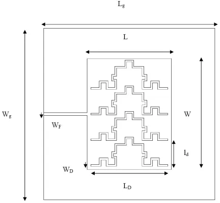
Figure 1. Schematic of the antenna.
2. ANTENNA GEOMETRY AND OPERATION MECHANISM
radiating edge. Four fractal defected microstrip structures (DMS) are excoriated from the patch’s surface. The lengths of these DMS’s are Ld and their width are Wd, and all have the same dimensions. These DMS’s are placed at equal distances from each other. Table 1 shows the designed dimensions that are used for the antenna.
Table 1. Designed dimensions of the antenna in mm.
Wg Lg W L WD LD ld Wf
100 100 65 49 1 45 15 1.7
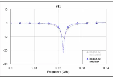
The proposed antenna is simulated using high frequency structure simulator (HFSS) V.10 which is based on finite element modeling (FEM). Fig. 2 shows the simulated and measured return loss versus frequency for the proposed antenna without matching network. As it can be seen in this figure, the first resonance occurs at 622 MHz, in comparison with the antenna with the equal size but without DMS’s that has a resonance frequency at 1.61 GHz. A rectangular patch with the resonance frequency at 622 MHz, must have a total area of about 31353 mm2. The proposed antenna with the total area of 3204 mm2, operates at this frequency. So the size reduction of this approach is about 85% in comparison with ordinary patch.
Figure 2. Simulated and measured return loss of the proposed structure.
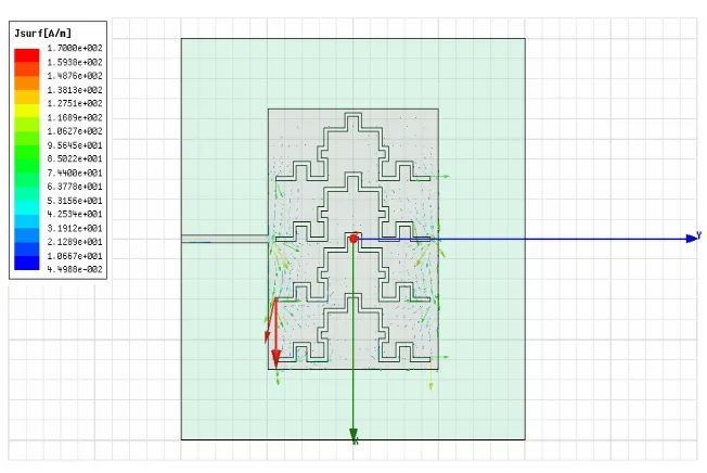
Figure 3. Simulated vector surface current distribution on the patch antenna.
is meandered and hence the electrical length of antenna is increased, although the physical length is left constant. So by increasing the electrical length of the antenna, the resonance frequency is decreased. This means that for an antenna with the same resonance frequency, the overall surface of antenna is decreased to a great amount.
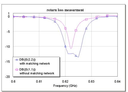
The simulated antenna impedance bandwidth for 10 dB return loss is very narrow(below1%). In order to increase the antenna bandwidth to an acceptable value, a matching circuit, as shown in Fig. 4, is used at the feed line, to achieve a higher bandwidth. This matching circuit is simulated and optimized by Microwave Office 2004 (AWR V.6.51). These LC matching circuit parameters are optimized in order to achieve an acceptable bandwidth about 1%. The final optimized values are inserted at the antenna feed line, and are listed on Table 2.
Table 2. Values of optimized parameters of the matching network.
L1 L2 C1 C2
8.2 nH 56 nH 28.8µF 10.14µF
Figure 4. Matching network.
Figure 5. Measured return loss of the proposed antenna with and without matching circuit.
antenna with and without matching network. It can be seen that bandwidth is increased to 1%.
3. MEASUREMENT RESULTS
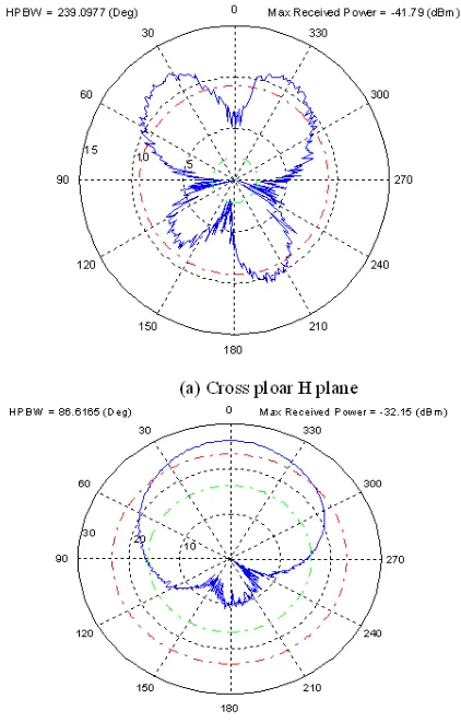
Figure 7. The measured radiation pattern.
4. THE EFFECT OF DIMENSIONAL VARIATION ON FREQUENCY RESPONSE
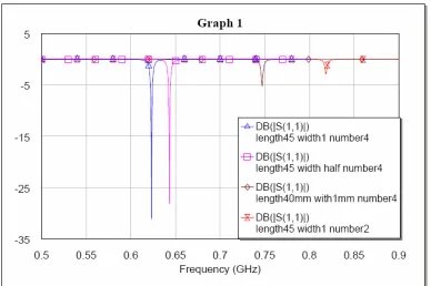
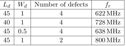
As shown in previous sections, by inserting several DMS’s on the patch antenna, the resonant frequency is decreased. In this section, the effect of these defects’ dimensions such as their length and width, on the frequency response is investigated. By increasing defect’s length, the electrical length is increased more; hence there is a more reduction in the resonant frequency. These effects are more obvious in Fig. 8. In this figure once the element length is fixed and width is halved, and once length is decreased and width is remained fixed and in another one, number of defects is reduced to 2. In this figure, length and width is related to the defects dimensions, and number refers to the number of defects. Table 3 list values and their related resonant frequency that are used for this analysis. As is expected, higher number of these defects results in more increase in electrical length and more decrease in the resonance frequency.
Table 3. Effects of dimensional variations of the DMS on the resonance frequency.
Ld Wd Number of defects fr
45 1 4 622 MHz
40 1 4 728 MHz
45 0.5 4 638 MHz
45 1 2 800 MHz
5. CONCLUSION
REFERENCES
1. Lo, T. K. and Y. Hwang, “Microstrip antennas of very high permittivity for personal communications,” 1997 Asia Pacific Microwave Conference, 253–256, 1997.
2. Sinati, R. A., CAD of Microstrip Antennas for Wireless Applications, Artech House, Norwood, MA, 1996.
3. Wang, H. Y. and M. J. Lancaster, “Aperture-coupled thin-film superconducting meander antennas,” IEEE Transaction on Antennas and Propagation, Vol. 47, 829–836, 1999.
4. Waterhouse, R., Printed Antennas for Wireless Communications, John Wiley & Sons Inc, 2007.
5. Borja, C. and J. Romeu, “On the behaviour of koch island fractal boundry microstrip patch anetnna,”IEEE Transaction on Antennas and Propagation, Vol. 51, No. 6. July 2003.