Design of Compact Wideband High-Selectivity Band-Stop Filter
Based on Coupled Lines
Menglou Rao, Yongle Wu*, Weimin Wang, and Yuanan Liu
Abstract—In this paper, a compact band-stop filter with a wideband and high-selectivity performance is proposed and analyzed. This band-stop filter includes two parallel-coupled lines of different electrical lengths and two open-circuit stubs. A lossless transmission line model is used to obtain the filter design parameters. In order to verify this new filter circuit structure and its corresponding design theory, five groups of numerical examples are demonstrated. Finally, a practical band-stop filter with a 3-dB cutoff frequency bandwidth of 58.2% centered at 0.94 GHz has been designed, simulated and measured. The measured results show a good agreement with the simulated responses.
1. INTRODUCTION
Wideband band-stop filters are in increasing demand in microwave circuit applications to suppress undesired wideband signals. The conventional microstrip band-stop filter [1] has open-circuited stubs and shunt stubs of a quarter-wavelength. However, the bandwidth of this filter is narrow and the upper band-stop center frequency is located at three times of the operating center frequency in the fundamental stopband. To meet the requirement of low insertion loss and sharp rejection, various structures and bandwidth enhancement technologies for band-stop filters have been developed in recent years [2–9]. For example, a compact band-stop filter using Defected Microstrip Structure (DMS) by etching Open Square Ring (OSR) is proposed in [2], which has low insertion loss in the passband and high rejection level. The T-shaped defected microstrip structures and the U-shaped defected ground structures are provided to create a novel miniaturized dual-band band-stop filter in [3]. Meanwhile, modified stubs are also applied to construct wideband band-stop filters in [4]. Coupled lines have been widely used for implementing filters for a long time. It can improve the upper pass-band performance in band-stop filters [5] and sharpen skirt selectivity of filters [6]. A compact microstrip coupled-line configuration has been presented to design an ultra-wideband band-stop filter in [7]. The band-stop filter presented in [8] also uses two symmetrical coupled-line stubs to form two shorted points to realize dual-stopband characteristics, which can work with low insertion loss in the passband and sharp rejection in the stopbands. In [9], a microstrip band-stop filter using two meandered parallel-coupled lines of different electrical lengths and characteristic impedances in shunt is presented. Yet, note that this band-stop filter has two obvious disadvantages: low selectivity and poor return loss in passband.
In order to remove these two limitations, a modified filter is discussed and proposed in this paper. Extended from the band-stop filter in [9], two open-circuit stubs are added symmetrically, thus this proposed structure is symmetrical. This improved circuit configuration has a higher selectivity, better return loss and lower insertion loss for passband. The total external performances can be expressed by closed-form mathematical expressions. The performance of this band-stop filter can be controlled by different even- and odd-mode characteristic impedances of the coupled lines and the characteristic impedances of the open-circuit stubs. To illustrate the effects of different kinds of impedance values, five parts of discussion are represented. According to the analysis, two types of ideal band-stop filters
Received 18 July 2014, Accepted 10 August 2014, Scheduled 23 August 2014
* Corresponding author: Yongle Wu ([email protected]).
with normal operating frequency (1 GHz) are designed, calculated and discussed by using lossless transmission-line and coupled-line models. Afterwards, the band-stop filter operating at 1 GHz has been simulated with a full-wave simulation tool. To verify the theoretical prediction, the filter is fabricated by using common microstrip technology. The measured results show that the 10-dB fractional bandwidth is from 0.71 GHz to 1.16 GHz. The passband insertion loss is smaller than 1.57 dB in the range of 0 to 0.65 GHz and smaller than 1.15 dB in the range of 1.3 to 2.6 GHz.
2. THE CIRCUIT STRUCTURE AND THEORY OF THE PROPOSED BAND-STOP FILTER
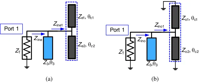
The proposed circuit structure of the band-stop filter is shown in Figure 1. Two parallel-coupled lines of different electrical lengths, and two open-circuit stubs are added in shunt symmetrically. The characteristic impedances of the two coupled lines are denoted as Ze1, Zo1, Ze2, Zo2, and the characteristic impedance of the open-circuit stub is Z3. For convenience, both the upper and lower coupled line structures are assumed to have the same even- and odd-mode electrical length (θc1=θe1 =θo1,θc2 =θe2=θo2), and the corresponding electrical lengths of the open-circuit stubs are both θ3. ZT is the port impedance. According to the symmetrical network analysis results [1, 9], the network analysis of Figure 1 will be simplified by analyzing the one-port networks shown in Figure 2. Based on the analysis theory [1, 5], the input impedances Zine and Zino shown in Figure 2 can be expressed by
Zine =
Zine1×j Z3 tanθ3
Zine1+j Z3 tanθ3
, (1a)
Zino =
Zino1×j Z3 tanθ3
Zino1+j Z3 tanθ3
, (1b)
in which
Zine1 = Ze1 jtanθc1
× Ze2 jtanθc2 Ze1
jtanθc1
+ Ze2
jtanθc2
, (2a)
Zino1 = jZo1
tanθc1×jZo2tanθc2 jZo1tanθc1+jZo2tanθc2.
(2b)
Port 1 Port 2
ZT ZT
Ze2,Zo2,θc2
Ze1,Zo1,θc1
Z3,θ3 Z3,θ3
Port 1
ZT
Z3,θ3
Ze1, θc1
Ze2, θc2
Zine1
Zine
Port 1
ZT
Z3,θ3
Zino1
Zino
Zo1, θc1
Zo 2, θc2
(a) (b)
Figure 2. The equivalent simplified circuit structures of the band-stop filter under (a) even-mode and (b) odd-mode excitations.
Therefore, the even- and odd-mode input impedancesZine andZino can be expressed as
Zine = −j Ze1Ze2Z3
Ze1Ze2tanθ3+Z3(Ze1tanθc2+Ze2tanθc1),
(3a)
Zino = j Zo1Zo2Z3tanθc1tanθc2
Z3(Zo1tanθc1+Zo2tanθc2)−Zo1Zo2tanθc1tanθc2tanθ3. (3b) Then, the even- and odd-mode scattering parameters of this proposed band-stop filter can be calculated by [1]
S11e = Zine−ZT
Zine+ZT, (4a)
S11o = Zino−ZT
Zino+ZT. (4b)
When the symmetrical property is considered, the external scattering parameters can be expressed by [1]
S11 = S22= S11e+S11o
2 , (5)
S21 = S12= S11e−S11o
2 . (6)
By combining (4)–(6), the mathematical expressions of scattering parameters are
S11 = ZineZino−Z
2 T
(Zine+ZT)(Zino+ZT), (7)
S21 = (Zine−Zino)ZT
(Zine+ZT)(Zino+ZT). (8)
The condition of transmission poles (reflection zeros) can be obtained when
|S11|= 0, (9)
and transmission zeros can be obtained when
|S21|= 0. (10)
Hence, the final Equations (9) and (10) including the characteristic impedances and electrical lengths are
Ze1Ze2Zo1Zo2Z32tanθc1tanθc2 [Ze1Ze2tanθ3+Z3(Ze1tanθc2+Ze2tanθc1)]
×[Z3(Zo1tanθc1+Zo2tanθc2)−Zo1Zo2tanθc1tanθc2tanθ3]
and
Ze1×Ze2 Ze1tanθc2+Ze2tanθc1
=j Zo1Zo2tanθc1tanθc2 Zo1tanθc1+Zo2tanθc2.
(12)
According to the analytical Equations (1)–(12), the external scattering parameters performance (including magnitude and phase information) of this novel band-stop filter can be calculated and analyzed. The band-stop filter’s center frequency is normalized at 1 GHz, and it leads to transmission zeros distributed by pairs symmetrically placed around the center frequency. If the line lengths are chosen appropriately, the band-stop performance at the operating frequency will be determined.
3. ANALYSIS OF CIRCUIT ELECTRICAL PARAMETERS
To illustrate the performance of the filter, which is affected by characteristic impedances of the coupled lines (Ze1,Zo1,Ze2,Zo2) and the open-circuit stubs (Z3), five parts of discussion will be represented according to the proposed analytical approach above. For simplicity, the electrical lengths have been decided asθc1= 34π,θc2 = π4,θ3 = π2, and all values of the port impedanceZT of the following examples are equal to50 Ω.
3.1. The influence of Ze2 and Zo2 on the Transmission Zeros and Reflection Zeros of the Proposed Filter
It can be observed from the Equations (11) and (12) that the transmission zero of the filter is determined byZe1,Zo1,Ze2,Zo2 as well asθc1 andθc2. In the case thatθc1andθc2are predetermined, the values of Ze1,Zo1,Ze2,Zo2 are important factors leading to various transmission zeros and reflection zeros. The analysis of Ze2 and Zo2 is taken for example. The frequency points of transmission zeros and reflection zeros with different Ze2 and Zo2 are plotted in Figure 3 and Figure 4 respectively. The rest of the design parameters are uniformly determined asZe1 = 140 Ω,Zo1= 105 Ω, Z3= 122 Ω. It can be clearly observed in Figure 3 and Figure 4 that the number of transmission zeros is affected by Ze2 and Zo2. In Figure 3, Zo2 is fixed as 120 Ω. When Ze2 < 115 Ω, the filter has three transmission zeros in the stopband. The number of zeros decreases to two when 115 Ω < Ze2 <123 Ω. And when Ze2 >123 Ω, there is just one zero in the stopband. In Figure 4,Ze2 is fixed as 140 Ω. Similarly, the filter has three transmission zeros when Zo2 <103 Ω, two zeros when 103 Ω< Zo2<109 Ω and one whenZo2>109 Ω. Besides, Figure 3 shows that the upper reflection zero becomes closer to the transmission zero whenZe2 increases while the lower has no obvious change. The lower reflection zero increases whenZo2 increases while the upper invariants in Figure 4. In other words, the selectivity is optimized with the increase of
100 110 120 130 140 150 160 170 180 190 200
0.4 0.6 0.8 1.0 1.2 1.4 Fr e que nc y Poin ts (GHz ) Z
e2 (Ω)
Transmissi on zero Low er reflection zero Upper ref lection zero
90 100 110 120 130 140 150 0.4
0.6 0.8 1.0 1.2
Fr
e
que
nc
y
Poin
ts
(GHz
)
Zo2 ( )
Transmissi on zero Low er reflection zero Upper reflection zero
Ω
Figure 4. Frequencies of transmission zeros and reflection zeros with differentZo2.
Ze2 and Zo2. Figure 3 and Figure 4 can be considered as a useful guidance of the selection of Ze2 and Zo2.
3.2. The Influence of Ze1 on the Performance of the Proposed Filter
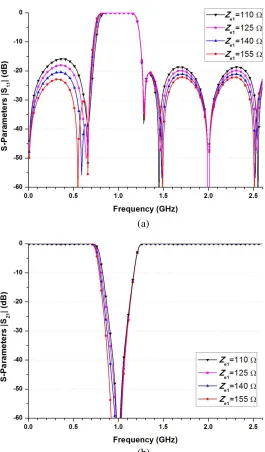
When other electrical parameters are fixed, the variation ofZo1 andZe1 will affect the characteristics of the filter. For convenience, only the value ofZe1 has been changed. The electrical parameters’ values of the filter are given in Table 1. Based on these values, the ideal scattering parameters can be calculated using Equations (1)–(12), and their magnitude responses are plotted in Figures 5(a) and (b) respectively. From Figure 5(a), it can be seen that the return loss in passband changes regularly with the variation ofZe1: Example A4 has the highest passband return loss (larger than 23 dB) while Example A1 has the lowest one (smaller than 17 dB). Furthermore, the first reflection zero decreases with Ze1 increasing. And the number of reflection zeros is six in Example A1 while the number of the other three examples is seven. Therefore different numbers of reflection zeros can be obtained by choosing Ze1 properly. Besides, the selectivity is improved whenZe1 increases, as illustrated in Figure 5(b).
Table 1. The electrical parameters’ values for the band-stop filter with variableZe1.
Parameters Example A1 Example A2 Example A3 Example A4
Ze1 (Ω) 110 125 140 155
Zo1 (Ω) 105 105 105 105
Ze2 (Ω) 140 140 140 140
Zo2 (Ω) 120 120 120 120
Z3 (Ω) 122 122 122 122
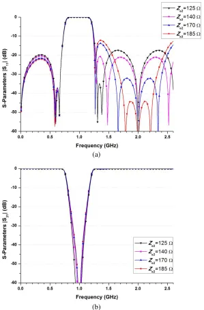
3.3. The Influence of Ze2 on the Performance of the Proposed Filter
(a)
(b)
Figure 5. The scattering parameters (a) |S11| and (b) |S21| of the bandstop filter when Ze1 = 110, 125, 140 and 155 Ω.
Table 2. The electrical parameters’ values for the band-stop filter with variableZe2.
Parameters Example B1 Example B2 Example B3 Example B4
Ze1 (Ω) 140 140 140 140
Zo1 (Ω) 105 105 105 105
Ze2 (Ω) 125 140 170 185
Zo2 (Ω) 120 120 120 120
(b) (a)
Figure 6. The scattering parameters (a) |S11| and (b) |S21| of the filter when Ze2 = 125, 140, 170, 185 Ω.
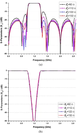
Table 3. The electrical parameters’ values for the band-stop filter with variableZ3.
Parameters Example C1 Example C2 Example C3 Example C4
Ze1 (Ω) 140 140 140 140
Zo1 (Ω) 105 105 105 105
Ze2 (Ω) 140 140 140 140
Zo2 (Ω) 120 120 120 120
3.4. The Influence of Z3 on the Performance of the Proposed Filter
Table 3 shows the electrical parameters’ values. Only the value of Z3 is changed. The calculated scattering parameters of these four examples are illustrated in Figures 7(a) and (b). Obviously, the return loss performance in the passband of ExampleC4 is the best among four examples, which is larger than 20 dB as shown in Figure 7(a). However, note that the number of reflection zeros of Example C4is six while the number of the other three examples is seven. What’s more, the selectivity and operating bandwidth at 1 GHz changes slightly for all the Examples C1–C4, as illustrated in Figure 7(b).
(a)
(b)
According to the number of transmission zeros, two types of ideal filters operating at 1 GHz are designed based on the previous analysis, especially Equations (11) and (12):
Case 1: This filter has only one transmission zero in the stopband with the following electrical parameters: ZT = 50 Ω, Ze1 = 140 Ω, Zo1 = 105 Ω, Ze2 = 140 Ω, Zo2 = 120 Ω, Z3 = 122 Ω, θc1 = 34π, θc2 = π4, θ3 = π2. Based on the lossless transmission-line and coupled-line models, the calculated scattering parameters are shown in Figure 8. The 20-dB band-stop fractional bandwidth is about 29.44% (0.84 GHz–1.13 GHz) and the return loss in the passband is larger than 20 dB.
0.0 0.5 1.0 1.5 2.0 2.5
-60 -50 -40 -30 -20 -10 0
S
-Para
mete
rs (d
B
)
Frequency (GHz)
S11 S21
Figure 8. The calculated scattering parameters|S11|and|S21|of Case 1.
Case 2: Based on the analytical approach in Section 2 and Section 3, the filter with two transmission zeros in the stop-band can be obtained after tuning electrical parameters. Ze2 and Zo2 are modified as Ze2 = 135 Ω andZo2= 107 Ω. The calculated scattering parameters are shown in Figure 9. The 20-dB band-stop fractional bandwidth is about 30.91% (0.83 GHz–1.14 GHz). However, the return loss in the passband is smaller than 20 dB.
0.0 0.5 1.0 1.5 2.0 2.5
-100 -90 -80 -70 -60 -50 -40 -30 -20 -10 0
S-Par
amete
rs
(dB
)
Frequency (GHz)
S 11 S
21
4. SIMULATED AND MEASURED EXAMPLES
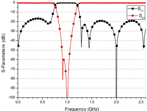
To verify the design method, a standard filter is fabricated on Rogers R04350B with a relative dielectric constant of 3.48 and dielectric thickness of 0.762 mm. Figure 10 shows the microstrip layout (a) and the practical photograph (b) of the band-stop filter separately. The dimensions of this filter are determined as follows: W s= 1.8 mm, W1 = 0.25 mm,W2= 0.2 mm, W3 = 0.25 mm,L1 = 70.8 mm, L2= 22.9 mm, L3 = 47.3 mm, LS = 7.5 mm, S1 = 0.85 mm, S2 = 1.4 mm, S3 = 1.3 mm. A full-wave simulator Sonnet Lite has been applied to obtain and efficiently tune the physical dimensions. Measurements are carried out using an Agilent N5230C network analyzer. The simulated and measured scattering parameters and group delay performance are shown in Figure 11 and Figure 12 separately. As shown in Figure 11, the full-wave simulated and measured scattering parameters are in good agreement. The measured operating stopband of the filter is centered at 0.94 GHz (ideal value is 1 GHz) with a 3-dB cutoff frequency bandwidth of 58.2%. The attenuation levels in the band from 0.71 to 1.16 GHz are larger than 10 dB. The measured maximum attenuation level is −46.88 dB at 1.05 GHz (very close to the ideal value 1 GHz). The measured out-of-band return loss in the range of 0 to 0.65 GHz is larger than 10 dB while the measured out-of-band return loss in the range of 1.3 to 2.6 GHz is larger than
(a)
(b)
Figure 10. (a) The microstrip layout and (b) photograph of the band-stop filter.
than 1.15 dB in the range of 1.3 to 2.6 GHz. As shown in Figure 12(a), the maximum measured group delay is 2.43 ns while the minimum is 0.16 ns in the low passband (range from 0 to 0.65 GHz). As for the upper passband group delay shown in Figure 12(b), the maximum is 2.50 ns, and the minimum is 0.51 ns in the range of 1.23 to 2.6 GHz. Finally, in order to clearly highlighting the advantages of this proposed filter, the performance comparison with other recently published similar filters is listed in Table 4.
0.0 0.1 0.2 0.3 0.4 0.5 0.6 0.7
0.0 0.5 1.0 1.5 2.0 2.5 3.0 Gr oup De la y (ns ) Frequency (GHz) (a)
1.2 1.4 1.6 1.8 2.0 2.2 2.4
0.0 0.5 1.0 1.5 2.0 2.5 3.0 Gr ou p D e la y ( n s ) Frequency (GHz) (b)
Figure 12. The measured group delay performance of (a) the low passband and (b) the upper passband of the band-stop filter.
Table 4. The comparison between the proposed and previous band-stop filters.
Coupled-line implementations Selectivity Size Bandwidth Layout Feasibility
Ref. [2] No Low Small Narrow High
Ref. [4] No High Large Wide Low
Ref. [8] Yes Low Large Dual-band Medium
Ref. [9] Yes Low Medium Wide High
This work Yes High Medium Wide High
5. CONCLUSION
ACKNOWLEDGMENT
This work was fully supported by “Training Programs of Innovation and Entrepreneurship for Undergraduates in BUPT (2014)” and in part by National Key Basic Research Program of China (973 Program) (No. 2014CB339900) and National Natural Science Foundation of China (No. 61201027).
REFERENCES
1. Hong, J.-S. and M. J. Lancaster, Micro-strip Filters for RF/Microwave Applications, Chapters 2 and 6, Wiley, New York, 2001.
2. Fallahzadeh, S. and M. Tayarani, “A compact microstrip bandstop filter,” Progress In Electromagnetics Research Letters, Vol. 11, 167–172, 2009.
3. Wang, J., H. Ning, Q. Xiong, M. Li, and L. Mao, “A novel miniaturized dual-band bandstop filter using dual-plane defected structures,” Progress In Electromagnetics Research, Vol. 134, 397–417, 2013.
4. Velidi, V. K., A. B. Guntupalli, and S. Sanyal, “Sharp-rejection ultra-wide bandstop filters,”IEEE Microwave and Wireless Components Letters, Vol. 19, No. 8, 503–505, 2009.
5. Wu, Y. and Y. Liu, “A coupled-line band-stop filter with three-section transmission-line stubs and wide upper pass-band performance,” Progress In Electromagnetics Research, Vol. 119, 407–421, 2011.
6. Wu, Y., Y. Liu, S. Li, and C. Yu, “A simple microstrip bandpass filter with analytical design theory and sharp skirt selectivity,”Journal of Electromagnetic Waves and Applications, Vol. 25, Nos. 8–9, 1253–1263, 2011.
7. Mrinal, K., K. Vamsi, S. Sanyal, and A. Bhattacharya, “Design of ultra-wideband band-stop filter with three transmission zeros,” Microwave and Optical Technology Letters, Vol. 50, No. 11, 2955– 2957, 2008.
8. Wang, W., M. Liao, Y. Wu, and Y. Liu, “Small-size high-selectivity bandstop filter with coupled-line stubs for dual-band applications,” Electronics Letters, Vol. 50, No. 4, 286–288, 2014.