SINRD Circuits Analysis with WCIP
Ahmad Ismail Alhzzoury1, 2, 3, *, Nathalie Raveu1, 2, Olivier Pigaglio1, 2, and Henri Baudrand1, 2
Abstract—This article presents the Wave Concept Iterative Procedure (WCIP), an efficient method for characterization of substrate integrated Non-Radiative Dielectric (SINRD) passive circuits based on wave concept formulation and its iterative solution. WCIP simulations are compared to measurements and Finite Element Method simulations. A good agreement is achieved with computation time saving.
1. INTRODUCTION
The development of millimeter and submillimeter devices has revolutionized the telecommunication systems, but their development is contained in terms of effort and time. Microwave structures require ease of integration, low loss and high performance.
The dielectric waveguides have received little attention in the past because of two fundamental problems: radiation losses due to discontinuities and difficulty to transcribe these circuits in planar technology. The NonRadiative Dielectric waveguide (NRD), is first proposed by Yoneyama and Nishida [1] in 1981. It consists in a strip of dielectric substrate inserted between two metallic planes. The new manufacturing Substrate Integrated Circuits (SICs), have been proposed for the realization of NRD waveguide. This new technique, called SINRD, allows the integration of NRD waveguide on substrates [2, 3]. The advantage of SINRD waveguide is its ability to be integrated on the same dielectric substrate as the SIW technology [4]. The SINRD waveguide uses a network of holes, which reduces the dielectric constant of the substrate in the regions of interest. These circuits may be analyzed by full-wave analysis software based on Finite-Difference Time-Domain (FDTD) [5], Method of Moments (MoM) [6] or Finite element method (FEM) [7] and recently with semi-analytical method based on Greens function [8]. All these methods need large memory storage as well as calculation time.
In this paper, the WCIP method is extended to study substrate integrated structures. The advantage of this method remains in its ease of use due to the absence of test functions; its fast computation time, mainly due to the systematic use of Fast Mode Transform (FMT), and a gridded mesh use. This method proved its efficiency through several studies of Substrate Integrated Waveguide (SIW) [9–11]. To validate the proposed approach, several examples of SINRD structure are considered. Scattering coefficients obtained with the WCIP are successfully compared to published results, measurements and simulations obtained from other methods.
In the first part of this paper, the WCIP theory is described. In the second part, examples of SINRD structure are considered SINRD waveguides and bandpass filters. Simulated results are compared to measurements and simulations obtained from other numerical techniques so as to validate the proposed method.
Received 26 May 2014, Accepted 4 August 2014, Scheduled 16 August 2014
* Corresponding author: Ahmad Ismail Alhzzoury ([email protected]).
2. THEORY
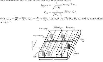
This method has been modified to study SIW [12] and proved to be efficient [11]. The circuit is described on a gridded mesh of regular cells. Vias are assumed in each cell but they can be differentiated by boundary conditions (empty, source, metallic, load or dielectric). The method assumes that holes are therefore drilled regularly along the two axes. An example is presented in Fig. 1.
Since the substrate is very thin, the electric scattered field in such structure is considered linearly polarized along z axis. In the present formulation, volumic waves, Az and Bz, are deduced from fields Ez and Jz in each cell through (1).
Az(i, j) = 2√1Z
0 (Ez(i, j) +Z0Jz(i, j)),
Bz(i, j) = 2√1Z
0 (Ez(i, j)−Z0Jz(i, j)).
(1)
Z0 is an arbitrary impedance; Ez is the electric field along z axis; Jz is the volumic current along z axis;i,j denote the cell position in the SIC grid. Fields are defined at the position of the via in each cell, through a projection on aH normalized function indicating the via position in the cell [12].
2.1. The Scattering Operator in Spatial Domain
On each via, Az is generated by Bz depending on boundary conditions on the via. All SIC structures can be constructed from five elementary cells that present different boundary conditions:
• for metallic cell: S(i, j) =−1; • for empty cell: S(i, j) = 1;
• for absorbing load cell: S(i, j) = 0;
• for source cell: S(i, j) = ZZosos+−ZZoo, (Zos: being the source internal impedance). • for cell with dielectric permittivity change:
S(i, j) = εg−j(εg−εr) εg+j(εg−εr),
where εr stands for the relative permittivity of the substrate and εg the relative permittivity of the dielectric via. These coefficients are resumed into (2):
Az = ˆSBz+A0 (2)
where ˆS takes into account the boundary conditions in the spatial domain. A0 is a source term to specify which via hole is excited initially.
2.2. The Scattering Operator in Modal Domain
The substrate height h is considered small enough to have only a surface TM mode within z ∈ [0, h], and the fields are assumed to be only oriented along the via. The relation between the waves in the spectral domain is given by:
˜
Bz = ˆΓ ˜Az, (3)
The modal scattering operator is defined by: ˆ
Γ =
pq|FpqΓpqFpq|, (4)
The modal scattering coefficient is:
Γpq= Zpq−Zo Zpq+Zo,
(5)
where, the modal impedance is defined according to [11]:
Zpq =
m,n
jωμ0|H|fpq,mn|2 k02εr−α2p,m−βq,n2
withμ0 the permeability of the substrate,ω the angular frequency,fpq,mn the modal basis function on the elementary cell of size (dx ×dy) bounded by periodic walls as detailed in (7), and Fp,q the modal basis function on the circuit of size (Dx×Dy) detailed on (8).
fpq,mn = 1
dxdy
ejαp,mxejβq,ny, (7)
Fpq = 1
DxDy
ej2Dxπpxej2Dyπqy, (8)
withαp,m = 2Dπpx +2dπmx ,βq,n = 2Dπqy +2dπny , (p, q, n, m) ∈Z4;Dx,Dy dx and dy dimensions are reported in Fig. 1.
Metallic via
Source
E0
Dielectric εg
Dx
dy
dx
Dy
Periodic walls
h
Dielectric εr
z x
y
0
load
Empty cell
Figure 1. Substrate integrated circuit example.
2.3. Iterative Process
The connection between the spatial domain and spectral domain is carried out via the Fast Modal Transform (FMT) and its inverse (FMT−1) (9).
˜
Az= FMT (Az) Bz= FMT−1
˜ Bz
, (9)
The iterative process defined in (10) is constructed via a multiple reflection procedure, which contains three main parts: source excitations, the spatial-domain and the spectral domain scattering.
Az = ˆSBz+A0 ˜
Bz= ˆΓ ˜Az ,
(10)
The system (10) [13, 14] is solved with GMRES [15]. Scattering parameters are then deduced.
Id−SˆFMT−1ΓFMTˆ
Az =A0, (11)
whereId is the identity matrix.
3. APPLICATION
In these applications, the number of vias is important, and therefore the hypothesis of homogeneity seems reasonable. As a consequence, we first derive the effective relative permittivity εeff with the
3.1. SINRD Waveguide
3.1.1. Characterization of the Effective Dielectric Permittivity
At first, we try to evaluate the homogeneous effective relative permittivity εeff of the drilled substrate.
This is achieved through two waveguide simulations (TE10 and TEM fundamental modes). Since homogeneity condition is assumed, the effective dielectric constant may be deduced from the cutoff frequency evaluation of the propagation constant.
3.1.1.1 TE10 Waveguide
The cutoff frequency of the TE10mode [16] is directly related to εeff (12). By changing the waveguide
widthDx, the cut-off frequency is changed andεeff is therefore deduced at each frequency.
fTE10
c =
c 2Dx√εeff
(12)
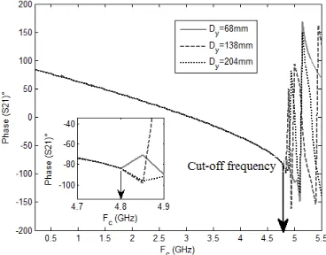
To obtain this cutoff frequency for a given waveguide width, the phase separation ofS21for different distancesDy between the two ports is simulated as presented in Fig. 2 with a frequency step of 0.5 GHz. Then the propagation constant is deduced and the cutoff frequency also as shown in Fig. 3. Here, the effective permittivity εeff is 2.0177 at 4.8 GHz for a width of 22 mm.
∠S21=−βDy
εeff =
β k0
2 =
∠S21 Dyk0
2 (13)
3.1.1.2 TEM Waveguide
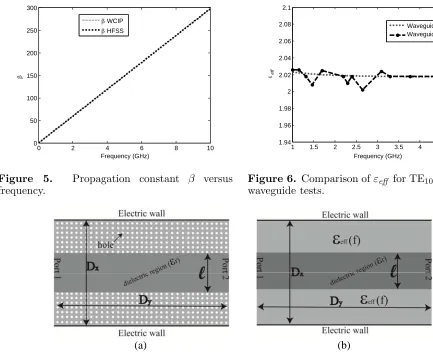
To determine εeff, the waveguide shown in Fig. 4 is addressed. By the same procedure, the effective
constant is obtained in this waveguide. For example, the propagation constant β deduced from WCIP and HFSS are compared (Dy = 68 mm) in Fig. 5. The maximum relative difference between the two
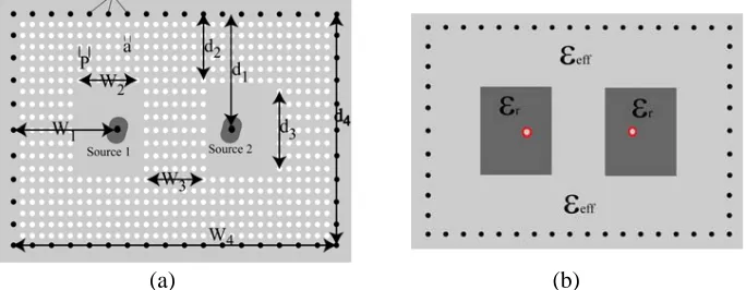
Figure 2. SINRD waveguide of fundamental mode TE10.
Figure 3. Phase of S21 for several distances by between ports.
p
Dy
Source 2
Periodic wall
Periodic wall
Magnetic walls
d d
a εg
εr
Magnetic walls
Source 1
0 2 4 6 8 10 0
50 100 150 200 250 300
Frequency (GHz)
β
β WCIP
β HFSS
Figure 5. Propagation constant β versus frequency.
1 1.5 2 2.5 3 3.5 4 4.5 5
1.94 1.96 1.98 2 2.02 2.04 2.06 2.08 2.1
Frequency (GHz)
εeff
Waveguide TEM Waveguide TE10
Figure 6. Comparison of εeff for TE10and TEM waveguide tests.
(a) (b)
Figure 7. Dielectric waveguide structures for (a) WCIP, (b) equivalent waveguide for HFSS.
methods is of 0.7% (with respect to WCIP). The simulation time with the WCIP is 0.32 s against 1.1 s for the HFSS for one frequency point simulation (CPU: Intel Core 2 Due E6550 @ 2.33 GHz, RAM: 4 Go).
In Fig. 6, the two methods used forεeff evaluation are compared; they are both in good agreement.
With TEM mode evaluation the εeff(f) is obtained with one simulation and is not dependant on the
waveguide size step, therefore this method is more convenient and will be preferred for future study.
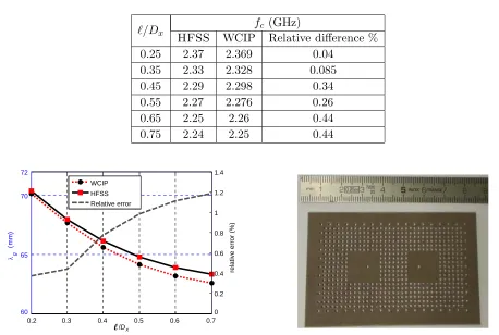
3.1.2. Characterization of SINRD Waveguide
Here, the properties of the SINRD waveguide shown in Fig. 7(a) are determined. The width of the dielectric strip is being changed while the total width of the waveguide is kept constant Dx = 40 mm. Thus, the cut-off frequency of the SINRD waveguide fc is changing as well. The equivalent waveguide, shown in Fig. 7(b), is simulated by HFSS with the εeff determined in the previous paragraph.
We note (Table 1) that the cutoff frequency obtained by the complete calculation (WCIP) corresponds to the simplified calculation using the condition of homogenization (εeff of Fig. 6 with
TEM fundamental mode tests) regardless of/Dx. The relative difference between the values obtained by WCIP and HFSS is 0.45%.
Table 1. Cut-off frequency of the SINRD waveguide of Fig. 7.
/Dx fc
(GHz)
HFSS WCIP Relative difference %
0.25 2.37 2.369 0.04
0.35 2.33 2.328 0.085
0.45 2.29 2.298 0.34
0.55 2.27 2.276 0.26
0.65 2.25 2.26 0.44
0.75 2.24 2.25 0.44
0.2 0.3 0.4 0.5 0.6 0.7
60 65 70 72
λg
(
mm)
0 0.2 0.4 0.6 0.8 1 1.2 1.4
relative error (%)
WCIP HFSS Relative error
/Dx
Figure 8. Guided wavelength λg depending on /Dx.
Figure 9. Photograph of the drilled substrate of the SINRD filter (order 2).
frequencies above the cut-off frequency of the waveguide using (14) and (15):
∠S21 = −βDy = − 2πDy
λg
(14)
λg = − 2πDy
∠S21
= −360∗Dy
∠S21◦
(15)
The wavelength of the waveguide deduced from (15) is evaluated by HFSS and the WCIP. In Fig. 8, there is a good agreement between the results obtained by the WCIP and those from HFSS, when the condition of homogeneity is verified (the full calculation with holes can not be done using HFSS). The relative difference does not exceed 1.2%. The simulation time with the WCIP, for /Dx = 0.25, is of 0.34 s against 1.36 s for the FEM software for one frequency point simulation. The greater the ratio /Dx, the lower the ratio of the holes in the waveguide, hence the more we move away from the condition of homogenization and the more is the difference between the wavelength obtained with WCIP and that obtained with HFSS.
3.2. SINRD Filter
3.2.1. Fabrication
To achieve these prototypes of SINRD filter, copper surfaces of the substrate are removed. Every hole has to be drilled in the substrate. Ground planes were made with brass plates reported on each side of the drilled substrate. To achieve the metallic vias, the substrate was first drilled, then drilling the two brass plates and then connecting together with the metallic vias of diameter 1.25 mm.
For coaxial connectors, two holes of the same diameter were drilled in the dielectric plate and the lower brass, to connect the central conductor of the SMA connector. In the top brass plate, there is a hole of 4.2 mm diameter to not short-circuit the connector; 4.2 mm diameter corresponds to the inner diameter of the Teflon in the SMA connector. One achieved drilled substrate is shown in Fig. 9.
3.2.2. Design of SINRD Filter of 2nd Order
The drilled substrate has been replaced by a homogeneous substrate of relative effective dielectric permittivity εeff obtained in 3.1.1 for memory cost reasons in HFSS simulation, as mentioned in the
previous section. In this analysis, εeff is frequency dependant.
The bandpass filter specifications are: a center frequency of 3.8 GHz, a relative bandwidth of 17%, a ripple of 0.05 and an order 2. The resulting filter presents two resonators and one inverter and is represented in Fig. 10(a). Its equivalent filter for HFSS simulation is presented in Fig. 10(b). Dimensions of the SINRD filter are detailed in (Table 2).
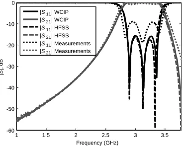
The reflection coefficientS11and the transmission coefficientS21are plotted in Fig. 11. Simulations of the filter with HFSS and WCIP and measurements are in good agreement. The simulation time with the WCIP is of 4.3 s against 6.22 s for the FEM software for one frequency point simulation (CPU: Intel Core 2 Due E6550 @ 2.33 GHz, RAM: 4 Go). It should be noted that even though the WCIP takes the holes in consideration during the simulation, it is still faster than the simplified calculation using the HFSS.
3.2.3. Design of SINRD Filter of 3rd Order
The substrate is the same as in the previous part. The bandpass filter specifications are: a center frequency of 3.13 GHz, relative bandwidth of 23%, a ripple of 0.012 and an order 3. The resulting filter
(a) (b)
Figure 10. (a) SINRD filter of 2nd order, (b) equivalent homogeneous filter for HFSS simulation.
Table 2. Dimensions of the SINRD filter of second order.
Symbol Value (mm) Symbol Value (mm)
w1 22 d3 10
w2 12 d4 40
w3 14 p 2
w4 68 a 1.25
d1 20 h 1.524
d2 14
Table 3. Dimensions of the SINRD filter of third order.
Symbol Value (mm) Symbol Value (mm)
w 148 d1 14
w1 30 d2 20
w2 40 d3 10
w3 14 p 2
w4 20 a 1.25
1 2 3 4 5 Frequency (GHz)
|S11| WCIP
|S21| WCIP
|S21| HFSS
|S11| HFSS
|S21| Measurements
|S11| Measurements
-30 -25 -20 -15 -10 -5 0
|S
|, dB
Figure 11. S-parameters of the filter of Fig. 10.
(a) (b)
Figure 12. (a) SINRD filter of 3rd order, (b) equivalent homogeneous filter for HFSS simulation.
1 1.5 2 2.5 3 3.5
-60 -50 -40 -30 -20 -10 0
Frequency (GHz)
|S
|, dB
|S | WCIP |S | WCIP |S | HFSS |S | HFSS |S | Measurements |S | Measurements
11
21
11
21
11
21
Figure 13. S-parameters of the filter of Fig. 12.
presents three resonators and two inverters and is represented in Fig. 12(a). Its equivalent filter for HFSS simulation is presented in Fig. 12(b). Dimensions of the SINRD filter are detailed in (Table 3).
S-parameters response of this filter is shown in Fig. 13. The simulations with HFSS and WCIP and measurements are in good agreement. The simulation time with the WCIP is of 7.3 s against 12 s for the FEM software for one frequency point simulation. It should be noted that even though the WCIP takes the holes in consideration during the simulation, it is still faster than the simplified calculation using the HFSS.
4. CONCLUSION
REFERENCES
1. Nishida, S. and T. Yoneyama, “Nonradiative dielectric waveguide for millimeter-wave integrated circuits,” IEEE Transactions on Microwave Theory and Techniques, Vol. 26, No. 11, 1188–1192, Nov. 1981.
2. Wu, Y. and K. Cassivi, “Substrate integrated NRD (SINRD) guide in high dielectric constant substrate for millimeter wave circuits and system,” IEEE MTT-S International Microwave Symposium Digest, Vol. 3, 1639–1642, Jun. 2004.
3. Cassivi, Y. and K. Wu, “Substrate integrated nonradiative dielectric waveguide,” IEEE Microwave and Wireless Components Letters, Vol. 14, No. 3, 89–91, Mar. 2004.
4. Wu, K. and F. Boone, “Guided-wave properties of synthesized nonradiative dielectric waveguide for substrate integrated circuits (SICs),” IEEE MTT-S International Microwave Symposium Digest, Vol. 2, 723–726, 2001.
5. Simpson, J. J., A. Taflove, J. A. Mix, and H. Heck, “Computational and experimental study of a microwave electromagnetic bandgap structure with wave guiding defect for potential use as a bandpass wireless interconnect,” IEEE Microwave and Wireless Components Letters, Vol. 14, 343– 345, 2004.
6. Yang, H.-Y. D. and D. R. Jackson, “Design consideration for modeless integrated circuit substrates using planar periodic patches,”IEEE Transactions on Microwave Theory and Techniques, Vol. 48, No. 12, 2233–2239, 2000.
7. Zhou, L. and L. E. Davis, “Finite element method with edge elements for waveguides loaded with ferrite magnetized in arbitrary direction,” IEEE Transactions on Microwave Theory and Techniques, Vol. 44, No. 6, 809–815, Jun. 1996.
8. Arnieri, E. and G. Amendola, “Analysis of substrate integrated waveguide structures based on the parallel-plate waveguide Green’s function,” IEEE Transactions on Microwave Theory and Techniques, Vol. 56, No. 7, 1615–1623, 2008.
9. Zairi, H., H. Baudrand, A. Gharsallah, and A. Hafidh Gharbi, “An efficient iterative method for analysis of a substrate integrated waveguide structures,”Microwave and Optical Technology Letters, Vol. 52, No. 1, 45–48, 2010.
10. Ismail Alhzzoury, A., N. Raveu, G. Prigent, O. Pigaglio, H. Baudrand, and K. Al-Abdullah, “Substrate integrated waveguide filter design with wave concept iterative procedure,” Microwave and Optical Technology Letters, Vol. 53, No. 12, 2939–2942, Dec. 2011.
11. Ismail Alhzzoury, A., N. Raveu, O. Pigaglio, H. Baudrand, and K. Al-Abdullah, “WCIP applied to substrate integrated waveguide,”Progress In Electromagnetics Research C, Vol. 33, 171–184, 2012. 12. Raveu, N. and H. Baudrand, “Metallic EBG characterization with the WCIP,” IEEE Antennas
and Propagation Symposium, APS-URSI, 1–4, Charlestown, 2009.
13. Girard, C., A. Zugari, and N. Raveu, “2D FDTLM hybridization with modal method,” Progress In Electromagnetics Research B, Vol. 55, 23–44, 2013.
14. Raveu, N., J. Vincent, J.-R. Poirier, R. Perrussel, and L. Giraud, “Physically-based preconditioner for the WCIP,”2012 Asia-Pacific Microwave Conference Proceedings (APMC), 1310–1312, Dec. 4– 7, 2012.
15. Saad, Y. and M.-H. Schultz, “GMRES: A generalized minimal residual algorithm for solving non symmetric linear systems,” SIAM J. Sci. and Stat. Comput., Vol. 7, No. 3, 856–869, Jul. 1986. 16. Pozar, D. M., Microwave Engineering, 4th Edition, John Wiley & Sons Ltd., 2011, ISBN: