Analysis of Three Phase T-Source Inverter
with Space Vector PWM Technique
G.Hemaprabha1, T.Rama Rajeswari2
Assistant Professor, Dept. of EEE, Info Institute of Engineering, coimbatore, Tamilnadu, India1
PG Student [PED], Dept. of EEE, Info Institute of Engineering, Coimbatore, Tamilnadu, India2
ABSTRACT: This paper deals with analysis of three phases source Inverter with space vector PWM technique. T-source impedance network is developed to overcome the drawbacks of Z-T-source inverter. The basic topology is known in the literature as a Z-source inverter (ZSI).It has flat reactive components in comparing with conventional ZSI. The T source Network can perform DC to AC power conversion and it provides buck boost operation in a single stage. Space vector pulse width modulation technique is used to produce the output voltage with less harmonics. T-Source inverter implemented with a space vector PWM technique for reducing the harmonics are simulated using MATLAB Simulink.
KEYWORDS: Z-source inverter, T-Source inverter, Space vector pulse width modulation,Total Harmonic Distortion (THD)
I.INTRODUCTION
The inverter is a device which converts direct current to alternating current. It can divide into two traditionally inverters: voltage-source inverter and current-source inverter. In VSI, the output voltage cannot exceed the DC source voltage. So the DC – DC boost converter is utilized when the DC source is limited. The input to the inverter bridge is a constant voltage source.The constant voltage source is found by connecting a large capacitor across the DC source. Dead time is necessary to prevent the short circuit of upper and lower switching devices in each phase leg. In CSI, the output voltage cannot be lower than the DC source. The input to the inverter bridge is a constant current source.A large inductor with the DC source connected in series provide a constant current source.Overlap time between phase legs is necessary to avoid the open circuit of upper or lower switching devices.These drawbacks are overcome in Z- source Inverter.TSI requires a very low leakage inductance transformer with high precision.It makes use of shoot through in the inverter bridge to boost the voltage in the VSI or to buck the voltage in the CSI.The Z-source inverter is a buck– boost inverter. It has more passive components. To overcome this problem in T-source inverter is proposed.
In SVPWM methods, revolving reference vector is used to provide a reference voltage. In the line side, the magnitude and frequency of the fundamental component are controlled by the reference voltage vector magnitude and frequency, respectively. Space vector modulation developsa DC bus voltage and generate less harmonic distortion in a three phase voltage source inverter.
II.T-SOURCE INVERTER
Fig. 1Circuit Diagram for T-Source Inverter PRINCIPLE OF OPERATION:
There are two operating mode presents in T-source inverter. One mode is active and the other one is a Shoot-through mode. The T-network can be replaced with the LC-network for boosting the output voltage by inserting shoot through states in the PWM.
(i) Shoot through mode:
During the shoot through state output voltage boosting is involved. During this mode, the inductor is to limit the current ripple.During the shoot through inductor current increases linearly and the voltage across the inductor is same as the voltage across the capacitor. There is no voltage present across the load. Shoot through states are inserted within the zero state without affecting the active states.
Fig. 2 Equivalent Circuit of shoot through state (ii) Non shoot through mode:
(iii) Mathematical modelling:
By usin g Kir chh off’s laws an d voltage aver agin g can be devel op ed by TSI g over n in g equation s.For th e switch in g time per iod T, th e aver age voltage thr ough th e tr an sfor mer in ductan ces sh ould be equal to zer o.
1 0. c 1
.(
in c) /
0
V
T V
T V
V
n T
(1)
Both output voltage Vo u tan d capacitor voltage Vc are fun ction s of th e sh oot-th r ough coeffi cien t
D=(T
0/T)
(2)
1
/
1 1 .
C in T D V V n D
(3)
Where D satisfies a condition D<1/ (n+1). Therefore, the maximum value of D for TSI n>1is smaller than the Z-source. The same output voltage can be obtained by achieving a smaller time period of short circuits transistor current from the TSI in n>1in comparison with ZSI. Using the amplitude of voltage Vdc in non-shoot-through states can find from:
/ 1 (
1).
dc in
V
V
n
D
(4)
Actually, th e in fluen ce of leakage on in ductan ce in th e tran sfor mer is ver y impor tan t. In T sour ce in ver ter, th e leakage in ductan ce is ver y less because both th e primar y win din g an d secon dar y win din g ar e placed in a sin gle ir on cor e. Th e perfor man ce of TSI depen ds on th e accur acy of th e tran sfor mer design.
Th e peak dc lin k voltage acr oss th e in ver ter is expressed as,
0 1 d c T V T T
(5) Wh er e,
0 1 1 T B T T (6)
B is th e Boost fact or r esultin g in th e sh oot thr ough state T0 is th e sh oot thr ough time period in sec
T1 is th e n on -sh oot thr ough time per iod in sec
Th e in ver ter can be expr essed by th e output peak ph ase voltage ,
.
/ 2
dc dc
V
M V
(7)
Where M is the modulation index.
Usin g th e above equation s th e output peak voltage can be expr essed as,
. .
/ 2
ac dc
V
M B V
(8)
Thus th e output voltage can be stepped up an d down by ch oosin g an suitable Bu ck -Boost fact or BB.
B X
B
M
B
(9)
IV. PWM TECHNIQUES
The power electronics and drive systems are popular inSwitching techniques of pulse width modulation (PWM). PWM is most commonly used in applications like motor speed control, converters audio amplifiers, etc.. The main aim of the PWM is to control the inverter output voltage and reduce the harmonic content in the output voltage. The pulse width modulation (PWM) techniques are mainly used for voltage control. These techniques are more efficient and they control the drive of the switching devices. The different PWM techniques are used in T-source inverter.In this paper, Space Vector pulse width modulation technique is used.Space Vector PWM techniqueis used to control the output voltage as well as reduce the harmonics.
SPACE VECTOR PULSE WIDTH MODULATION
Principle of Space vector pulse width modulation
Six non-zero vectors are (V1,V2,V3,V4,V5,V6)sharp the axes of a hexagon and supplies power to the load. The angle
between anytwo adjacent non-zero vectoris 60 degrees.The two zero vectors(V
0 and V7) and are at the origin and apply
zero voltage to the load. The eight vectors are denoted by (V
0, V1, V2, V3, V4, V5, V6, V7) are called the basic space
vectors. The same transformation can be applied to the desired output voltage to get the desired reference voltage vector,V
ref in the d-q plane. By using the eight switching patterns,SVPWM technique is to estimate the reference
voltage vector V
ref.One simple method of approximation is generatedif the small period T is equal to Vref in the same
period such that the average output of the inverter is obtained.
Fig. 4 Basic switching, vectors and sectors.
SWITCHING STATES
Table.1Switching patterns and output vectors.
Realization of Space Vector PWM
Space vector PWM can be implemented by the following steps:
Step-1: Determine Vd, Vq, Vref, and angle (α).
Step-2: Determine the time duration, T1, T2 , and T0.
Step-3: Determine the switching time of each transistor (S1 to S6)
Step-1: Determine Vd, Vq, Vref, and angle (α) Vd, Vq, Vref and angle (α) can be found as follows:
1
1
.
.
2
2
d an bn cn
V
V
V
V
(10)
0 0
3 3
. cos 30 . cos 30
2 2
an
q
V V
(11)
1 1 1
2 2 2
.
3 3 3
0 2 2 a n d b n q c n V V V V V (12) 2 2
|
V
ref|
V
dV
q
(13)
1
t a n 2
d q V V
w t f t
Where f = fundamental frequency
Voltage vectors
Switching vectors
Line to neutral Voltage
Line to Line voltage
A B C Van Vbn Vcn Vab Vbc V0
V0 0 0 0 0 0 0 0 0 0
V1 1 0 0 2/3 -1/3 -1/3 1 0 -1
V2 1 1 0 1/3 1/3 -2/3 0 1 -1
V3 0 1 0 -1/3 2/3 -1/3 -1 1 0
V4 0 1 1 -2/3 1/3 1/3 -1 0 1
V5 0 0 1 -1/3 1/3 2/3 0 -1 1
V6 1 0 1 1/3 -2/3 1/3 1 -1 0
a
Fig. 5 Voltage space vector and its component in (d,q)
Step-2: Determine the time duration, T1, T2 , and T0
The switching time duration can be determined as follows:
Switching time duration at Sector 1
1 1 1 2
1 1 2
1 2 0
0 0
z
ref
T T T T T
T T T
V
V dt
V dt
V
(14)1 1 2
1 1 2
1 2 0
0 0
Z Z
T T T T T
ref
T T T
V
V dt
V dt
V
(15) 1 2 cos( )cos( ) 2 1 2 3
. | | . . . .
sin( ) 3 0 3
sin( ) 3
Z ref dc dc
T V T V T V
(16) 1
s i n 3 . .
s i n 3
Z
T T a
(17) 2
s i n . .
s i n 3 z
T T a
(18)
Switching time duration at any sector
0
3
. | | . s i n 3
Z r e f d c
n
T T V
V
(19)
(20)
T
0
T
Z
T
1
T
2(21)
Where,n=1 through 6 (that is sector 1 to 6),
0
60
r e f
V
1 2 Z
T T
V
1 1 Z
T
T
V
V
12
V
Fig. 6 Reference vector as a combination of adjacent vectors at sector-1.
Step 3: Determine the switching time of each transistor (S1 to S6)
V.SIMULATION RESULTS
Table 2 shows the system parameters used for simulation. The performance of the T-source inverter was tested under
space vector modulation technique.Fig 7, represents the simulation model for the generation of PWM pulses for TSI
by using SVPWM technique.
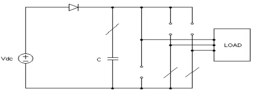
Sector
Upper (S1,S3,S5)
Lower (S4,S6,S2)
1 S1= T1 + T2+T0/2
S3= T2 + T0/2 S5 = T0/2 -T
S4=T0/2
S6=T1 + T0/2 + T S2 = T1 + T2 + T0/2 + 2T
2 S1= T1 +T0/2
S3= T1 + T2 + T0/2 S5 = T0/2 -T
S4=T2 + T0/2 + T S6=T0/2
S2 = T1 + T2 + T0/2 + 2T
3 S1= T0/2 - T
S3= T1 + T2 + T0/2 + T S5 = T2 +T0/2
S4=T1 + T2 + T0/2 +2T S6=T0/2
S2 = T1+ T0/2 + T
4 S1=T0/2 - T
S3= T1 + T0/2
S5 = T1 + T2 + T0/2 +T
S4=T1 + T2 +T0/2 + 2T S6=T2+ T0/2 + T S2 = T0/2
5 S1= T2+T0/2
S3= T0/2 - T
S5 = T1 + T2 +T0/2 +T
S4=T1 + T0/2 + T S6=T1 + T2 +T0/2 + 2T S2 =T0/2
6 S1= T1 + T2+T0/2 + T
S3= T0/2 - T S5 = T1 + T0/2
S4=T0/2
Table- 2. Parameters used for simulation
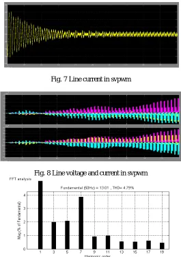
The Line current is shown in fig. 7.The Line voltage and current is shown in fig. 8. Harmonic spectrum of the output current is shown in fig. 9.
Fig. 7 Line current in svpwm
Fig. 8 Line voltage and current in svpwm
S.NO Parameters Values of simulation
1 DC supply voltage (Vdc) 200V
2 Capacitance (C) 218 × 10-3 F
3 Inductance (L) 20 × 10-6 H
4 Switching frequency 50 HZ
5 Snubber Resistance (Rs) 1 × 10⁵Ω
6 Diode Resistance (Rd) 0.01Ω
VI.CONCLUSION
This research deals with the Analysis of source inverter with Space vector pulse width modulation technique.The T-source impedance network provide the output voltage larger than the input voltage by proper maintaining the duty ratio of shoot-through state, voltage-source inverter and current-source inverter can’t be provide these advantages..All Pulse Width Modulation methods can be used to control T-source inverter. The THD obtained for 4.79% for SVPWM. In this paper using space vector PWM technique for boosting the voltage and reducing low harmonics in T-source inverter.
REFERENCES
[1] S.Thangaprakash, A. Krishnan “Implementation and Critical Investigation on Modulation Schemes of Three Phase Impedance Source Inverter”
Iranian Journal of Electrical & Electronic Engineering, 88 Vol. 6, No. 2, June 2010.
[2] Poh Chiang Loh, , D. Mahinda Vilathgamuwa, , Yue Sen Lai, Geok Tin Chua, and Yunwei Li, “ Pulse - Width Modulation of Z – source Inverters” IEEE Transactions on Power Electronics, Vol. 20, No. 6, November 2005.
[3] Sivaraman.P, A. Nirmalkumar, “ Modelling and Simulation of Photovoltaic Array fed T-Source Inverter” in International Conference onSustainable Energy and Intelligent System ,2011.
[4] Sivaraman.P, A. Nirmalkumar, “Analysis and Implementation of Novel TSI for High Voltage Gain Application” in International Review on Modelling and Simulations,2010.
[5] Sivaraman.P, A. Nirmalkumar, “Analysis of T-Source Inverter with Various PWM Schemes” in European Journal of Scientific Research,Vol.71 No.2 , pp. 203- 213,2012.
[6] F. Z. Peng: Z-Source Networks for Power Conversion, Proc. of 23rd Annual IEEE APEC’08, 2008, pp. 1258- 1265. [7] F.Z. Peng, “Z source inverter”, IEEE Trans. IndustryApplications,vol. 39, no. 2, pp. 504-510, March/April 2003.
[8] J. Rabkowski, R. Barlik, and M. Nowak, “Pulse WidthModulationmethods for bidirectional/high-performance Z-source inverter”, IEEEPower Electronics Specialists Conference, pp. 2750 –2756, June 2008.
[9] Marek Adamowicsz, Natalia Strzeleckal and Wieslaw Bury “New type T-source inverter” In proceeding on international conference of compatibility in power Electronics-2009 pp-191-195.
[10] Sivaraman P and Nirmalkumar A, “Analysis and implementation of a novel T-source inverter for high voltage gain application”International Review of Modeling and Simulation vol.5 pp 818-825 April 2012.
[11]K.Mahendran “Modified SVPWM For Modified ZSI” International Journal Dec 2011