Sparse Matrix Vector Multiplication
on a Field Programmable Gate Array
September 2007
Marcel van der Veen
University of Twente
Faculty of Electrical Engineering, Mathematics and Computer Science Computer Architecture for Embedded Systems (CAES) group
Committee:
Abstract
Abstract
Sparse Matrix Vector Multiplication (SMVM) has been a subject of research in the computer science field quite some time. The SMVM is an expensive operation used in the Conjugate Gradient algorithm. The Conjugate Gradient is an iterative algorithm used to solve linear equations.
The Finite Element Method is used in a lot of engineering areas like structural analysis, fluid dynamics, heat transport and electromagnetism. Within the Finite Element Method, the Conjugate Gradient algorithm is used to solve large sets of linear equations.
Within the research field of SMVM there are two directions, one direction tries to get the most out of general purpose processors while the other direction tries to make a fast implementation on a Field
Programmable Array. This project introduced a new method for the SMVM on a Field Programmable Gate Array called Small Bandwidth Coverage (SBC).
The main advantage of SBC is that the variation in performance caused by differences in the system matrices is only a factor two. Similar solutions have a variation in performance of a factor ten.
Preface
This project was carried out within the Computer Architecture for Embedded Systems (CAES) group. I would like to thank everybody of the CAES group for a great ambiance. Everyone was equal, professors, teachers, PhD-students and master students. I always suggest master students looking for a master thesis to take look at the CAES group because of the atmosphere.
I would like to mention a few people in particular.
Gerard Smit is professor and head of the CAES group. Despite his busy schedule he is always sincerely interested in the work of all the people working within the CEAS group. He is one of the main factors for providing a great atmosphere.
Pascal Wolkotte and Philip Hölzenspies are two PhD-students who are always interested in the work of others. Always asking good critical question and making suggestions to improve results.
Contents
Contents
1. Introduction ...1
2. Problem analysis...2
2.1. Finite Element Method ...2
2.1.1. Introduction ...2
2.1.2. System Matrix...3
2.1.3. Reordering ...4
2.1.4. Solvers ...4
2.2. Conjugate Gradient method...5
2.2.1. Introduction ...5
2.2.2. Steepest Descent ...7
2.2.3. Conjugate Gradient...9
2.2.4. Complexity analysis...10
2.3. Sparse Matrix-vector multiplication...11
2.3.1. Compressed Row Storage Format ...11
2.4. FEM Matrices...12
2.4.1. Example of a regular system matrix ...12
2.4.2. Example of a irregular system matrix...13
2.4.3. System matrix of the Volume Reconstruction algorithm...14
2.5. Field Programmable Gate Array...15
2.5.1. MAC unit...15
2.5.2. Processing Element...15
3. Design requirements ...17
4. Previous work...18
4.1. Striping based implementation ...18
4.2. Preprocessor implementation ...18
4.3. Straight forward implementation...18
4.4. Stripe method ...19
4.4.1. Stripes ...20
4.4.2. Construction of SRIO stripes...21
4.4.3. Systolic array ...22
4.4.4. Utilization ...23
4.4.5. Cause of low utilization ...26
4.4.6. Conclusion ...26
4.5. Parallel Matrix Communication Network ...27
4.5.1. Parallel Matrix Computation Network - Example ...28
4.5.2. SIO Example...29
4.5.3. Conclusion ...30
5. Alternative 1: Plans ...31
5.1. Computing the SMVM on one PE...31
5.1.1. Plans ...31
5.1.2. PE Design ...33
5.1.3. Mapping of the system matrix ...33
5.1.4. FPGA implementation ...36
5.1.5. Possible optimization...37
5.2. Computing the SMVM on Multiple PEs ...40
5.2.1. Introduction ...40
5.2.2. FPGA implementation ...44
5.2.3. Conclusion ...45
5.3. Preprocessing...46
5.3.1. Example...46
5.4. Conclusion...49
Contents
6.1. Short Review of Stripe Method ...50
6.1.1. Utilization of stripe method ...51
6.2. Small Band Coverage...51
6.3. Design of PE...53
6.4. PE band coverage ...53
6.5. SMVM with Small Band Coverage...54
6.5.1. Example...55
6.6. Problems...55
6.7. Partial Result Adder ...57
6.8. Preprocessing...59
6.8.1. Overhead...59
6.8.2. Division in matrix slices ...60
6.9. Controller ...62
6.10. Upper bound Utilization ...62
6.11. Preprocessor ...64
6.11.1. Dividing the bandwidth ...64
6.11.2. Scheduling the non-zero elements over the PEs ...67
6.12. Multi vector design...69
6.13. Total System...70
6.14. Conclusion...70
7. Results ...72
8. Future Work...74
8.1. Improving the partial result adder ...74
8.2. Symmetry ...74
8.2.1. Store partial results in local memory ...75
8.2.2. Convert CSC format into CSR format ...76
8.2.3. Conclusion ...77
8.3. Implementation...77
9. Conclusion...78
References 79
1. Introduction
1.
Introduction
The Finite Element Method (FEM) is a method often used for structural analysis to compute stress, deformations and internal forces on materials. It can also be used for fluid dynamics, heat transport, electromagnetism and other engineering areas. Recently this method is also used in a new research area: Volume Reconstruction in Diffuse Optical Tomography [1].
Car manufactures use the Finite Element Method for crash analysis. These analyses require a lot of computations. In [2] the execution time of different crash models for super computers is maintained. The crash analysis set is primarily used to compare the speed of different super computers with a real problem. One of the models is a crash with two cars (car2car model). The fastest time is set by the CRAY XT4 super computer with 512 AMD Dual Core Opteron processors running at 2.8 GHZ. Although this is a very fast system it still needs 6274 seconds (104 minutes) to complete [2]. A system with one Intel Dual Core Xeon processors running at 3.0 GHz needs 565261 seconds (157 hours) [2].
The speedup of the supercomputer scaled to 3.0 GHz is (565261/6274)*(3.0/2.8) = 96.5. Normally you would expect a speedup of 512.
The idea of Diffuse Optical Tomography is to reconstruct the 3D volume of tissue. This technique will be used at first instance for the diagnosis of breast cancer. The Volume Reconstruction algorithm in Diffuse Optical Tomography requires a lot of computations but needs to be completed in several minutes. At the moment, the target time is about fifteen minutes [1]. Besides the time to complete, other factors play a role such as costs and the size of the system. Because the amount of computations is substantial but not as much as the car2car model, a super computer would have enough processing power to fulfill the time
requirement. The disadvantage is that every system would need a super computer, which is expensive and uses a lot of energy.
2. Problem analysis
2.
Problem analysis
2.1. Finite
Element
Method
2.1.1. Introduction
As explained in the previous chapter the Finite Element Method (FEM) can be used to analyze all kinds of physical processes. The physical processes are represented with models. One of the examples often used to explain the Finite Element Method is the determination of stress and the bending of a truss bridge.
Figure 1
Figure 2
: Truss bridge
300 kN
The idea of FEM is to divide the mathematical model into a finite number of elements to construct a discrete model. For the discrete model of the truss bridge only one simple element has to be used. This simple element is the 2-node truss element (also known as bar). Figure 2 plots the discrete model of the truss bridge.
1
300 kN
2 3 4 5 6 7
12 11 10 9 8
: Discrete model of truss bridge
Each intersection of lines has become a node and every line is an element. The discrete model has 12 nodes (numbered from 1 to 12) and 21 elements. With some formulas it is easy to determine the individual reaction of the simple elements. By combining the individual reactions, the reaction of the complete truss bridge can be determined. The combined individual reactions result in a matrix, referred as system or stiffness matrix K. The size of the system matrix K depends on the number of nodes and the dimension used. The truss bridge is modeled in two dimensions with 12 nodes. This means that the size of the system matrix becomes 24 by 24, for each node there is an x and y component.
Within FEM the system that has to be solved is K u = f. The meaning of vector u and vector f depends on
the problem modeled. For mechanics the vector u represents the nodal displacement and vector f represents
2. Problem analysis
2.1.2. System Matrix
Consider the following one-dimensional problem.
1 5 3 2 4 20 kN
Figure 3
Figure 4
Figure 5
: one dimensional structure
The system to solve is K u = f.
: System to solve of the structure defined in figure 3.
The force on a node only depends on the displacement of de node itself and the displacement of its
neighbors. Thus the force on node one depends on the displacements of the node itself and the displacement of node five. The force on node two depends on the displacement of the node itself, node three and node four. Figure 3 represents the system matrix of the structure defined in figure 3. X indicates a non-zero value.
: System matrix K of structure defined in figure 3.
The system matrix K in general has some important properties. • The system matrix is sparse.
As seen in the example the force on a node only depends on its neighbors. The discrete models of real problems have usually more than 1,000 nodes while the number of neighbors lies in the order of ten. Meaning on average only 1% of the values are non-zero values. This results in a sparse matrix. • The system matrix is symmetric.
Consider figure 3. The distance and the material of the element between node one and node five determine the value of Kx1x5. This value is the relation between the displacement of node five and the
force on node one. Within the system matrix there is another value that represents the same element: Kx5x1. Thus for each element there are two values in the system matrix, one above and below the main
diagonal.
2. Problem analysis
2.1.3. Reordering
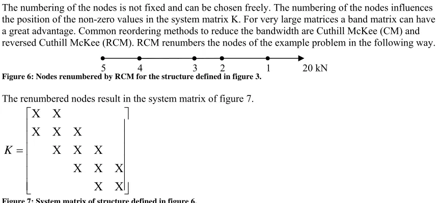
The numbering of the nodes is not fixed and can be chosen freely. The numbering of the nodes influences the position of the non-zero values in the system matrix K. For very large matrices a band matrix can have a great advantage. Common reordering methods to reduce the bandwidth are Cuthill McKee (CM) and reversed Cuthill McKee (RCM). RCM renumbers the nodes of the example problem in the following way.
Figure 6
Figure 7
: Nodes renumbered by RCM for the structure defined in figure 3. 5 4 3 2 1 20 kN
The renumbered nodes result in the system matrix of figure 7.
⎥
⎥
⎥
⎥
⎥
⎥
⎦
⎤
⎢
⎢
⎢
⎢
⎢
⎢
⎣
⎡
=
X
X
X
X
X
X
X
X
X
X
X
X
X
K
: System matrix of structure defined in figure 6.
Figure 5 and figure 7 represent both the same problem while their shape is completely different. For large system matrices a relative small band can have a large advantage.
2.1.4. Solvers
To solve the system K u = f, two types of solvers can be used, direct and iterative. A direct solver will
2. Problem analysis
2.2. Conjugate Gradient method
2.2.1. Introduction
The Conjugate Gradient method is an iterative linear equation solver. The major advantage of an iterative solver is that the matrix does not have to be factorized. Factorizing very large sparse matrices often yields in dense matrices. Handling very large dense matrices is impractical because of the storage requirements and the computational complexity.
The conjugate gradient method is an iterative method to calculate the vector x in the system A*x = b where
matrix A and vector b are given. Matrix A must be square, symmetric and positive-definite.
Although the intuition behind CG is discussed extensively in [3], it will be discussed briefly here. Because the idea behind Steepest Descent and Conjugate Gradient is discussed in a very intuitive way in [3] this explanation has the same outline. Also the same examples and figures as in [3] will be used. Another description of CG can be read in [4].
Another algorithm that solves the same system as CG is Steepest Descent. Both algorithms look very similar, the main difference is that CG converges faster. CG can be explained more easily from the explanation of Steepest Descent.
Steepest Descent and the Conjugate Gradient try to minimize the quadratic form of A*x=b.
The quadratic form is:
b
x
x
x
x
TA
Tf
=
−
2
1
)
(
It can be proven that if A is positive definite and symmetric, minimizing f is the same as solving A*x=b.
In [3] the following sample problem is used to explain the ideas of SD and CG.
⎟
⎠
⎞
⎜
⎝
⎛
−
=
⎟
⎠
⎞
⎜
⎝
⎛
=
2
3
6
2
,
b
2
8
2. Problem analysis
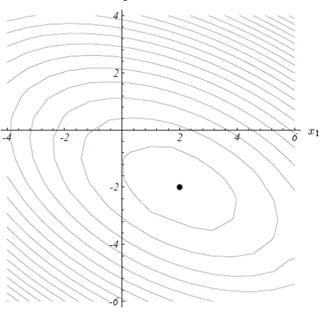
The quadratic form f(x) of the example is plotted in the following figure.
Figure 8: Quadratic form f(x)
The lowest point in figure 8 is the solution of the system A*x = b. In this sample problem that is x = [2, -2].
This can be seen more easily in the contour plot (figure 9).
2. Problem analysis
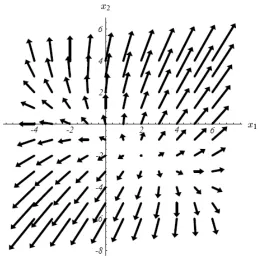
Figure 10: Gradient of f’(x)
De derivative of f(x) is defined as f’(x) and equals
f
'
(
x
)
=
A
x
−
b
The gradient points in the direction of the steepest increase of f(x). f(x) can be minimized by setting f’(x) to
zero.
2.2.2. Steepest Descent
The Steepest Descent method starts at an arbitrary point x(0) and every iteration a step is taken to get closer
to the solution of A*x=b. Every iteration will result in a better approximation. The number of iterations will
depend on the maximum error term specified and the speed of converge.
Every iteration i a step is taken in the direction where f(x(i)) decreases most quickly. This direction is the
opposite of f’(x(i)). This is equal to
−
f
'
(
x
(i))
=
b
−
A
x
(i), which is defined as the residual. The residualcan be described as the direction of the steepest descent.
For the example described above the starting point x(0) = [-2, -2] is chosen. Every iteration a step is made
along the direction of the steepest descent. This results in the following formula for the first iteration:
) 0 ( ) 0 ( ) 1
(
x
r
x
=
+
α
, where α determines the length of the step taken. In [3] αi is definedas
) ( ) (
) ( ) ( ) (
i T
i i T
i i
Ar
r
r
r
=
2. Problem analysis
Figure 11: Convergence of Steepest Descent
In figure 11 the convergence of steepest descent for the example problem is shown. In [3] αi is difined such
that the solid lines (in the direction of steepest descent) are orthogonal to each other. Summarizing the Steepest Descent method is described as:
)
2. Problem analysis
2.2.3. Conjugate Gradient
The idea behind Conjugate Gradient is the same as behind Steepest Descent but instead of multiple steps in the same direction, steps in CG are never in the same direction. Steps in CG are not orthogonal to each other but conjugate.
Conjugate Gradient algorithm:
)
In the context of this thesis it is to complex to describe the CG algorithm completely, see [3] for more details.
Figure 12: Convergence of Conjugate Gradient
2. Problem analysis
Unfortunately round off errors (because of floating point operations) result in accuracy loss. In chapter nine of [3] a convergence analysis of CG is done.
2.2.4. Complexity analysis
Variable α and β are scalars, d, r and x are vectors and A is a matrix. There is one initial step which
requires a sparse matrix-vector multiplication unless the initial vector x only contains zeros.
The computation cost of the iterative part can be divided into different classes: • One sparse matrix-vector multiplication
• Two inner products
• Three scalar vector multiplications • Three vector additions/subtractions
The properties of the matrix have great impact on the computational complexity. The number of MAC operations for the SMVM is equal to the number of non-zeros. For dense matrix vector multiplication the number of multiplications is equal to the size of the matrix and does not depend on the number of non-zeros. The more non-zeros, the more dominant the SMVM operation is. In case of the Volume
2. Problem analysis
2.3. Sparse Matrix-vector multiplication
In the conjugate gradient algorithm one of the operations is a sparse matrix-vector multiplication:A*x = y,
A is a sparse matrix, x is a dense vector and y is the dense result vector. This sparse matrix-vector
multiplication has to be calculated every iteration of the CG algorithm. Matrix A does not change during the algorithm only vector x changes.
2.3.1. Compressed Row Storage Format
The storage of a dense matrix with n rows and m columns requires the storage of n * m elements. In case of sparse matrices such storage scheme is very inefficient because most of the elements are zero. There are several other schemes to store sparse matrices. These schemes have one thing in common; they only store the non-zero elements. To prevent that the structure gets lost also the indices of the non-zero elements must be stored. The aim of these schemes is that multiplications with zero are not executed. Only the non-zero elements are multiplied with the corresponding elements of the vector. The corresponding elements of the vector can be accessed directly because the indices of the non-zero elements are stored. The most used format to store sparse matrices is the Compressed Row Storage (CRS) format.
CRS uses three vectors to store a sparse matrix. Vector ‘val’ contains all the non-zero elements. The order in which they are stored is row-wise. The vector ‘col’ contains the column index of each element stored in vector ‘val’. The vector row indexes the start of a new ‘row’ within the ‘val’ and ‘col’ vectors. Notice that there is an additional index in the ‘row’ vector to indicate the end of the last row.
Example:
(
)
(
)
(
1
3
4
6
7
)
row
1
4
3
2
3
4
col
val
1
2
3
4
5
6
6
0
0
0
4
5
0
0
0
3
0
0
0
0
2
1
=
=
=
⎟
⎟
⎟
⎠
⎞
⎜
⎜
⎜
⎝
⎛
=
A
Figure 13: Storage of matrix in Compressed Row Storage format.
With the following pseudo code the SMVM of a sparse matrix in CSR format can be computed:
for (int i=1; i =< n; i++)
for (int j = row(i); j < row(i+1); j++) y(i) = val(j)*x(col(j)) + y(i);
2. Problem analysis
2.4. FEM
Matrices
In chapter 2.1.2 the general properties of the system matrix were given. These general properties are: • The system matrix is sparse.
• The system matrix is symmetric.
• The system matrix can be reordered such that all non-zero values lie in a relative small band. Although the general properties hold for all the system matrices there can be quite some differences between them. At [11] a collection of system matrices is maintained. Implementations for SMVM are often benchmarked with these matrices. Besides these matrices this project focuses on the system matrix of the Volume Reconstruction algorithm, described in [1].
There is a lot of variation in the performance of current implementations for SMVM. These variations in performance are a direct result of the variations of the system matrices. This chapter addresses the differences in system matrices.
To classify the system matrices the following properties will be used: • Size of the matrix (n * n)
• Number of non-zeros • Sparsity of the matrix
This value indicates the number of non-zeros compared to the number of entries. • Bandwidth
Maximum difference in column index between the non-zero elements of one row. • Relative bandwidth
Ratio between n and the bandwidth. • Sparsity of the band
Indication on the number of non-zeros compared to the number of entries of the band.
2.4.1. Example of a regular system matrix
Figure 14: Structure plot of a regular system matrix
2. Problem analysis
The regular matrix bcsstk16 has the following properties:
Size 4,884 * 4,884
Non-zeros 290,378
Sparsity 1.2 %
Bandwidth 277 Relative bandwidth 5.7 %
Sparsity of the band 21.5 %
Table 1: Properties of regular system matrix bcsstk16
2.4.2. Example of a irregular system matrix
Figure 15: Structure plot of matrix bcsstk18
The matrix bcsstk18 (can be found at [11]) has the following properties:
Size 11,948 * 11,948
Non-zeros 149,090
Sparsity 0.1 %
Bandwidth 2,483 Relative bandwidth 20.8 %
Sparsity of the band 0.5 %
2. Problem analysis
2.4.3. System matrix of the Volume Reconstruction algorithm
Figure 16: Structure plot of the Volume Reconstruction system matrix
Size 138,324 * 138,324
Non-zeros 2,460,562
Sparsity 0.013 %
Bandwidth 22,393 Relative bandwidth 16.2 %
Sparsity of the band 0.079 %
Table 3: Properties of Volume Reconstruction system matrix
Figure 16 might give the impression that the sparsity of the band is quite high (high percentage). Figure 17 is a zoomed structure plot. From this figure it is clear that the sparsity of the band is low.
Figure 17: Zoomed structure plot of the Volume Reconstruction system matrix
2. Problem analysis
2.5. Field Programmable Gate Array
There are several hardware architectures to perform complex tasks. One of these hardware architectures is a Field Programmable Gate Array (FPGA). FPGAs are devices that have a high performance potential while maintaining high flexibility.
An FPGA is a device which has a lot of components. Often there are a lot of simple components such as 4-input LUTs (Look Up Tables) to implement for example AND, XOR, NOR or user defined functions, which are often combined with a flipflop. More complex components are for example the dedicated 18*18 bit multipliers and the dedicated memory blocks.
The components are connected through a programmable interconnect. Complex functions can be implemented by combining the standard components which is done by configuring the FPGA. An FPGA design is thus represented by a configuration file. The same FPGA can be used for different algorithms just by loading another configuration file. Further, the time to market of an FPGA design is short compared to an ASIC design.
Often it is not so hard to implement an algorithm onto an FPGA, developing an implementation that uses the full potential of the FPGA is however difficult.
2.5.1. MAC unit
For digital signal processing algorithms there are two common number representations, fixed point and floating point. Fixed point has a low hardware cost but a low precision while floating point is more
complex but has a high precision. For most digital signal processing algorithms, fixed point numbers have a sufficient precision. Because the hardware for fixed point operations is much simpler compared with floating point most of the digital signal processing algorithms are executed on fixed point hardware. Almost all the DSPs use fixed point numbers.
The Volume Reconstruction algorithm requires a high accuracy with a large range, fixed point hardware is thus not an appropriate choice. Within floating point, 32 and 64 bit are common widths. The Conjugate Gradient (CG) algorithm converges faster when higher accuracy is used [1]. The difference between the number of iterations CG needs to converge when using 32 or 64 bit floating point numbers is quite significant. Simulations have shown that the difference is roughly a factor two. The difference in the converge rate is caused by rounding off results. Rounding off numbers to 32 bit floating point numbers results in precision loss compared to 64 bit floating point numbers. The speedup in the number of iterations might justify the extra hardware cost of 64 bit floating point numbers compared to 32 bit floating point numbers see [1].
In[7] a 64 bit floating point MAC unit for an FPGA is presented. This MAC unit exploits the dedicated 18x18 bit multipliers that are present in the order of hundreds on current FPGAs. The 64-bit MAC unit presented in [7] uses nine 18x18 multipliers and has twelve pipeline stages to achieve high performances. The largest FPGA of the Virtex-II pro family from Xilinx, the XC2VP100 (in this project the target FPGA), can hold 31 of these 64-bit floating point MAC units running at 170 MHz (speed grade -6).
2.5.2. Processing Element
2. Problem analysis
completely on the algorithm what kind of combination of PEs gives the best performance. The choice is to have either a lot of simple PEs, a few complex PEs or a combination of simple and complex PEs.
Usually a design can be split into a number of PEs and a common part. The common parts are for example memories shared by PEs, busses shared by PEs, communication between PEs, etcetera. Some parts are only used by one PE. These parts are thus related to a specific PE. Often it is beneficial to have a memory block that is only used by one PE. The same holds for communication busses between memory and the MAC unit.
3. Design requirements
3.
Design requirements
In all known SMVM implementations the limiting factor is the available memory bandwidth. The complete matrix cannot be stored on the FPGA itself. The matrix has to be stored in external memory.
Thus to compute the SMVM, the matrix has to be transferred from external memory to the FPGA at least once. The main target of the design is to use the available memory bandwidth as efficiently as possible. The implementation of the SMVM thus has the following requirements:
• The design has to keep up with the memory interface; it should not become the bottleneck. • The overhead that might be needed to schedule the SMVM must be kept to a minimum.
Most of the memory bandwidth must be used to transfer the matrix and not to transfer overhead. • The design has to be scalable in the available memory bandwidth.
More bandwidth should mean a faster transfer and thus a faster computation. This implies that the utilization of the Processing Elements has to be reasonably high.
4. Previous work
4.
Previous work
There are many papers written on the implementation of Sparse Matrix-Vector Multiplication. Within the research field of SMVM there are two main directions. One direction tries to make a fast implementation on processors (GPP, Cell processor, VLIW processors); the other direction tries to make a fast
implementation on FPGAs. This chapter addresses three FPGA implementations with their strong and weak points.
4.1. Striping
based
implementation
A recent paper about a SMVM implementation is [10]. Their implementation uses a stripe method which was introduced by R. Melhem in [9]. The stripe method is discussed in chapter 4.4.
Strong points:
• Streaming based implementation Weak points:
• Utilization of implementation differs a lot because of the differences of the FEM matrices. • They never address the problems their method has and how they solved it.
• The performance of their implementation is not linear in the available memory bandwidth as can be seen in [12].
• They used benchmark matrices from [11], but forgot to index them.
4.2. Preprocessor
implementation
Another recent paper is [13], this implementation uses a preprocessing stage to compute the SMVM with a high utilization of the PEs. A major part of their implementation is discussed in chapter 5.
Strong points:
• High utilization of the PEs Weak points:
• Complete matrix stored on the FPGA. Matrices that do not fit on one FPGA need multiple FPGAs. • Complete result vector stored on FPGA.
• Implementation computes y = Ap * x, p≥1.
4.3. Straight forward implementation
A straight forward implementation is introduced in [14]. This method computes the SMVM directly with the standard CSR format.
Strong points:
• No preprocessing required
• Simple partial results adder implementation • No overhead
4. Previous work
Weak points:
• High utilization difference between multiplier and partial result adder (eight adders and only one multiplier)
• The performance of their implementation is not linear in the available memory bandwidth (because of the use of only one multiplier).
4.4. Stripe
method
The use of a systolic array to compute the matrix vector multiplication where the matrix has a dense band has proved its use in [8]. In [9] a method is described to compute the matrix vector multiplication where the matrix has a sparse band. The method described in [9] achieves higher efficiencies for sparse band matrices compared to [8].
Consider a sparse matrix vector multiplication A*x = y. A is a sparse matrix with bandwidth b, x is a dense
vector and y is the dense result vector.
In [8] to compute the matrix vector multiplication, b processing elements (PEs) are required. Each PE multiplies a straight-diagonal of A with the vector x. The efficiency of this approach is determined by the
sparsity of the band b. A dense band means a high efficiency and a sparse band will result in a low efficiency. As explained in chapter 2.4 the band of sparse matrices is often sparse.
R. Melhem explained in [9] a method to improve the low efficiency for Sparse Matrix-Vector
4. Previous work
4.4.1. Stripes
There are various ways to construct a stripe through a matrix for the coverage of the non-zero elements. In [10] a classification is given, increasing order (IO), strictly increasing order (SIO), strict-column increasing order (SCIO) and strict-row increasing order (SRIO). These classifications can be explained with regions. Each stripe is constructed in an iterative way, every iteration an element is added to the stripe.
Region of next element
Last added element of stripe
Region of next element Last added element of stripe
Figure 18 Figur 9
Figure 20 Figure 21
: Region of IO Stripes e 1 : Region of SIO stripes
Last added element of stripe
Region of next element
Last added element of stripe
Region of next element
: Region of SRIO stripes : Region of SCIO stripes
4. Previous work
The stripes in [9] are SIO and have thus the following properties: • A stripe contains at most one element of every row. • A stripe contains at most one element of every column.
• From the first property it follows that the longest stripe covers at most n elements. • Because of property one the elements on the same row are covered by different stripes.
The last property gives a lower bound on the number of stripes. The lower bound of the number of stripes is equal to the maximum number of non-zero elements on a row of the matrix.
In [10] a small modification on the region to construct stripes is proposed. The region is extended to be able to cover non-zero elements in the same column. This leads to SRIO stripes, which have almost the same properties as SIO stripes. The only difference is that a SRIO stripe can contain multiple elements of the same column.
Figure 22: Four SIO Stripes Figure 23: Two SRIO Stripes
The number of SRIO stripes is less or equal to the number of SIO stripes to cover all the non-zero elements [10] although they have the same lower bound on the number of stripes. Only SRIO stripes will be covered in the next chapters because they can give better results, see [10].
4.4.2. Construction of SRIO stripes
There are several ways to construct SRIO stripes. In [10] two types are described, top-down striping (TDS) and bottom-up striping (BUS). Both methods return the same number of stripes thus it is sufficient to only explain TDS. On each row a number of non-zero elements need to be covered by a stripe. TDS starts at the last non-zero element of the first row. The last non-zero element of a row is the non-zero element with the highest column index of that row. The non-zero element of the starting point is assigned to the first stripe. The second last element of the first row is assigned to the second stripe. These steps are repeated until the first element of the first row is assigned to a stripe.
TDS continues at the last element of the second row. If the column index of the element is larger or equal to the column index of the first stripe, it is assigned to the first stripe else it tries to assign it to a stripe with a column index smaller or equal to the column index of the element. The same is done with the second last element of the second row, etcetera.
4. Previous work
: Stripes constructed with TDS method
4.4.3. Systolic array
The method described in [10] uses a number of processing elements (PEs) together forming a systolic array. Each PE is able to compute a multiply accumulate.
I1 (x-values)
: Processing element of the systolic array
Figure 26: Systolic array for SMVM
4. Previous work
Each processing element has five inputs and two outputs.
The input I1 is for the x-values, I2 for the y-values and the group I3, I4, I5 for the stripe values (row index,
column index and value). Each PE has a local memory to hold the values of the stripe it processes. Vector x
and y stream through the system from right to left. In the initial case all the y-values are zero. Between PEs
the y-values are partial results and after the last PE the actual values are available. Communication between PEs is done through FIFO queues.
Each processing element processes a stripe. The first stripe is processed by the first PE, the second stripe by the second PE, etcetera. Figure 24 indicates the numbering order for the stripes, figure 26 indicates the numbering order for the PEs. The number of PEs is thus equal to the number of stripes to cover all the non-zero elements. The complete result vector y streams through the system once. A PE can either compute a
partial result and add it to an element of y or pass it to the FIFO of the next PE, this depends on the stripe
the PE is processing. If for example a stripe covers an element on the first row, the PE that processes the stripe will compute a partial result and add it to the first element of the result vector y and then passing it
on. If the stripe does not cover an element of the first row, the first element of the vector y will be passed
on without computing and adding a partial result. To compute a partial result a multiplication of two values is required, adding the partial result to an element of y takes an addition of two values. Each PE thus
requires a MAC unit to be able to perform these operations.
4.4.4. Utilization
To estimate the best case utilization of the MAC units the assumption is made that passing on an element to the next PE with or without computing and adding a partial result takes one clock cycle. This assumption implies that the MAC unit is fully pipelined. The result of the assumption is that the time to stream the result vector y through the system in the best case is equal to the length of the result vector y. In case of a
matrix A with size n x n, n clock cycles are needed to stream the result vector y through the system
regardless of the amount of partial results.
Suppose k stripes are required for the coverage of all the non-zero elements of a matrix. The systolic array would contain k PEs. In the ideal case n*k partial products could be computed and added to the result vector y. The number of partial products is equal to the number of non-zero elements. The utilization of the
best case scenario of the system can be computed with the formula: nnz/(n*k). nnz is the number of non-zero elements.
n is the size of the vector y.
k is the number of stripes and equal to the number of processing elements.
4. Previous work
Example one:
Matrix name: s3rmt3m
Size: 5,357 x 5,357
Non-zero elements: 207,123 0.72%
Stripes: 72
Figure 27: Structure plot of matrix s3rmt3m Figure 28: Utilization of PEs for matrix s3rmt3m
4. Previous work
Example two:
Matrix name: bcsstk18.mtx
Size: 11,948 x 11,948
Non-zero elements: 149,090 0.1%
Stripes: 216
Figure 29 Figure 30
Figure 31
: Structure plot of matrix bcsstk18 : Utilization of PEs for matrix bcsstk18
Because of the irregularity and sparsity within the band of matrix bcsstk18, the overall efficiency is only 5%.
Example three:
Matrix name: Volume Reconstruction matrix
Size: 138,324 x 138,324
Non-zero elements: 2,460,562 0.013%
Stripes: 555
: Utilization of PEs for Volume reconstruction matrix
4. Previous work
4.4.5. Cause of low utilization
The number of non-zeros a stripe covers directly influences the utilization of the PEs. To understand why the stripe method results in a low utilization for certain matrices, the construction process of a stripe has to be reviewed.
The following situation occurs frequently in the construction of stripes.
⎟
⎟
⎟
⎟
⎟
⎠
⎞
⎜
⎜
⎜
⎜
⎜
⎝
⎛
5 4 3
2 1
e
..
e
..
e
..
e
..
e
..
..
Figure 32: Part of a matrix
Figure 32 represents a part of a matrix, e1 till e5 represent non-zero elements. At a certain point stripe s1 is
constructed. The construction of a stripe is iterative; every iteration a non-zero element is added. Suppose the last added non-zero element added to s1 is e1. Because of the “construction rules” (region of next
element) e2 till e4 cannot be covered anymore by s1. After covering e1 the only element that could be
covered by the same stripe is e5. This yields in a low utilization of the PE that processes stripe s1, utilization
of s1 = 2/5 = 0.4.
The situation explained above occurs often with matrices of real problems. In the example above there are only three rows between e1 and e5. With matrices of real problems the distance between two elements
covered by a stripe are a lot larger (between 100 and 1000 rows). The utilization of these stripes is often less then 1%.
4.4.6. Conclusion
4. Previous work
4.5. Parallel Matrix Communication Network
In [6] a modification on the ideas in [9] is proposed. This modification leads to Parallel Matrix
Computation Network (PMCN). This method also uses a systolic array to compute the SMVM. In chapter 4.4.1 of this report a classification for stripes is given.
In the original idea of R. Melhem in [9], SIO stripes are used. In chapter 4.4 the modification of using SRIO stripes proposed in [10] is discussed. This modification leads to better results.
PCMN is also a modification of the stripe scheme. Instead of using SIO stripes, IO stripes are used. These IO stripes are also known as staircases. Instead of a stripe cover a staircase cover is used.
Examples:
Figure 33: Three SRIO Stripes Figure 34: Two IO Stripes / Staircases
In PCMN, the number of PEs is equal to the number of staircases. In general the number of staircases is lower than the number of SRIO stripes. The maximum length of a SRIO stripe is n (maximum number of non-zero it can cover), the maximum length of a staircase is 2*n-1.
4. Previous work
4.5.1. Parallel Matrix Computation Network - Example
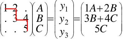
Consider the SMVM of matrix A with vector x. Vector x contains the values A, B and C.
The computation is represented in the following picture.
⎟⎟
Figure 35: Example of SMVM with staircases
The application considered in this report requires floating point representation. To achieve high performance, floating point MAC units are usually pipelined. In [7] a possible design of a 12 stage pipelined MAC unit is presented. The use of 12 pipeline stages results in a delay of 12 cycles. Without dependencies the delay does not play a role in the performance of the system.
To compute the SMVM of figure 35, one staircase is needed. In the first stage the PE starts the computation of a partial result of y1.
Cycle 1: ,
1
0
1
=
A
+
y
In the second stage it computes the second partial product of y1. The partial product has to be added to the
value of y1. Thus the second stage can only start when the result of the first stage is available. Because the
MAC unit has 12 pipeline stages, the second stage can not start before cycle 13. Cycle 13:
y
1=
2
B
+
y
1,The same analysis can be done for then rest of the computations. Stage three can immediately start because there are no dependencies. Cycle 14:
y
,2=
3
B
+
0
Cycle 26:
y
2=
4
C
+
y
2,Cycle 27:
y
3=
5
C
+
0
4. Previous work
4.5.2. SIO Example
Figure 36
: Example of SMVM with SIO stripes
Stripe one is defined as the solid line, stripe two is defined as the dashed line. Processing element one processes stripe one and PE two processes stripe two. A detailed description of the systolic array can be found in chapter 4.4.3.
Timing analysis of the example for PE one:
In the first clock cycle, PE one passes value A to PE two. Cycle 1: Pass value A to next PE.
In the second clock cycle it starts the computation of a partial result of y1.
Cycle 2: ,
2
0
1
=
B
+
y
In the third clock cycle it starts the computation of a partial result of y2.
Cycle 3:
y
2,=
4
C
+
0
In the fourth clock cycle it passes on value y3.
Cycle 4: Pass value y3 to next PE.
Timing analysis of the example for PE two:
In the first stage of PE two it has to compute a partial result of y1. PE two can only start this computation
after it has received the partial result y1’ from PE one. Thus PE two cannot start before cycle 14 (2+12).
Cycle 14:
y
1=
1
A
+
y
1,The second stage a partial result of y2 is computed. Because of the dependencies, this computation cannot
start before cycle 15 (3+12). Cycle 15:
y
2=
3
B
+
y
2,The last stage starts at cycle 16. Cycle 16:
y
3=
5
C
+
0
To obtain the highest possible efficiency, the system continuously has to calculate SMVMs. This can be done by multiplying the matrix with multiple vectors. This optimization can be used in the overall
4. Previous work
4.5.3. Conclusion
PMCN is introduced by the inventors as a better method to compute SMVM than the method of Melhem. The analysis in [6] to support their claim is very abstract and does not relate to a possible hardware implementation. PMCN and the method of Melhem are both projected onto an example in this report. PMCN needed less hardware but more clock cycles to compute the SMVM. The efficiency of PMCN was only 18.5% for this example while the solution of Melhem achieved an efficiency of 62.5%.
5. Alternative 1: Plans
5.
Alternative 1: Plans
5.1. Computing the SMVM on one PE
In chapter 2.5.1 it is already indicated that the number of MAC units that the target FPGA can hold is 31. This chapter explains the implementation of a PE and possible optimizations to give a base for a multiple PE design.
5.1.1. Plans
As explained in chapter 2.5.2 a PE is able to perform MAC instructions. This means that the complete SMVM can be executed on one PE. The following pseudo code represents a normal (not sparse) matrix vector multiplication of matrix A times vector x and the result is vector y. Matrix A has n * n elements.
for (int i = 1; i < n; i++) {
The outer for loop loops over the rows and the inner for loop loops over the columns. In case of a sparse matrix the inner loop is modified such that the loop is only over the non-zero elements.
The problem with this schedule is that the pipeline stages of the MAC unit will result in a delay because of the dependencies of value y(i). For the following example the number of pipeline stages of the MAC unit is assumed to be one.
Figure 37: Example SMVM
In cycle one the PE can start the computation of y1’=1A+0. The problem is that the PE cannot start the
computation of y1=2B+ y1’ at cycle two because y1’ is not yet available because of the pipeline latency. The
PE can only start at cycle three. Thus for the first row, one MAC slot is not used. In [13] a method is described to use the MAC unit more efficiently. This is done by computing multiple results at the same time. For this particular example at cycle one the PE can start the computation of y1’=1A+0, at cycle two
y2’=3B+y2, at cycle three y1=2B+ y1’, at cycle four y2=4C+ y2’ and at cycle five y3=5C+y3. With this
schedule the utilization of the MAC unit is 100%. This optimization is also known as loop unrolling. The following pseudo code represents this scheme for dense matrices:
for (int i = 1; i < n; i=i+2) {
5. Alternative 1: Plans
longest rows (most non-zero elements) first. In case of the MAC unit proposed in [7] the adder pipeline has eight stages. This means that eight rows will be processed in parallel.
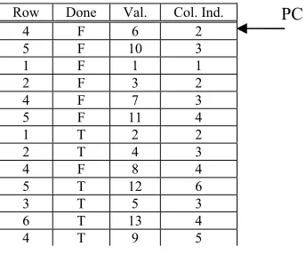
As explained before a near optimal schedule can be achieved by processing the longest rows (with the most non-zero elements) first. Further each non-zero element has a column index which must be used to index the vector and an additional boolean to indicate the completion of the computation of a row. All these variables can be seen as a plan to compute the SMVM in a near optimal way. In the FPGA this “plan” is stored in a memory. Further a PE also needs a memory with the vector x and a memory to store the result
vector y.
Consider the following more complex example with an adder pipeline of four stages.
⎟
From the matrix and the number of pipeline stages the following plan can be constructed.
Row Done Val. Col. Ind.
: "Plan" for the computation of SMVM of the example
For simplicity the column row is added to the plan. A near optimal schedule can be constructed by starting with the longest row. In this example row number four is the longest (most non-zero elements) so it is scheduled first. It does not matter which non-zero element is processed first. It makes sense to just start with the left most non-zero element; in this case it has the value six. The column index of the non-zero element is two. Because this is not the last non-zero element of the row, the value of done is false. Summarized, the first row of the plan has the values 4, false, 6 and 2. Because of the adder pipeline the second non-zero element of row four is processed at row five of the plan. The second row of the plan will be occupied by the first non-zero element of the second largest row, etcetera. Incase of equally long rows (same number of non-zero elements) it does not matter which one is scheduled first.
5. Alternative 1: Plans
5.1.2. PE Design
Figure 40 represents the design of the PE for execution of plans as suggested in [13].
Val. A B C D E F
Vector x PC Row Done Val. Col. Ind.
4 F 6 2 5 F 10 3 1 F 1 1 2 F 3 2 4 F 7 3 5 F 11 4 1 T 2 2 2 T 4 3 4 F 8 4 5 T 12 6 3 T 5 3 6 T 13 4 4 T 9 5
0
Res. .. .. .. .. .. .. F T
enable address
Figure 40: PE design
For simplicity the four pipeline stages are placed outside the adder and implemented as four registers. The column Col. Ind. is used to index the vector x. The column Row is used to index the result memory.
5.1.3. Mapping of the system matrix
5. Alternative 1: Plans
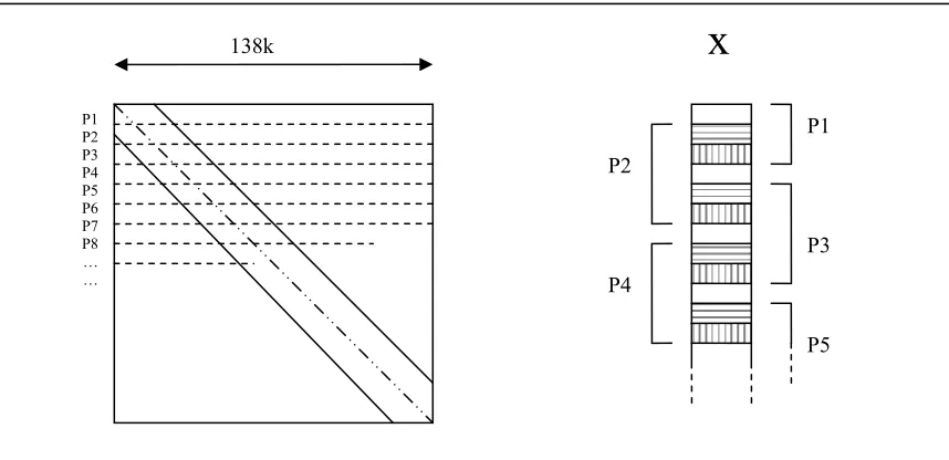
The following enumeration recapitulates the properties of the application matrix. The numbers are approximations.
• Non-zero elements: 2,5M • Size: 138k x 138k • Bandwidth: 22k
• Average number of non-zero elements per row: 20
The application requires 64-bit values and the number of non-zeros of the matrix is about 2,5M, this means that the storage of one plan for the complete SMVM requires at least 2,5M * 64 = 160 Mbit. The largest Virtex-II pro FPGA, the XC2VP100, has only 7,992 Kbit. Thus to compute the sparse matrix vector multiplication, the original plan has to be split into multiple smaller plans. On average there are twenty non-zero elements on each row. If the complete memory of the FPGA would be used to store only the values of a plan than approximately (7,992*1024)/(64*20) ≈ 6400 rows could be covered. The matrix has approximately 138k rows. To cover all the 138 rows of the matrix, at least ┌(138k/6400) = 22 plans are required and hence 22 FPGAs. Besides the storage of the values of the matrix, the values of the vector must be stored, the result values and indices to index the memories. The value of 22 is a lower bound on the total number of plans.
The complete storage of the vector x would require 138k*64 ≈ 8,700 Kbit, which is more than the largest
Virtex-II pro has available as memory. A plan that covers the complete matrix requires the complete storage of the vector x. The conclusion from the previous paragraph was that the coverage with one plan is
not possible because of the limited amount of memory of current FPGAs. Several smaller plans are
required to cover the matrix. A plan can be defined as a strategy to compute a part of the SMVM by one PE such that the storage does not exceed the local memory of the PE.
Construction of a plan can be done is several ways. If the rows a plan covers can be any row of the matrix, every plan requires storage of the complete vector x, which is not possible. A better idea is that a plan only
covers consecutive rows. The advantage is that only a part of the vector x has to be stored.
Figure 41: Dividing the matrix into “plans”
138k
P1 P2 P3 P4 P5 P6 P7 P8 … …
x
P1 P2
P3 P4
P5
The bandwidth of the matrix is approximately 22k elements. Each plan can index the number of rows it covers plus the size of the bandwidth. The upper bound on the number of rows a plan covers is 6400. This would require (6400+22k)*64 ≈ 1818 Kbit of storage for the vector x for each plan.
Until this point all the computations where performed with an upper bound on the number of rows a plan could cover on average. The computations where only based on the storage of the values in the plan. To index the complete vector x, 18 bits are required. But a plan only has to index a part of the vector x. The
5. Alternative 1: Plans
For the boolean value Done, one bit is required. In a real implementation the column row is not present. Instead an additional memory is used to index the results, which is discussed later. For each non-zero element 64+15+1 = 80 bits are required. The number of results is equal to the number of rows a plan covers. The upper bound is 6400*13 ≈ 82 Kbits.
The memory to index the results will be kept constant; the other parts will be variable with the number of rows. Solving the following formula gives a more realistic idea on the average number of rows a plan covers.
On average each row has twenty non-zero elements, for each non-zero element 80 bits are needed. The size of a plan is thus the number of rows times the average number of non-zeros times 80 bits.
bits
The number of elements for the storage of a part of vector x is the number of rows a plan covers plus the bandwidth.
To compute the complete SMVM on one PE multiple plans are needed. The memories in FPGAs are often implemented as true dual port. This means that there can be two processes reading or writing at the same time if not on the same address. The PE executes a plan in order, thus after it has processed a non-zero element it can be overwritten by a non-zero element of the next plan. Suppose a PE processes a non-zero element every clock cycle and every clock cycle a new non-zero element can be loaded into memory. If this is the case than loading a plan takes the same amount of time as executing a plan. Switching from one plan to another does not require extra clock cycles.
A plan requires a certain part of the vector x available in memory. Suppose a PE is executing plan pd. To
execute this plan part vecd of the vector x has to be in memory. After the PE has executed the last non-zero
element of plan pd it switches to plan pd+1. Plan pd+1 requires part vecd+1 of the vector x to be in memory. To
guarantee that switching to another plan does not take any additional clock cycles the parts vecd and vecd+1
must be in memory at the same time. The size of vecd is about 26k elements. The total length of the vector
x is 138k elements.
The size vecd is thus 10% of the size of the vector x. The total number of parts of the vector x is equal to the
number of plans which is 35. The conclusion is that the part vecd has overlap with the previous part (vecd-1)
and the next part (vecd+1).
For this example the number of rows a plan covers is 4k with on average 20 non-zero elements on each row. Further there are three external memories, one holding the plans, another holding the vector x and one
to store the result vector. There are three memory interfaces to the three external memories. One memory interface is used to load plans into the internal memory of the FPGA by overwriting the already loaded plan. Another memory interface will be used to store the results into external memory and the last memory interface is used to load parts of the vector x.
Suppose the first plan p1 and vec1 are loaded into memory. The PE starts executing the first plan. While the
PE is processing plan p1 plan p2 will be loaded by overwriting the non-zero elements that already have been
processed. At the same time vec2 has to be loaded into memory. Because of the overlap with vec1 it is
5. Alternative 1: Plans
vector x
0 26k
vec1
30k 4k
vec2
8k 34k
vec3 Figure 42: Dividing vector x into parts
In the time the PE is executing plan p1, 4k elements of vec2 have to be loaded into memory. The number of
non-zeros of a plan is equal to 20*4k = 80k. Thus the memory interface for loading new plans must have a higher bandwidth than the memory interface used for loading parts of vector x. The difference is a factor
twenty.
5.1.4. FPGA implementation
FPGA
PC
Figure 43: FPGA implementation
The memory bandwidth requirements for this system are very high. The question is if this system could be optimized such that the utilization of the PE stays at 100% while using less memory bandwidth.
MAC Plan
4k rows 80k non-zero
elements
Vec
d + vec
d+1
Plans External mem
Result External mem
Result
m
5. Alternative 1: Plans
5.1.5. Possible optimization
In the above examples the SMVM used only one vector. Each non-zero element is processed only once. A plan consisted of 80k non-zero elements that could index 26k elements of the vector x. This implies that
elements of the vector x are indexed more than once.
Loading data from external memory is very costly. The idea is thus to use the data that is already on chip as much as possible. The size of a plan is very large compared to the size of the vector. Executing a plan multiple times would decrease memory bandwidth requirements. This can be done if there are multiple vectors that must be multiplied with the same matrix.
Suppose there are five vectors that must be multiplied with the same matrix. In the first run the PE executes plan p1 with vector one, in the second run it executes p1 with vector two, in the third run it executes p1 with
5. Alternative 1: Plans
Figure 44: FPGA implementation with multiple vectors
In the original scheme where the SMVM was only executed with only one vector, there was only one memory to hold the plan. This was possible because the new plan could directly overwrite the old plan with the same speed the PE executed. This requires a high memory bandwidth. The advantage of multiplying with multiple vectors in parallel is that the bandwidth requirements are lower. For this particular example the time to load a new plan may be five times longer than the time the PE would execute the plan. However a new plan cannot overwrite the plan the PE is executing. A solution is to use two memories of the same size that alternate their function. The memories can either be used by the PE to execute the plan or it can be used to store the new plan from external memory.
The gray boxes in figure 44 are not active for the execution of the plan.
The consequence of the additional memories is that there is less memory available for a plan. The number of plans will increase and the number of rows a plan covers will decrease.
5. Alternative 1: Plans
⎡
138
/
⎤
500
276
640
3200
110
64
=
=
≈
−
≥
+
+
×
rows plans
rows
rows rows
result FPGA
N
k
N
N
k
N
N
S
S
This chapter explained an algorithm to compute the SMVM on one PE. The PE was defined as a unit which had only one MAC unit to perform computations. From this definition an algorithm was proposed which achieved a very high utilization of the MAC unit with a limited requirement on the memory bandwidth. The utilization of the MAC unit was not addressed formally because simulations have shown that with a relative high number of rows (in the order of 1000) the lower bound of the utilization was 99%.
5. Alternative 1: Plans
5.2. Computing the SMVM on Multiple PEs
The largest Virtex-II pro FPGA can hold 31 MAC units, which run at 170 MHz [7]. The peak performance of this FPGA with this type of MAC unit is 31*170M*2 = 10,5 MFLOPS (double precision). In the previous chapter only one MAC-unit was used which means that at most 1/31 of the peak performance of the FPGA was used. Using more MAC units might achieve better results. In this chapter as well as the previous, the PEs are specified to only have one MAC unit to perform computations.
5.2.1. Introduction
In the previous chapter the idea of plans was explained. A PE executes a plan on a vector or multiple vectors, loads new plans and loads elements of vectors. Figure 43 is taken as a base for a multiple PE design.
Assume a design with four PEs that all execute plans and there are 200 plans to compute the SMVM. The first fifty plans could be assigned to the first PE, plans 51 till 100 can be assigned to the second PE, etcetera.
Results Results Results Results
Figure 45: Possible four PE implementation
For every additional PE, two additional memory interfaces are required. But this isn’t the largest
disadvantage. To store a part of the vector x, at least 22k elements must be stored because of the bandwidth of the matrix. These elements are represented with 64 bits, 22k*64 ≈ 1400 Kbits. This is already 20% of the available memory of the FPGA. Thus at most five PEs could be used with this scheme. An optimization would be to only store the elements of the vector x that are really going to be used by a plan. Table 4 shows
5. Alternative 1: Plans
Number of rows a plan covers
Number of elements of vector x for a
plan
Avg. Number of elements of vector x really
used
Percentage Max number of elements really used by a plan
32 32+22k 232 1.1% 1080
64 64+22k 402 1.8% 1698
128 128+22k 707 3.2% 2468
256 256+22k 1222 5.5% 3235
512 512+22k 2088 9.0% 3799
Table 4: Element usage of the Volume Reconstruction matrix
In the preprocessing phase where the plans are made, also the indexes of the elements of the vector x that
are needed by a plan could be saved. Thus if a plan covers for example 128 rows, it covers on average 128*20 = 2560 non-zero elements and needs on average 707 elements of the vector x. For each plan the
indexes of the 707 elements can be stored. Loading a new plan means now loading a plan and loading the values of the vector x needed by the plan.
Switching from one plan to another should not cost any additional cycles. Thus two memories are needed for the storage of the vector x. Both memories alternate their function; a memory is either used to load new
values or to provide the PE with the value indexed by the plan. In the ideal case executing a plan should take longer than loading new elements. For the example above where a plan covers 128 rows, executing the plan takes at least 2560 (128*20) clock cycles. A realistic assumption about the memory bandwidth is that every clock cycle an element of the vector could be loaded. With that assumption one memory interface has sufficient bandwidth to support three PEs. The aim is to use as much MAC units as possible; the maximum number of MAC units that could be implemented is 31 [7]. This would require ┌(31/3) = 11 memory interfaces for loading elements of the vector x.
An element of the vector x may be used in several plans. Plans that use the same element of the vector lie
often next to each other. If the PEs share a bus that streams the elements of the vector x, each PE can copy
an element into its own local memory when it needs that element. Suppose there is a system with four PEs, taking advantage of the shared bus means that they have to execute plans close together. For example PE 1 will execute plan 1, PE 2 will execute plan 2, etcetera. Thus in the first run the first four plans are mapped onto the four PEs. In the second run plan 5 till 8 will be mapped, etcetera. Suppose each PE executes plans each covering 128 rows. If the PEs do not share a bus, on average 4*707 = 2828 elements of the vector x must be loaded for each run. In case of the shared bus it is on average 2088 elements (4*128 = 512), an improvement of 26%. Eight PEs executing plans that cover 32 rows, results in loading 8*232 = 1856 elements without a shared bus or loading 1222 elements with a shared bus. This is an improvement of 34%. This effect is illustrated in Table 5.
PEs Rows per Plan Without shared bus With shared bus Improvement
4 128 2828 2088 26%
8 32 1856 1222 34%
8 64 3216 2088 35%
16 32 3712 2088 44%
5. Alternative 1: Plans
Summarized, each PE has two small local memories for storage of elements of the vector x, the memories
alternate their function, a memory is either used by the PE to execute the plan or to store new elements of the vector x. Further the PEs share a bus for loading the elements.
Elements
x
Elements
x
Sel.
MAC 1 Sel. Index
Plan PE 1 PE 1
Elements
x
Elements
x
Sel.
MAC 2 Sel. Index
Plan PE 2
PE 2 PE 3
: Vector optimization Figure 46
The index block is a memory that is used to indicate whether an element on the shared bus must be stored or not, this depends on the plan. The values of the index memory are determined by the plan.
As already explained in chapter 5.1 where the SMVM is computed with only one PE, it is not efficient to execute a plan only once. It is better to execute a plan on multiple vectors. In chapter 5.1.5 a construction is proposed to load a plan with a lower speed than a PE would execute it. For multiple PEs this advantage can be used to load new plans for all the PEs with only one memory interface. This requires two memories for the storage of the plans plus two memories for the storage of Index values.
5. Alternative 1: Plans
Elements
x
Elements
x
Sel.
MAC Sel. Index
Plan PE PE
Plan PE
Loa
d plan Sel.
Sel.
Resu
lts
Resu
lts
Store results Elements of vectors
Results
Index
5. Alternative 1: Plans
5.2.2. FPGA implementation
This section illustrates the architecture for a complete SMVM design with three PEs.
Figure 48: Possible three PEs implementation
PE 1 PE 2 PE 3
Load Elements Vectors
External Mem.
L
oad
P
lan
s
Plans External Mem.
Results
Sto
re resu
lts
FPGA
This design uses three memory interfaces, one to load the plans, one to load elements of vectors and one to store the results. The number of PEs determines the bandwidth requirements of the memory interfaces. Having more PEs means a larger vector to be loaded and more results per clock cycle.
5. Alternative 1: Plans
The bottleneck of a SMVM is always the memory bandwidth. The proposed algorithm has some
optimizations to use the available memory bandwidth more efficiently. It is also scalable in terms of more memory interfaces. The following scheme gives an idea how to use four memory interfaces.
Figure 49: Four memory interface implementation
PE 1 PE 2 PE 3
Load Elements Vectors
External Mem.
L
oad
P
lan
s
Plans External Mem.
Results
Sto
re resu
lts
External Mem.
FPGA
PE 4 PE 5 PE 6
Load Elements Vectors
External Mem.
The gray colored parts are the parts that where also present in the design with three memory interfaces, the black colored parts are new. In this example PE 4 till PE 6 will execute the plans of PE 1 till PE 3 on multiple other vectors. By sharing plans between PEs the memories of the FPGA are used more efficiently.
5.2.3. Conclusion
To get the most out of the FPGA the following optimizations were proposed:
Optimization Result Only store elements of vector really needed Efficient use of memory
Needed to implement more than 5 PEs (see section 5.2.1)
Using a shared bus to load elements of vector Lowers the requirements of the memory bandwidth Multiplying with multiple vectors Lowers the requirements of the memory bandwidth More memory interfaces Using memory more efficiently
5. Alternative 1: Plans
Now the complete design is specified a few definitions are made to explain the preprocessing phase more easily:
• A global vector is the vector of the SMVM.
• A local plan is a schedule used to achieve high utilizations of a MAC unit. A local plan is executed
by one PE. For each local plan there is a local vector.
• The local vector contains only the elements of the global vector required by a local plan.
• A super plan is a collection of local plans that are executed in parallel on multiple PEs. Each super
plan has a super vector.
• A super vector contains all the elements of the collection of local vectors.
• A local vector is thus a subset of a super vector and a super vector is a subs


![Figure 40 represents the design of the PE for execution of plans as suggested in [13]](https://thumb-us.123doks.com/thumbv2/123dok_us/1041709.1129875/39.612.102.353.140.524/figure-represents-design-pe-execution-plans-suggested.webp)