An FPGA Implementation of Energy Efficient
Code Converters Using Reversible Logic
Gates
Rakesh Kumar Jha
1, Arjun singh yadav
2Assistant Professor, Dept. of ECE, Corporate Institute of Science & Technology, Bhopal, India1
PhD Scholar, Dept. of ECE, MANIT, Bhopal, India2
ABSTRACT:Reversible Logic has turned out to be one of the promising computing technologies assuring zero power dissipation. It has a wide spectrum of applications like Low Power VLSI, quantum computing, Bio Informatics Optical Circuits and Nanotechnology based systems. In this paper 4 bit reversible comparator based on classical logic circuit is represented which uses existing reversible gates. In this design we try to reduce optimization parameters like number of constant inputs, garbage outputs, and quantum cost. The results show that, the proposed comparator has 4 quantum cost and one constant input less than the prior design.
KEYWORDS: Reversible gates; reversible comparator; quantum cost; constant inputs; garbage outputs I. INTRODUCTION
Researchers like Landauer and Bennett have shown that every bit of information lost will generate kTlog2 joules of energy, whereas the energy dissipation would not occur, if computation is carried out in a reversible way. k is Boltzmann’s constant and T is absolute temperature at which computation is performed. Thus reversible circuits will be the most important one of the solutions of heat dissipation in Future circuit design. Reversible computing is motivated by the Von Neumann Landauer (VNL) principle, a theorem of modern physics telling us that ordinary irreversible logic operation which destructively overwrite previous outputs)in cur a fundamental physics) that performance on most applications within realistic power constraints might still continue increasing indefinitely. Reversible logic is also a core part of the quantum circuit model.
II. LITERATURE SURVEY
In this paper we implement 4 Bit reversible logic and compare it with classical 4 bit comparator circuit. We have studied many authors in the field for idea about reversible logic and how it functions. The base paper is “Energy efficient code converters using reversible logic” by Mr. M. Saravanan and Dr. K. Suresh Manic [3]“. we modified few designs and then implemented it using VHDL. For reversible logic functioning we have studied Irreversibility and Heat Generation in the Computing Process by R. Landauer [1] and “Logical Reversibility of Computation,” by C.H. Bennett[2].
III
.
BASIC REVERSIBLE LOGICA. Terminologies
Some of the basic terms used in reversible logic is described below:-
Definition 2: Reversible Logic Gate -A reversible logic gate is an N- input N-output logic device that provides one to one mapping between the input and the output. It not only helps us to determine the outputs from the inputs but also helps us to uniquely recover the inputs from the outputs.
Definition 3: Garbage Outputs (GO) - Additional outputs can be added so as to make the number of inputs and outputs equal whenever necessary. The numbers of outputs which are not used in the synthesis of a given function are called garbage outputs. In certain cases these become mandatory to achieve reversibility.
Definition 4: Quantum Cost (QC) - This refers to the cost of the circuit in terms of the cost of a primitive gate. It is computed knowing the number of primitive reversible logic gates (1 * 1 or 2*2) required to realize the circuit.
Definition 5: Gate levels or Logic Depth- This refers to the number of levels in the circuit which are required to realize the given logic functions.
Definition 6: Flexibility - This refers to the universality of a reversible logic gate in realizing more functions.
Definition 7: Gate count (GC) - The number of reversible gates used to realize the function.
Definition 8: Constant Inputs (CI) - These refer to the
number of inputs that are to be maintained constant (either at 0or 1) in order to synthesize a given logic function.
Definition 9: Total LogicalCost - This is measured by
counting the number of AND operations, number of EX-ORoperations and number of NOT operations.
LetA = No. of EX-OR operations B = No. of AND operations C = No. of NOT operations
Then the total logical cost T is given as sum of number ofAND, EX-OR and NOT operations. T= N (A).A+ N (B).B+ N (C).C
Where N (*) denotes "number of' gates.
Definition 10: Total reversible logic implementation
Cost (TRLIC) - This parameter is defined as the sum of all the cost metrics of a reversible logic circuit viz,. the CI, GC, QC and GO. The TRLIC is a parameter which reflects the overall performance of a reversible logic circuit.
TRLIC=∑ (CI, G C, QC, G O)
B.Basic reversible Logic Gates
The basic reversible logic gates that are widely studied inthe reversible logic are shown below.
1. 1x1 NOT GATE : 1×1 NOT gate, which has the zero quantum cost, is demonstrated in Fig. 1.
Figure1 .1x1 NOT Gate
2. N-bit Controlled-Not Gate
Figure2. N-bit controlled NOT gate
3. Feynman Gate:
It is a 2x2 gate with quantum cost of one. It is also
Called Controlled NOT (CNOT) gate depicting its operation;i.e., it can be used to obtain the output in its true form orcomplemented form by controlling the first input.
Figure 3.Feynman Gate 4. Peres Gate
It is a 3x3 gate that has input output combination
as (A- P = A, B- Q = A xor B, C- R = AB xor C. It is the only 3x3 gate with least quantum cost of 4. It can be used to obtain the product of two input bits.
Figure 4.Peres Gate
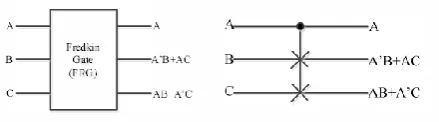
5. Fredkin Gate:
It is also a 3x3 gate [4] which maps inputs (A, B, C)
to output (A, A'B+AC, A'C+AB). It has a quantum cost of five and is a parity preserving gate as well as a universal gate.
6. Toffoli Gate:
It is a 3x3 gate [4] with input output mapping givenby (A-P = A, B- Q = B, C- R= AB xor C). It has a quantum cost of five and is also a universal gate. Its gate diagram and quantum circuit are as shown in the
figure.
Figure 6.Toffoli Gate
7. TR gate
Figure 7 shows TR gate. Its input and output mapping is given by (A-P = A, B- Q = B, C- R= AB’ xor C). Its new quantum implementation,. The quantum cost of this gate reduces to 4 by this new quantum implementation. Earlier, the TR gate quantum cost was estimated as 6 .
Figure 7.TR Gate
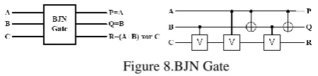
8. BJN gate
The gate is shown in figure 8 and its quantum cost is 5.its input output mapping is given by (A-P = A, B- Q = B, C- R= (A+B) xor C).
Figure 8.BJN Gate
9. URG gate
The gate is shown in figure 9 and its input output mapping is given by (C xor ABP, BQ, C xor (A+B)R).
Figure 9.URG Gate
10. HNG gate
IV. PROPOSED REVERSIBLE CODE CONVERTER
Designing of reversible logic circuit is challenging task, since not enough number of gates are available for design. Reversible processor design needs its building blocks should be reversible in this view the designing of reversible code converters became essential one. A code is basically the pattern of these 0’s and 1’s used to represent the data. Code converters are a class of combinational digital circuits that are used to convert one type of code in to another.Some of the most prominently used codes in digital systems are Natural Binary Sequence, Binary Coded Decimal, Excess-3 Code, Gray Code, ASCII Code etc.
V. REVERSIBLE BINARY TO GRAY AND GRAY TO BINARY CODE CONVERTER
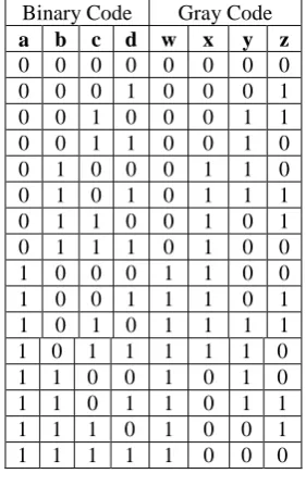
Binary to Gray code converters used to reduce switching activity by achieving single bit transition between logical sequences. If Input vector is I(D,C,B,A) then the output vector O (Z,Y,X,W). The circuit is constructed with the help of Feynman Gate (FG) .The figure 11 shows the circuit diagram of reversible Binary to Gray code converter & Gray to Binary code converter.
Figure11. Circuit diagram of Reversible Binary to Gray code converter.
The output of the circuit is gray code of input which is given in table 4.1 below.
TABLE 4.1: Truth Table of B2G converter
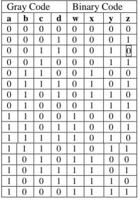
Reversible Gray to binary converter is constructed using FG gate as shown in figure 12. If Input vector is I(D,C,B,A) is in gray code then the output vector O (Z,Y,X,W) is its binary values.
Binary Code Gray Code
a b c d w x y z
Figure12. Circuit diagram of Reversible Gray to Binary code converter.
The binary equivalent of gray code is shown in table 4.2 below.
Gray Code Binary Code
a b c d w x y z
0 0 0 0 0 0 0 0 0 0 0 1 0 0 0 1 0 0 1 1 0 0 1 0 0 0 1 0 0 0 1 1 0 1 1 0 0 1 0 0 0 1 1 1 0 1 0 1 0 1 0 1 0 1 1 0 0 1 0 0 0 1 1 1 1 1 0 0 1 0 0 0 1 1 0 1 1 0 0 1 1 1 1 1 1 0 1 0 1 1 1 0 1 0 1 1 1 0 1 0 1 1 0 0 1 0 1 1 1 1 0 1 1 0 0 1 1 1 1 0 1 0 0 0 1 1 1 1
TABLE 4.2: Truth Table of G2B converter
VI. FPGA IMPLEMENTATION
VHDL implementation of in Energy Efficient Code Converters using Reversible Logic Gates vlsi chips using EDA tool Xilinx’s 8.2i, and simulation is done on Modelsim 6.3F. The RTL (register transfer level) of code converter is shown is below.
Figure 13. RTL of Gray to Binary code converter.
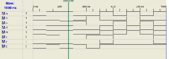
VI. SIMULATION RESULTS AND ANALYSIS
The simulation is done on ise simulator and described below. The circuit converts the binary number to its equivalent gray code. Similarly gray to binary conversion is simulated.
Figure14.
Simulation result of Binary to Gray conversionFigure15. Simulation result of Gray to binary conversion
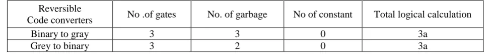
VII. CONCLUSION
The proposed reversible code converter is more efficient than the conventional code converters. Evaluation of the proposed circuit can be comprehended easily with the help of the Table 7.2. The total logical operation involved in the proposed reversible code converter circuit is calculated with the help of following logical assignments
Reversible
Code converters No .of gates No. of garbage No of constant Total logical calculation
Binary to gray 3 3 0 3a
Grey to binary 3 2 0 3a
TABLE 7.2 Comparative results of different reversible logic circuits
REFERENCES
[1] Landauer R, “Irreversibility and Heat Generation in the Computing Process,” IBM Journal of Research and Development, vol. 5, no. 3, pp.
183- 191, July 1961.
[2] Bennett C.H “Logical Reversibility of Computation,” IBM Journal of Research and Development, vol. 17, no. 6, pp. 525-532, November
1973.
[3] Saravanan ,M and Manic Suresh , K “Energy Efficient Code Converters Using Reversible Logic Gates”Proceedings of 2013 International
Conference on Green High Performance Computing.
[4] . Haghparast, M , Rezazadeh , L,and . Seivani, “ V Design and Optimization of Nanometric Reversible 4 Bit Numerical Comparator,” Middle-East Journal of Scientific Research, vol. 7, no. 4, pp. 581-584, 2011.
[5] Thapliyal, H. , Ranganathan . N , and Ferreira. R, “Design of a Comparator Tree Based on Reversible Logic,” in Proc. 10th IEEE
International Conf. on Nanotechnology, Korea, 2010, pp. 1113-1116.
[6] Thapliyal H. and Ranganathan, N. “Design of Efficient Reversible Binary Subtractors Based On a New Reversible Gate,” IEEE Computer
Society Annual Symposium on VLSI (ISVLSI), Florida, 2009, pp. 229–234.
[7] . Nagamani, A. N , Jayashree, H. V. and Bhagyalakshmi, H. R. “Novel Low Power Comparator Design Using Reversible Logic Gates,”