Simulation Results Analysis Of Basic And Modified RBSD
Adder Circuits
1Sobina Gujral, 2Robina Gujral Bagga
1Assistant Professor Department of Electronics and Communication,
Chandigarh University, India
2
Assistant Professor Department of Electronics and Communication, MVJ College of Engineering, India
Abstract: Adders are the key element of the arithmetic
unit, especially fast parallel adder. Redundant Binary Signed Digit (RBSD) adders are designed to perform high-speed arithmetic operations. The RBSD Number System is gaining popularity due to the properties of carry-free addition / subtraction. In computational environment it is not convenient for manual computations but useful in designing high-speed arithmetic machines. This number system eliminates the carry / borrow propagation chains which reduces the computational time and enhances the speed of the machine. In this paper the circuit of fast RBSD adder cell proposed by Kal and Rajashekhar in 1990 and modified by N.Sharma in 2006, are designed using Hardware Discriptive Language and simulated on modelsim simulator.
Keywords: RBSD adder, carry free addition,VHDL, high speed arithmetic.
1.Introduction
The speed of arithmetic processor depends upon the speed and the arrangements of the representation results in different arithmetic hardware design. Therefore, regarding the efficient implementation of an arithmetic unit, the binary adder structures become a very critical hardware unit. With a binary number system, the computation speed is limited by the formation and propagation of carry especially as the number of bits increases. In order to reduce or restrict the delay caused by carry propagation in the arithmetic operations, the operands can be represented in some special number systems other than binary .Signed – digit representation limit carry propagation to one position to the left during the operations of addition and subtraction in digital computers. Carry-propagation chains are eliminated by use of redundant representation for operands. In this method, each digit of a positional constant radix number representation with an integer radix r is allowed to assume q values [1]
r+2 <=q<=2r-1
Both positive and negative digit values are allowed. The purpose of signed digit representation is to allow addition and substraction of two numbers in which no serial signal propagation is required along the adder; i.e., the time
duration of the operation is independent of the length of the operands and is equal to the time required for addition or substraction of two digits.
2.Redundant Binary Signed Digit Number
System:
The RBSD number system is a numeral system that uses more bits than needed to represent a single binary digit so that most numbers have several representations. The credit of this number system goes to Avizienis 1961 [1]. According to him the RBSD numbers can be represented using the digit set {1, 0, -1} unlike binary number system, which is represented, with digit set {0,1}. The decimal value of RBSD number can be calculated by following relation.
2i ………..(2.1`)
Example 1:
Conversion of binary number to RBSD number system X=(24)10=(11000)2
For augends we will take -1 for 1 & 0 for 0,and addend wil remain the same.
0 0 0 1 1 0 0 0
1 0 -1 0 0 0 (24)10 in RBSD
Conversion of RBSD number system to binary
(010 000)rbsd= 0*26+1*25+0*24+0*23+0*22+0*21+0*20 =(24)10
3.Rbsd Addition Technique:
The RBSD addition technique is known as “two transfer addition technique”. Two transfer addition is computed in three successive stages and described by following equations[9]:
(i) xi+yi=wi+2ti+1 .……(3.1)
(ii) wi+ti=w´i+2t´i+1 .……(3.2) (iii) Si=w´i+t´i …….(3.3)
Where xi, yi are operand digits, wi (w´i), ti (t´i) are the
intermediate sums and transfer digits respectively and Si is
the final RBSD sum. The sum of the operand is realized into three steps as:
• In first step the transfer digit is | ti +1| = 1 only if |
xi + yi |≥ 1
• In second step the transfer digit | t´i+1| = 1 only if
| wi + ti | = 2 under these conditions w´i and t´i
cannot be both 1 or
1
and• In third step the sum digits is obtained by carry fee addition of w´i and t´i.
Example 2: Addition of both negative numbers Addition of (-43) and (-150) in RBSD (+43) = 0 0 1 0 1 0 1 1 (Binary) (-43) = 1 1 0 1 0 1 0 1 (2’s Complement) (-43) = 10-11-11-11-1 (RBSD Representation) (+150) = 1 0 0 1 0 1 1 0 (Binary)
(-150) = 0 1 1 0 1 0 1 0 (2’s Complement) (-150) = 010-1 1-1 1-10 (RBSD Representation) si* =(-1 0 1 0 0 0 0-1 1) = (-256+64-2+1) = (-193) Addition of one negative and one positive number Addition of (-12) and (18) in RBSD
x = 18 1 -1 0 1 -1 0
y = -12 0 -1 1 -1 0 0
W -1 0 -1 0 1 0
t 1 -1 1 0 -1 0
w´ 1 0 1 -1 -1 1 0
t´ 0 -1 0 0 0 0 0
S 0 0 0 1 -1 -1 1 0
4.Logic Design Of Rbsd Adder Circuit:
Using equation 1-5, Kal and Rajashekhar, 1990 designed a RBSD Adder cell as shown in figure 1 . This cell was made by AND, NOR, XOR, OR, and NOT gates which is used for the addition of two 2- bit RBSD numbers.[8]
di=mi xor xor ……….(4.1)
= ………(4.2)
= + + +
……….(4.3) = bi ….…(4.4)
= ………..(4.5)
Figure.1. Logic circuit of Basic RBSD adder cell
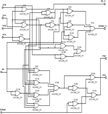
The adder cell designed by Kal and Rajshekhar, 1990 has been redesigned by the N Sharma in 2006 using universal logic gate i.e. NOR gates only which is shown in figure 2.
Figure 2. Logic circuit of Adder Cell using NOR-NOR In figure 3 a modified architecture of the RBSD adder cell has been redesigned by R.K.Saxena in 2010, which is also designed using NOR gates only. As less number of NOR Gates are used and due to decrement in the count of NOR gates propagation delay time is also reduced to get the output.
Figure 3 Logic Circuit of modified Cell using NOR-NOR logic
In 2006, N Sharma proposed the adder cells using universal logic. The logic circuit design using universal gates is highly desirable due to uniformity in the circuit. These circuits can be designed through NAND gates as these gates are in-expensive in manufacturing aspects, therefore they are preferred by the logic designers. Hence the circuit was further redesigned using NAND Gate by N Sharma.
Figure 4 Logic Circuit of RBSD Adder using NAND-NAND Logic
5.Simulation Results:
Logic design of basic RBSD adder cell is designed using Hardware Discriptive Language.This code is then simulated with the help of Modelsim .
Figure.5 Simulation Result of Basic RBSD Adder Cell
Figure.6 Simulation Result of RBSD Adder Cell(NOR-NOR 1 Bit)
Figure.7 Simulation Result of Modified NOR-NOR (1 Bit) Logic RBSD Adder
Figure.8 Simulation Result of NAND-NAND (1 Bit) Logic Adder
6. Comparison:
The timing reports were generated using Xilinx Project Navigator and the comparison chart is shown in figure.
Timing Report for different Adders (ns.)
S.No
No. of Bits
Basic
RBSD
NOR-NOR
RBSD Adder
Modified
NOR-NOR Adder
NAND-NAND
RBSD Adder
1
1
10.56
9.133
7.619
9.142
2
2
10.56
9.133
7.619
9.142
3
4
10.56
9.133
7.619
9.142
4
8
10.56
9.133
7.619
9.142
5
16
10.56
9.133
7.619
9.142
6
32
10.56
9.133
7.619
9.142
7
64
10.56
9.133
7.619
9.142
8
128
10.56
9.133
7.619
9.142
. Table 1: Comparative Analysis
Figure.9 Comparison Chart
7. Conclusion:
In Basic RBSD Adder the simulation delay is constant having the value of 10.569 ns.In NOR-NOR RBSD Adder the simulation delay is also constant but very less than Basic RBSD i.e. 9.133 ns .Further in Modified NOR-NOR RBSD Adder the simulation delay is also constant but very less than NOR-NOR RBSD i.e. 7.619 ns. Next in NAND-NAND RBSD Adder the simulation delay is also constant but greater than Modified NOR-NOR RBSD Adder i.e. 9.142 ns. Hence from this comparison chart we can draw the conclusion that Modified NOR-NOR RBSD Adder is best among all the five signed digit adders.
References:
[1] Avizienis, A., “Signed digit number representation for fast parallel arithmetic”, IRE Trans. Electron Computers., vol EC-10, pp. 389-400, sept.1961. [2] Brent R. P., and Kung H. T., “A Regular Layout for
Parallel Adders”, IEEE Transactions on Computers, vol. C-24, no. 3, pp. 260-264, 1982.
[3] Hallin, T. G. and Flynn M. J., “Pipelining of Arithmetic Functions”, IEEE Transactions of computers, pp. 880-885, 1972.
[4] Neelam Sharma, B. S. Rai and Arun Kumar, “Design of RBSD Adder and Multiplier Circuits for High Speed Arithmetic Operations and Their Timing Analysis”, Special Russian Issue: Advances in computer Science and Engineering, Research in Computing Science23, pp. 243-25, 2006.
[5] Parhami B, “Carry free Addition of Recorded Binary Signed-Digit Numbers”, IEEE Transactions on computers vol. 37 no. 11, pp. 1470-1476 ,1988. [6] Perry D. L., VHDL Programming by Example, Tata
McGraw – Hill Publishing Co. Ltd. Fourth Edition 2003.
[7] Rakesh Kumar Saxena, Neelam Sharma and A. K. wadhwani, “Fast Arithmetic using Signed Digit Numbers and Ternary Logic”, Proceedings of Institute of American Physics, USA, vol. 1146, pp 488-498 July 2009.
[8] Rajashekhar, T.N.and Kal, O., “Fast Multiplier Design using Redundant Signed- Digit Numbers”, International Journal of Electronics vol .69, no. 3, pp –359-368, 1990.
[9] Rajashekhar, T.N. and I-Shi Eric Chen, “A Fast Adder Design Using Signed-Digit Numbers and Ternary Logic”, Proc. IEEE Southern Tier Technical Conference, pp.187-194, Binngamton, New York, April 1990.
[10] Rakesh Kumar Saxena, Neelam Sharma and A. K. Wadhwani “Novel Design of Fast RBSD Adder with Reduced NOR-NOR Logic “International Journal of Computer and Network Security,Vol. 2, No. 7, July \ 2010.