ISSN (Print) : 2320 – 3765 ISSN (Online): 2278 – 8875
I
nternational
J
ournal of
A
dvanced
R
esearch in
E
lectrical,
E
lectronics and
I
nstrumentation
E
ngineering
(A High Impact Factor, Monthly, Peer Reviewed Journal)
Website: www.ijareeie.com
Vol. 7, Issue 2, February 2018
Design and Implementation of Low Power and
High Speed Vedic Multiplier Using 5:2
Compressor
P.Ponsudha1, S.Archana2, S.Keerthana3, E.Shalini4
Assistant Professor, Department of Electronics and Communication Engineering, Velammal Engineering College,
Chennai, Tamilnadu, India1
UG Students, Department of Electronics and Communication Engineering, Velammal Engineering College, Chennai,
Tamilnadu, India2, 3, 4
ABSTRACT: We know that the multiplier unit forms an integral part of processor design.This paper proposes the design of high speed Vedic Multiplier using the compressor which is based on ancient Indian Vedic mathematics that has improved the performance of multiplier. As the technology advent the Multiplier require high speed, low power and small area. In this paper we introduce a new architecture of Vedic multiplier by using 5:2 compressors increasing the speed of Multiplier and reducing the area. It was observed that the parameters like Hardware Complexity, power and Delay are improved. This 5:2 compressor circuit capable of operating at ultra-low voltages. Its power efficacy is derived from the novel design of composite XOR-XNOR gate at transistor level. The new circuit eliminates the weak logic and threshold voltage drop problems, which are the main factors limiting the performance of pass transistor based circuits at low supply voltages. When compared with earlier existing architecture of Vedic multiplier and some common multipliers,The proposed design shows very good results in terms of time delay and area.
I. INTRODUCTION
Multipliers play an important role in today’s digital signal processing and various other applications.In high performance systems such as microprocessor, DSP etc, addition and multiplication of two binary numbers is fundamental and most often used arithmetic operations. Statics shows that more than 70% instructions in microprocessor and most of DSP algorithms perform addition and multiplication[2]. So, these operations dominate the execution time. That’s why, there is need of high speed multiplier. The demand of high speed processing has been increasing as a result of expanding computer and signal processing applications. While using computers and smart phones sometimes we face a situation where the device (hangs) stops responding. One of the reasons behind it is processor speed that motivated us to go for a high speed multiplier design. Low power consumption is also an important issue in multiplier design. To reduce significant power consumption it is good to reduce the number of operation thereby reducing dynamic power which is a major part of total power consumption So the need of high speed and low power multiplier has increased. Designer mainly concentrates on high speed and low power efficient circuit design. The objective of a good multiplier is to provide a physically packed together, high speed and low power consumption unit.
II. RELATED WORKS
ISSN (Print) : 2320 – 3765 ISSN (Online): 2278 – 8875
I
nternational
J
ournal of
A
dvanced
R
esearch in
E
lectrical,
E
lectronics and
I
nstrumentation
E
ngineering
(A High Impact Factor, Monthly, Peer Reviewed Journal)
Website: www.ijareeie.com
Vol. 7, Issue 2, February 2018
III. ADDERS
The various adders are A. Ripple Carry Adder (RCA), B.Carry Look Ahead Adder (CLA), C.Carry Bypass Adder (CBA)
The each and every adder is named based on the propagation of carry between the stages.
A. Ripple Carry Adder:
Logical circuit with multiple full adders can be used for adding N-bit numbers and each full adder inputs a Cin, which is the Cout of the previous adder. Such kind of adder is known as Ripple Carry Adder, since each carry bit "ripples" to the next full adder .The below figure of 4-Bit Ripple Carry Adder. So ripple carry adder in digital electronics is that circuit which produces the arithmetic sum of two binary numbers which can be constructed with full adders connected in cascaded with the carry output from each full adder connected to the carry input of the next full adder in the chain. From which it can be noticed that bits a0and b0 in the figure represent the least significant bits of the numbers which is to be added and sum in form of output represented by the bits s0-s3.[5]
Fig 1: 4 bit ripple carry adder. Fig 2a: Flowchart of CLA
B.Carry Look Ahead Adder:
A carry-Look ahead adder is a fast parallel adder as it reduces the propagation delay by more complex hardware, hence it is costlier. In this design[5], the carry logic over fixed groups of bits of the adder is reduced to two-level logic, which is nothing but a transformation of the ripple carry design. This method makes use of logic gates so as to look at the lower order bits of the augend and addend to see whether a higher order carry is to be generated or not. Carry Look Ahead (CLA) design is based on the principle of looking at lower adder bits of argument and addend if higher orders carry generated. This adder reduces the carry delay by reducing the number of gates through which a carry signal must propagate. As shown in the figure (a), in the generation and propagation stage, the generation values, propagation values are computed. Internal carry generation is calculated in second stage. And in final stage, the sum is calculated
C. Carry Bypass Adder:
In Carry Bypass Adder (CBA), RCA is used to add 4-bits at a time and the carry generated will be propagated to next stage with help of multiplexer using select input as Bypass logic. By pass logic is formed from the productvalues as it is calculated in the CLA. Depending on the carry value and by pass logic, the carry is propagated to the next stage
IV. MULTIPLIERS
ISSN (Print) : 2320 – 3765 ISSN (Online): 2278 – 8875
I
nternational
J
ournal of
A
dvanced
R
esearch in
E
lectrical,
E
lectronics and
I
nstrumentation
E
ngineering
(A High Impact Factor, Monthly, Peer Reviewed Journal)
Website: www.ijareeie.com
Vol. 7, Issue 2, February 2018
involves generation of partial products and their accumulation. The speed of multiplication can be increased by reducing the number of partial products.[2] An efficient multiplier should have following characteristics:-
Fig 2b: Block diagram of CLA. Fig 3: Block diagram of CBA
Accuracy:- A good multiplier should give correct result. Speed:- Multiplier should perform operation at high speed.
Area:- A multiplier should occupies less number of slices and LUTs. Power:- Multiplier should consume less power.
The various types are a. Array Multiplier b. Wallace Tree Multiplier c. Modified Booth Multiplier
A)Array Multiplier:
ISSN (Print) : 2320 – 3765 ISSN (Online): 2278 – 8875
I
nternational
J
ournal of
A
dvanced
R
esearch in
E
lectrical,
E
lectronics and
I
nstrumentation
E
ngineering
(A High Impact Factor, Monthly, Peer Reviewed Journal)
Website: www.ijareeie.com
Vol. 7, Issue 2, February 2018
Fig 4: Simplified diagram of 32 bit Array multiplier.
B)Wallace Tree Multiplier:
Fig 5: Structure of Wallace Tree Multiplier. Fig 6: Modified Booth Algorithm Realization.
C)Modified Booth Multiplier:
The modified Booth encoding (MBE), or modified Booth’s algorithm. The recoding method is widely used to generate the partial products for implementation of large parallel multipliers, which adopts the parallel encoding scheme. The original version of Booth algorithm (Radix-2) had two drawbacks: The number of add subtract operations and the number of shift operations becomes variable and becomes inconvenient in designing parallel multipliers. The algorithm becomes inefficient when there are isolated 1‟s. These problems can be overcome by modified Booth algorithm. MBA
ISSN (Print) : 2320 – 3765 ISSN (Online): 2278 – 8875
I
nternational
J
ournal of
A
dvanced
R
esearch in
E
lectrical,
E
lectronics and
I
nstrumentation
E
ngineering
(A High Impact Factor, Monthly, Peer Reviewed Journal)
Website: www.ijareeie.com
Vol. 7, Issue 2, February 2018
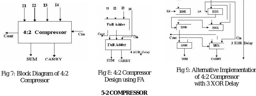
V. PROPOSED 4:2 AND 5-2 COMPRESSOR DESIGNS 4-2 COMPRESSOR
The 4:2 compressor structure actually compresses five partial products bits into three [1,2,3]. The architecture is connected in such a way that four of the inputs are coming from the same bit position of the weight j while one bit is fed from the neighboring position j-1(known as carry-in)[7]. The outputs of 4:2 compressor consists of one bit in the position j and two bits in the position j+1.This structure is called compressor since it compresses four partial products into two(while using one bit laterally connected between adjacent 4:2 compressors). Figure 1 shows the block diagram of 4-2 compressor. A 4-2 compressor can also be built using 3-2 compressors. It consists of two 3-2 compressors (full adders) in series and involves a critical path of 4 XOR delays as shown in Figure 2. An alternative implementation is shown in Figure 3. This implementation is better and involves a critical path delay of three XOR's , hence reducing the critical path delay by 1 XOR. The output Cout, being independent of the input Cin accelerates the carry save summation of the partial products as proposed in [3].
5-2 COMPRESSOR
The block diagram of a (5:2) compressor shown below has seven inputs and four outputs. Five of the inputs are the primary inputs I1, I2, I3,I4 and I5 and two other inputs, Cinl and Cin2 . The architecture is connected in such a way that five of the inputs come from the same bit position of the weight j while other two inputs (Cinl and Cin2) are fed from the neighboring position j-1(known as carry-in). The outputs of 5:2 compressor consists of one bit in the position j (sum) and two bits in the position j+1 (cout1, cout2, carry). A simple implementation of the (5,2) compressor is to cascade three (3,2) full adders in a hierarchical structure, as shown. This architecture has a critical path delay of 6 XOR gates. Figure below shows another architecture of a (5:2 ) compressor. The implementation shows that this design has a critical path delay of 4XOR + 1MUX unlike the conventional implementation with a delay of 5XOR[7].
Fig 7: Block Diagram of 4:2
Compressor
Fig 8: 4:2 Compressor Design using FA
Fig 9: Alternative Implementation
of 4:2 Compressor with 3 XOR Delay
Fig 10: 5:2 Compressor using Full Adders
Fig 11. Alternative Implementation of 5:2 Compressor
ISSN (Print) : 2320 – 3765 ISSN (Online): 2278 – 8875
I
nternational
J
ournal of
A
dvanced
R
esearch in
E
lectrical,
E
lectronics and
I
nstrumentation
E
ngineering
(A High Impact Factor, Monthly, Peer Reviewed Journal)
Website: www.ijareeie.com
Vol. 7, Issue 2, February 2018
In order to further optimize the design of the existing 4-2 and 5-2 compressor shown, the authors propose the optimized transistor implementation of the above mentioned compressors. In the proposed compressor design, the XOR gate and MUX designs are appropriately replaced with minimum transistor implementation to design the circuit such that it has no direct supply from VDD. The optimal small area, low power, high throughput XOR design was proposed. The XOR design proposed has no power supply and is referred as Powerless XOR. Moreover , the MUX employed in the design can be implemented with 2 transistors as mentioned[7]. Thus, it can be inferred that the proposed 4:2 compressor design is an optimized version as the authors have optimesed the entire design starting from the basic cell level. Thus, the 4-2 and 5-2 compressors are implemented with bare minimum of 20 and 30 transistors respectively.
VI.VEDIC MULTIPLIER
Multiplication is one of the important arithmetic operation in signal processing applications. Signal processing involves multiplication, speed and accuracy is the main constraint in the multiplication process. Speed can be achieved by reducing the computation process in the multiplication technique. Vedic multiplier is efficient multiplication technique. The efficient Vedic multiplication technique is used. The 8-bit Vedic multiplier is designed by using four 4x4 Vedic multiplier and square root carry select adder (SQRT-CSLA).
Tab:I Comparison of Area between booth, Modified booth and Vedic multiplier
Parameters
Booth
Modified Booth
Vedic No.of LUTs
31 % 20 % 12 % No.Of Slices
35 % 27 % 10 %
Fig 13: Simulation result of Vedic Multiplier Fig 14: Synthesis of Vedic Multiplier
ISSN (Print) : 2320 – 3765 ISSN (Online): 2278 – 8875
I
nternational
J
ournal of
A
dvanced
R
esearch in
E
lectrical,
E
lectronics and
I
nstrumentation
E
ngineering
(A High Impact Factor, Monthly, Peer Reviewed Journal)
Website: www.ijareeie.com
Vol. 7, Issue 2, February 2018
Tab:II Comparison of time and power between booth, Modified booth and Vedic multiplier
Parameters
Booth
Modified Booth
Vedic
TIME 52.627 ns 31.929 ns 19.959ns
POWER 135 mw 133 mw 85 mw
VII. CONCLUSION
Multiplier in special application processors like Digital Signal Processor (DSPs) improves the speed of operation since the entire signal and data processing operations involve multiplication. Multiplication plays a vital role in DSP applications (like DFT, convolution, FFT etc.), Arithmetic and logic unit (ALU), and multiply and Accumulate (MAC) unit. High Speed Multiplication thus becomes a necessity to increase the performance of processor. This paper presents a technique to modify the architecture of the Vedic (UrdhvaTiryakbhyam)multiplier by using compressor in order to reduce area and delay to improve overall performance. The proposed (5:2) compressor has been designed with special consideration on output drivability to ensure that it can function reliably at low voltages when these cells are employed in the tree structured multiplier and multiplyaccumulator. Simulation results show that the proposed (5:2) compressor is able to function at supply voltage as low as 0.7V. These designs have the principle advantage that in addition to reduced transition activity, they have no direct connections to the power-supply and is totally driven by the input signals, leading to a noticeable reduction in short-circuit power consumption.
REFERENCES
[1]Yogendri,Anil Kumar Gupta,”Design of high performance 8-bit Vedic multiplier” published in Advances in Computing, Communication, & Automation (ICACCA) by IEEE.
[2]S.Alexander,”A Review of Different Multipliers in Digital Circuits”inInternational Journal of MC Square Scientific Research Vol.4, No.1 Nov 2012
[3] Manish Kumar and JonaliNath, “Design of an Energy Efficient 4-2 Compressor”cited in the article: 2017 IOP Conf. Ser.: Mater. Sci. Eng. 225
012136
[4] IEEE paper on “Dual-Quality 4:2 Compressors for Utilizing in Dynamic Accuracy Configurable Multipliers” by OmidAkbari, Mehdi Kamal, Ali Afzali-Kusha, and MassoudPedram
[5] Jasbir Kaur, LalitSood,”Comparison Between Various Types of Adder Topologies”- March 2015.
[6] Soniya, Suresh Kumar, “A Review of Different Type of Multipliers and Multiplier-Accumulator Unit.” In International Journal of Emerging Trends & Technology in Computer Science (IJETTCS)
[7]Pallavi Devi Gopineedi, HimanshuThapliyal, M.B Srinivas and Hamid R. Arabnia,”Novel and Efficient 4:2 and 5:2 Compressors with Minimum number of Transistors Designed for Low-Power Operations”
[8] A. Weinberger and J. L. Smith, “A logic for high speed addition”, National Bureau of Standards, Circulation 591, pp. 3-12, 1958. [9] T. Lynch and E. Swartzlander, “A spanning tree carry look ahead adder”, IEEE Trans. on Computers, vol. 41, no. 8, pp. 931-939, 1992. [10]G. Yang, S. Jung, K. Baek, S. Kim, S. Kim, S. Kang, “A 32-bit carry lookahead adder using dual-path all-N logic”, IEEE Trans. on VLSI Systems, vol. 13, no. 8, pp. 992-996, 2005.
[11] S. Hauck, M. Hosler and T. Fry, “High performance carry chains for FPGAs”, IEEE Trans. on VLSI Systems, vol. 8, no. 2, pp. 138-147, 2000. [12]C. Huang, J. Wang, C. Yeh and C. Fang, “The CMOS carry-forward adders”, IEEE Journal of Solid-State Circuits, vol. 39, no. 2, pp. 327- 336, 2004.