Meta Paged Flash Translation Layer
Shinde Pratibha PG Student, Dept.of Info.Tech.
PDVVP COE, Ahmednagar, Pune University.
Srinivas
Asst Prof, Dept. of Info .Tech. RM COE,
Hyderabad, JNT University.
Abstract -- Today NAND Flash Memory is used in handheld electronic devices like mobile, cameras, iPODS, music players, is also used as an alternative storage medium for Hard Disk Drives (HDD) in PCs and Labtops. Though Flash has a faster access and is a good alternative storage media for HDD. NAND flash memory has many advantageous features as a storage medium, such as superior performance, shock resistance, and low power consumption. However, the erase-before-write nature and the limited number of write/erase cycles are obstacles to the promising future of NAND flash memory. An intermediate software layer called Flash Translation Layer (FTL) is used to overcome these obstacles. Various trade offs arises in the design of FTLs, depending upon the various address mapping schemes used for logical to physical address translation. Various researchers have invented different FTL design to optimize the performance while achieving the objectives and goals. This paper takes a review of all these FTL schemes and presents an innovative idea to improve the performance of the FTL presented earlier.
1. INTRODUCTION
Flash memory which is an electronic non volatile memory can be electrically erased and reprogrammed. It was developed from EEPROM (electrically erasable programmable read-only memory). While a flash device can read any of its pages, it may only write to one that is in a special state called erased. This is called as ‘erase before update’ characteristics of Flash. Due to which flash do not support overwrite i.e. in-place update operation, instead it supports out of-place-update.
Flash Translation Layer maintains a mapping table of virtual address to physical address.
It has efficient space for storing mapping tables. Mapping tables are stored in SRAM .It has the lowest overhead for: Garbage collection and Address translation i.e. requires minimum number of valid page read, and page writes required during garbage collection and address translation. The granularity of mapping unit (e.g. page or block or hybrid) that the mapping scheme uses for address translation that affects the performance of any FTL. These schemes are described in next section.
Figure 1 : Interface of Flash storage to host system 2. REVIEW OF PREVIOUS FTL SCHEMES A. Page Level Mapping:
In page mapping scheme the smallest logical unit that FTL uses for address translation is a page. A page is made up of certain number of smallest units called as sector. This is most efficient scheme in that a logical page can be mapped into any physical page in flash memory. This mapping information is kept in the form of tables called as mapping tables.
B. Block Level Mapping:
In block mapping scheme, the smallest logical unit, used by FTL for address translation, is a block. A block is also smallest erase unit for flash memory. In order to reduce the map table size, block mapping can be utilized. In block mapping the logical page address is divided into a logical block number and a page offset. For block mapping scheme the block map table consists of entries storing the physical block number of the corresponding logical blocks.
C. Hybrid Level Mapping:
It combines Page Level Mapping schemes and Block Level Mapping schemes .Physical blocks are logically partitioned into two groups :Data Blocks & Log Blocks. 1) BAST (Block Associative Sector Translation)
It consists of two types of blocks: data blocks mapped by block mapping and log block that act as update buffer, mapped by page mapping.
RAM requirement of BAST is also less . Only the page tables of log blocks are to be maintained in RAM and log blocks are very few in number hence RAM space for keeping mapping information is less.
2) Super Block scheme:
Attempts to exploit the block level spatial locality . It maintains page level mapping by separating hot and cold data within a superblock and consequently the garbage collection efficiency is achieved. However, this approach uses a three-level address translation mechanism .Superblock consists of a set of adjacent logical blocks. To reduce extra storage and flash memory operations ,the mapping information is stored in the spare area of NAND flash memory.
3) FAST (Fully Associative Sector Translation):
FAST is known as optimal hybrid FTL in efficiency and performance . All the data blocks are mapped using block mapping scheme. Log blocks are mapped using page mapping. The scheme uses two types of log blocks: A log block for sequential writes and a small number of log blocks for random writes.
If data are overwritten in sequential write and are stored in a sequential. Log blocks to be shared by all data blocks. This improves the utilization of log blocks as compared to BAST. Both type of log blocks are shared by all the data blocks and data from a single data block can scatter over many log blocks. Hence, name fully associative. FAST keeps the single sequential log block dedicated for sequential writes and random writes. Lookup complexity of FAST is much larger than BAST, as in this scheme the data structures maintaining the mapping information are not simple, due to associativity of data and log blocks. Therefore for doing a lookup operation all the log blocks need to be searched because in the mapping table the index does not indicate the logical page number, but instead it indicates the physical page number and the value stored at that index entry indicate the logical page number. Hence for lookup of a logical page number linear search is performed, a time consuming operation. For example if the capacity of the storage flash under consideration is 4GB, the block size is 128KB, the page size is 2KB, and the number of log blocks is 320. The RAM requirement is less and is same as that of the BAST scheme.
4) LAST (Locality-Aware Sector Translation):
providing multiple sequential log blocks to exploit spatial locality in workloads. It further separates random log blocks into hot and cold regions to reduce full merge cost . LAST depends on an external locality detection mechanism to provide dynamic separation. The fixed size of the sequential log buffer brings about the overall garbage collection overhead.
5) AFTL (Adaptive Two-Level Flash Translation Layer) : Tto maintain the advantages of the fine-grained and coarse- grained address translation mechanisms. AFTL provides a block-device emulation of flash memory .That is, coarse-fine switches incur corresponding fine to-coarse switches, which causes overhead in valid data page copies. Additionally, only if all of the data in its primary block appear in the replacement block, both corresponding coarse-grained slot and its primary block can be removed. 6) DFTL Scheme:
DFTL maintains two types of tables in SRAM, namely, Cached Mapping Table (CMT) and Global Translation Directory (GTD). CMT stores a small number of page mapping information like a cache for a fast address translation in SRAM. It achieves high block utilization also it completely remove full merge operations this is the advantage. DFTL suffers from frequent updates of translation pages in case of write dominant access patterns or garbage collection this is the disadvantage. DFTL achieves a good write performance but cannot achieve as good read performance as hybrid FTLs under read dominant workloads due to its intrinsic two-tier address translation overhead. This scheme is paradigm shift from the previous hybrid mapping schemes. It is fundamentally a page mapping scheme. It maintains the complete page map table in the flash memory itself. Hence its RAM requirement is much less the other schemes.
3. PROPOSED WORK:
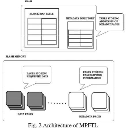
Fig. 2 Architecture of MPFTL The terms related to Terminology
A. Sector
Is the smallest amount of data which is read or written at a time. That is, sector is unit of a read, write operation in flash.
B. Address translation
Is conversion of logical address that is received by flash from file system into physical address i.e. the actual physical on flash address where the data actually resides. C. Mapping table
Data structure used to store all logical to corresponding physical address.
Uses a special address translation mechanism that does with the constrained size of SRAM
D. Features
It is basically page level mapping. Uses a special address translation mechanism that does with the constrained size of SRAM. It overcomes the limitation of limited SRAM size of controller for storing mapping information, as it maintains the map table on flash itself.
E. Scope
NAND Flash is used as portable storage medium for computers, digital cameras, cell phones and other devices. flash memory is widely used in:
Notebook computers Personal computers Digital cameras Cell phones Music players MP3 players
Television set-top boxes Security systems Military systems F. Goals
To develop a mapping scheme for FTL that gives the benefit of page level mapping for any general workload of read or write. Overcome the page level mapping limitation of limited Controller’s SRAM. To reduce the number of erase operations required for garbage collection. To reduce the address translation overhead.
G. Objectives
To develop basically a page mapping scheme for FTL which will store the entire page map table in the flash itself. To develop basically a page mapping scheme for FTL which will store the entire page map table in the flash itself. H. Constrain
In case of a full read load, the performance of this mapping may degrade little bit over the FAST system.
4. RESEARCH METHODOLOGY A: Steps to acquire input:
The input to the project is disk I/O workload. For this a realistic characteristics representative workloads is collected. Various tool, for e.g. Diskmon tool are available to collect I/O workloads. The trace files for various categories of workload are available on the website of Storage Performance Council SPC.Characteristics of the representative workloads are analyzed by SPC. To accomplish this, the individual I/O commands issued by the host processor(s) are collected and analyzed in order to create a list of the I/O parameters.
B. Steps To Interpret The Input :
The input trace is having variable length records separated by comma (hex 2C), with each record being terminated by a newline character (\n). This record is divided into five fields.
Each input record consists of five values which indicate 5 different input parameters. All these five fields in a record collectively describe a single disk IO request. This I/O request is taken as input I/O request for the simulated flash. The five parameters are:
Field 1: Application specific unit (ASU)
The ASU is a positive integer representing the application specific unit. . For example if device under consideration is hard disk drive then this denotes the logical volume number. If there are a total of n units described in the complete trace file, then the trace file must contain at least one record for each of units 0 through n-1.
Field 2: Logical block address (LBA)
The LBA field is a positive integer that describes the ASU block offset of the data transfer for this record. where the size of a block is contained in the description of the trace file. This offset is zero based, and may range from 0 to n-1, where n is the capacity in blocks of the ASU.
Field 3: Size
The size field is a positive integer that describes the number of bytes transferred for this record.
There is no upper limit on this field, other than the restriction that sum of the address and size fields must be less than or equal to the capacity of the ASU.
Field 4: Opcode
The opcode field is a single, case insensitive character that defines the direction of the transfer. There are two possible values for this field: “R” (or “r”) indicates a read operation. This implies data transfer from the ASU to the host computer.
Field 5: Timestamp
The timestamp field is a positive real number representing the offset in seconds for this I/O from the start of the trace. The format of this field is “s.d” where “s” represents the integer portion, and “d” represents the fractional portion of the timestamp.
Field 6 (through n): Optional field(s):
Optional fields may be added to the each record in the trace file by the simple expedient of inserting a field separator (comma), followed by the field. If there is more than one field to be added, then each field must be separated from the preceding field by the comma field separator.
5. DATABASE DESIGN
Database is in the form of trace file. In order to create a list of the I/O parameters associated with a specific benchmark, the characteristics of the representative workloads should be analyzed and well understood.
The individual I/O commands issued by the host processor(s) are collected and analyzed. Since many different analysis programs may be used, and these programs will in all probability be run “after the fact”, a goal of the SPC is to collect I/O trace data from various systems. The trace file is composed of variable length ACSII records, rather than binary data. This format is somewhat wasteful of storage space and places higher CPU demands on analysis programs, it offers many advantages from a legibility and portability standpoint. Each record in the trace file represents one I/O command, and consists of several fields. The following is an example of the first few record of a trace file:
0,20941264,8192,W,0.551706,Alpha/NT 0,20939840,8192,W,0.554041
The individual fields are separated by a comma with the trace record being terminated by a newline character (\n). There is no special end-of-file delimiter; that function being left to the individual operating systems.
6. IMPLEMENTATION
The project is implemented using an SSD simulator. This simulator is designed object oriented language and can be integrated with any FTL designed by the testers. Initially the project will create an SSD object, which will process the read and write requests. These read and write requests provided to the SSD are in the form of a text file called as trace file, whose format is described in earlier section. The SSD object requires a controller which. A controller uses an FTL. This FTL used will be the FTL designed by the simulator.
7. EXPERIMENTAL SETUP
For experimental result simulation of a 32GB NAND flash memory with configurations shown in table below is done.
TABLE I
FLASH MEMORY CONFIGURATION
Input Parameters values
Page read to register 25µ
Page write from register 200µ
Block Erase 1.5ms
Serial Access to register data 50µ
Page Size 4KB
Data register size 2KB
Block size 256KB
To test all the cases of workloads various types of workloads are selected as shown in table below.
Websearch3 and financial1 and financial2 traces are made by Storage Performance Council (SPC). Websearch3 is a good read intensive I/O trace.
TABLE 2 TYPES OF WORKLOADS
Workloads Request Ratio (Read: Write)
Inter-arrival Time(avg)
Websearch 3 R.99% W: 1% 70 ms Financial 1 R.: 22% W: 78% 8 ms Financial 2 R: 82% W: 18% 11ms Random_read R: 99% W: 1% 11 ms Random _write R: 10% W: 90% 11ms
Financial1 shows a good write intensive workload and is collected from an OLTP application running at a financial institution.
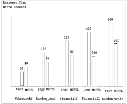
8. CONCLUSION
Proposed idea i.e. Meta Paged Flash Translation Layer (MPFTL) is page level mapping scheme and avoids recursive merge and full merge required during garbage collection . It achieves high block utilization and hence improves overall performance.
From the response time got from the various workload it is observed that the proposed innovative algorithm outperforms the FAST scheme. FAST is taken as a representative scheme for comparison as it is has been considered an optimal one among the various FTL schemes that are available. The merge operation required during garbage collection specially in random write workload is eliminated and the random write performance is improved very much in case of the proposed scheme i.e. Mata Paged FTL (MPFTL). However in case of sequential read the MPFTL does not outweighs the FAST scheme but gives a comparative performance with FAST i.e. in case of the workload websearch3 both the schemes have near about same performance.
The future scope of this project is improve better data structure for managing the page table, so that the look time for the page search operation is improved.
REFERENCES
[1] A. Gupta, Y. Kim, and B. Urgaonkar, “DFTL: a Flash Translation Layer Employing Demand-based Selective Caching of Page-level Address Mappings,” in ASPLOS, 2009.
[2] Hsin Hung Lin, “An Adaptive Flash Translation Layer for High-Performance Storage Systems” IEEE Transactions on page: 953 – 965, June 2010, ISSN: 02780070, Volume: 29
[3] Liu D., Wang Y., Qin Z., Shao Z., Guan Y.: A Space Reuse Strategyfor Flash Translation Layers in SLC NAND Flash Memory Storage Systems, IEEE Transactions on Very Large Scale
Integration (VLSI) Systems, pages 1-14, May – 2011, ISSN: 1063-8210 Volume: PP Issue:99
[4] Shin I.: Light weight sector mapping scheme for NAND-based block devices, IEEE Transactions on Consumer Electronics, pages: 651 – 656, May 2010, ISSN: 0098-3063 Volume: 56 Issue:2
[5] S. Lee, D. Shin, Y. Kim, and J. Kim. LAST: Locality-Aware Sector Translation for NAND Flash Memory-Based Storage Systems. In Proceedings of the International Workshop on Storage and I/O Virtualization, Performance, Energy, Evaluation and Dependability (SPEED2008), Feburary 2008.
[6] “FlashSim: A Simulator for NAND Flash-Based Solid-State Drives” in Advances in System Simulation, 2009. SIMUL '09. First International Conference on pages 125-131 ISBN: 978-1-4244- 4863-0
[7] J. Kang, H. Jo, J. Kim, and J. Lee. A Superblock-based FlashTranslation Layer for NAND Flash Memory. InProceedings of the International Conference on Embedded Software (EM-SOFT) , pages 161–170, October 2006. ISBN 1-59593-542-8.
[8] S. Lee, D. Park, T. Chung, D. Lee, S . Park, and H. Song. A Log Buffer based FlashTranslation Layer Using Fully Associative Sector Translation. IEEE Transactions on Embedded Computing Systems, 6(3):18, 2007. ISSN 1539–9087.
[9] T.-S. Chung, D.-J. Park, S. Park, D.-H. Lee, S.-W. Lee, and H.-J. Song, “A survey of Flash Translation Layer,” J. Syst. Archit., vol. 55, no. 5-6, 2009.
[10] UMass, “Websearch Trace from UMass Trace Repository,” http://traces.cs.umass.edu/index.php/Storage/Storage, 2002.