Scholarship at UWindsor
Scholarship at UWindsor
Electronic Theses and Dissertations Theses, Dissertations, and Major Papers
2017
In-Memory Computing by Using Nano-ionic Memristive Devices
In-Memory Computing by Using Nano-ionic Memristive Devices
Amirali Amirsoleimani University of Windsor
Follow this and additional works at: https://scholar.uwindsor.ca/etd
Recommended Citation Recommended Citation
Amirsoleimani, Amirali, "In-Memory Computing by Using Nano-ionic Memristive Devices" (2017). Electronic Theses and Dissertations. 7346.
https://scholar.uwindsor.ca/etd/7346
Memristive Devices
by
Amirali Amirsoleimani
A Dissertation
Submitted to the Faculty of Graduate Studies through the
Department of Electrical and Computer Engineering in Partial Fulfillment
of the Requirements for the Degree of Doctor of Philosophy at the
University of Windsor
All Rights Reserved. No Part of this document may be reproduced, stored or otherwise
retained in a retreival system or transmitted in any form, on any medium by any means
by
Amirali Amirsoleimani
APPROVED BY:
M. Sachdev, External Examiner
Department of Electrical and Computer Engineering, University of Waterloo
A. Jaekel
School of Computer Science
M. Khalid
Department of Electrical and Computer Engineering
M. Mirhassani
Department of Electrical and Computer Engineering
M. Ahmadi, Advisor
Department of Electrical and Computer Engineering
Publication
I am aware of the University of Windsor Senate Policy on Authorship to add the following
and I certify that I have properly acknowledged the contribution of other researchers to
my thesis and have obtained written permission from each co-author to include the above
material in my document. I hereby declare that this thesis incorporates material that is
result of joint research and includes 6 original papers that have been previously published,
as follows:
Thesis Chapter Publication Title Publication status
Chapter 2 Accurate Charge Transport Model for Nanoionic Memristive Devices, in
Microelectronics Journal Published
Chapter 3
Brain-inspired Pattern Classification with Memristive Neural Network Using the Hodgkin-Huxley Neuron, in Proceedings of the 23rd IEEE International
Conference on Circuits and Systems (ICECS)
Published
Chapter 4
STDP-based Unsupervised Learning of Memristive Spiking Neural Network by Morris-Lecar Model, in 2017 International Joint Conference on Neural
Network (IJCNN) (Best Poster Honorable Mention Award)
Published
Chapter 5 A Memristive CVNS Analog Adder, in 2017 IEEE European Conference on
Circuit Theory and Design (ECCTD) Published
Chapter 6 4:2 compressor cells design with nanoionic memristive devices, in 2016 IEEE
International Symposium on Circuits and Systems (ISCAS) Published
Chapter 7 Logic design on mirrored memristive crossbars, in IEEE Transactions on
Circuits and Systems II: Express briefs Published
Chapter 2 of this thesis was co-authored with Jafar Shamsi, Majid Ahmadi, Arash
Yakop-cic, Omid Kavehei and Said Al-Sarawi. In all cases, the key ideas, primary contributions,
data analysis and writing were performed by the author, and the contribution of co-authors
was providing the modeling for the state of art and extracting the data from the
fabri-cated device. Chapter 3 was co-authored with Majid Ahmadi, Arash Ahmadi and Mounir
Boukadoum. In all cases, the key ideas, primary contributions, simulations and data
analy-sis were done by the author and the contribution of co-authors was on providing feedback
on refinement of ideas and editing the manuscript. Chapter 4 was co-authored with Majid
Ahmadi and Arash Ahmadi. In all cases, the key ideas, primary contributions, simulations
and data analysis were done by the author and the contribution of co-authors was on
provid-ing feedback on refinement of ideas and editprovid-ing the manuscript. Chapter 5 was co-authored
with Majid Ahmadi and Arash Ahmadi. In all cases, the key ideas, primary contributions,
simulations and data analysis were done by the author and the contribution of co-authors
was on providing feedback on refinement of ideas and editing the manuscript. Chapter 6
was co-authored with Mehri teimoori, Majid Ahmadi and Arash Ahmadi. In all cases, the
key ideas, primary contributions, simulations and data analysis were done by the author
and the contribution of co-authors was on providing feedback on refinement of ideas and
editing the manuscript. Chapter 7 was co-authored with Majid Ahmadi and Arash Ahmadi.
In all cases, the key ideas, primary contributions, simulations and data analysis were done
by the author and the contribution of co-authors was on providing feedback on refinement
of ideas and editing the manuscript.
I certify that I have obtained a written permission from the copyright owner(s) to include
the above published material(s) in my thesis. I certify that the above material describes
work completed during my registration as graduate student at the University of Windsor.
I am aware of the University of Windsor Senate Policy on Authorship and I certify that
I have properly acknowledged the contribution of other researchers to my thesis. I certify
that, with the above qualification, this thesis, and the research to which it refers, is the
I declare that, to the best of my knowledge, my thesis does not infringe upon anyones
copyright nor violate any proprietary rights and that any ideas, techniques, quotations, or
any other material from the work of other people included in my thesis, published or
oth-erwise, are fully acknowledged in accordance with the standard referencing practices.
Fur-thermore, to the extent that I have included copyrighted material that surpasses the bounds
of fair dealing within the meaning of the Canada Copyright Act, I certify that I have
ob-tained a written permission from the copyright owner(s) to include such material(s) in my
thesis. I declare that this is a true copy of my thesis, including any final revisions, as
ap-proved by my thesis committee and the Graduate Studies office, and that this thesis has not
By reaching to the CMOS scaling limitation based on the Moore’s law and due to the
increasing disparity between the processing units and memory performance, the quest is
continued to find a suitable alternative to replace the conventional technology. The recently
discovered two terminal element, memristor, is believed to be one of the most promising
candidates for future very large scale integrated systems.
This thesis is comprised of two main parts, (Part I) modeling the memristor devices,
and (Part II) memristive computing. The first part is presented in one chapter and the
second part of the thesis contains five chapters. The basics and fundamentals regarding
the memristor functionality and memristive computing are presented in the introduction
chapter. A brief detail of these two main parts is as follows:
• Part I: Modeling-This part presents an accurate model based on the charge
trans-port mechanisms for nanoionic memristor devices. The main current mechanism
in metal/insulator/metal (MIM) structures are assessed, a physic-based model is
pro-posed and a SPICE model is presented and tested for four different fabricated devices.
An accuracy comparison is done for various models for Ag/TiO2/ITO fabricated
de-vice. Also, the functionality of the model is tested for various input signals.
• Part II: Memristive computing-Memristive computing is about utilizing memristor
to perform computational tasks. This part of the thesis is divided into neuromorphic,
– Neuromorphic computing- Two chapters of this thesis are about
biological-inspired memristive neural networks using STDP-based learning mechanism.
The memristive implementation of two well-known spiking neuron models,
Hudgkin-Huxley and Morris-Lecar, are assessed and utilized in the proposed
memristive network. The synaptic connections are also memristor devices in
this design. Unsupervised pattern classification tasks are done to ensure the
right functionality of the system.
– Analog computing-Memristor has analog memory property as it can be
pro-grammed to different memristance values. A novel memristive analog adder is
designed by Continuous Valued Number System (CVNS) scheme and its circuit
is comprised of addition and modulo blocks. The proposed analog adder design
is explained and its functionality is tested for various numbers. It is shown that
the CVNS scheme is compatible with memristive design and the environment
resolution can be adjusted by the memristance ratio of the memristor devices.
– Digital computing-Two chapters are dedicated for digital computing. In the
first one, a development over IMPLY-based logic with memristor is provided to
implement a 4:2 compressor circuit. In the following chapter, A novel
resistive-type, single-step and multiple fanin and fanout memristive logic is designed
over a novel mirrored memristive crossbar platform. Different logic gates are
designed with the proposed memristive logic method and the simulations are
provided with Cadence to prove the functionality of the logic. The logic
This thesis is the outcome of the 3 years research in department of electrical and computer
engineering, University of Windsor. To the best of my knowledge, this is the first Ph.D.
thesis on emerging topic of memristive systems in Canada and it has been a great privilege
to be the first Ph.D. student on this topic in the region. I gratefully acknowledge the people
who assisted me along this path.
First and foremost I would like to express my gratitude and appreciation to Dr. Majid
Ahmadi, my supervisor for his invaluable guidance and constant support throughout
differ-ent stages of this work. He has been a great infludiffer-ential mdiffer-entor in my scidiffer-entific career while
he means like a father for me and his guidance helped me in all the time of research and
writing of this thesis. I could not have imagined having a better advisor and mentor for my
Ph.D study. He has certainly shaped me as a researcher and has led me where I am now.
Another key person whom I strongly indebted to is Dr. Arash Ahmadi. I had this
chance again to work closely with my previous M.Sc. advisor who always inspired me
with his beautiful mind and unconventional thinking method which most of the time turns
impossible to possible. His way of thinking inspires me to approach problem in different
ways. I appreciate all his contribution, time, ideas and the direction he provided for me.
My gratitude also goes to Dr. Said Al-Sarawi for his kind assistance and review of the
modeling section. Mr. Jafar Shamsi, Dr. Chris Yakopcic, Dr. Mostafa Rahimi Azghadi,
Dr. Omid Kavehei, Mr. Hamid Soleimani, Mr. Mohammad Bavandpour and Ms. Mehri
In addition, I would like to thank the rest of my thesis committee, Dr. Mitra Mirhassani,
Dr. Mohammed Khalid and Dr. Arunita Jaekel for their participation in my seminars, their
constructive comments and advice. I would also like to include my gratitude to Ms. Andria
Ballo and Mr. Frank Cicello for their kind support and continuous help during my time
as a graduate student. I wish to express my warm and sincere thanks to Dr. Esam
Abdel-Raheem for his kind support.
My sincere thanks also goes to Dr. Rashid Rashidzadeh, who provided me an
opportu-nity to join his industrial team as an intern, and who gave me the access to the laboratory
and research facilities. Also, I appreciate his assistance and productive comments for
ana-log implementation problems.
I would also like to thank my friends and colleagues in the University of Windsor
whom have supported and believed in me: Behrouz Chegeni, Shaghayegh Gomar, Ali
Dianat, Mohammad Anvaripour, Mojtaba Kordestani, Parham Hosseinzadeh Namin, Bahar
Yousefi, Abubakr Sasi, Dr. Luay Taha, Iman Taha and Dr. Faruq Awin.
My endless appreciation goes to my family, my mother, my father, my brother and
my sister, who always supported me regardless of the situation in any condition and always
endow me with infinite love, encouragement and patience. I also want to express my sincere
thanks to my grand mother and grand father whom I wish his soul will rest in peace for their
unconditional love and support. In addition, I like to thank my mother in law and my father
in law for their support and patience.
Last but not least, the warmest thank goes to my dear wife,Saeideh, who always stayed
by me shoulder to shoulder during this long journey. I dedicated this thesis to her by all my
Declaration of Co-Authorship/Previous Publication iv
Abstract vii
Acknowledgments ix
List of Figures xv
List of Tables xxiv
List of Abbreviations xxvi
1 Introduction 1
1.1 Definition of Memristor . . . 2
1.2 Memristor Modeling . . . 5
1.3 Memristor Crossbar . . . 15
1.4 Applications of Memristor . . . 18
1.4.1 Memory . . . 19
1.4.2 Logic . . . 20
1.4.3 Neuromorphic . . . 22
1.5 Outline of Thesis . . . 22
References 27
2 Accurate Charge Transport Model for Nanoionic Memristive Devices 33
2.1 Introduction . . . 33
2.2 Memristor Device Functionality . . . 35
2.3 Review of Memristor Models . . . 36
2.4 Memristor Charge Transport Mechanisms . . . 39
2.4.1 Tunneling Current . . . 42
2.4.2 Thermionic Current . . . 44
2.4.3 Ohmic Current . . . 44
2.5 An Accurate SPICE-Based Memristor Model . . . 45
2.6 Memristor Model With Charge Transport Mechanisms (CTM) Analysis . . 54
2.7 Conclusion . . . 58
References 60 3 Brain-inspired Memristive Neural Network Using Hodgkin-Huxley Neuron 64 3.1 Introduction . . . 64
3.2 Hudgkin Huxley Neuron . . . 66
3.3 STDP Learning Mechanism with Memristor Synapses . . . 70
3.4 Proposed SNN Architecture and Behaviour . . . 71
3.5 Pattern Classification Results . . . 73
3.5.1 2×2 Proposed SNN . . . 73
3.5.2 4×2 Proposed SNN . . . 75
3.6 Conclusion . . . 75
4.2 Memristor Device and Its Functionality . . . 83
4.3 Morris-Lecar Neuron . . . 84
4.4 STDP Learning Mechanism with Memristor Synapses . . . 89
4.5 The Memristive SNN with ML Neuron . . . 90
4.6 Pattern Classification Results . . . 93
4.7 Conclusion . . . 96
References 98 5 A Novel CVNS Adder with Memristive Analog Memory 100 5.1 Introduction . . . 101
5.2 Continuous Valued Number System (CVNS) . . . 102
5.3 Memristor Device and Its Programming . . . 104
5.4 Memristive Continuous Valued Number System (MCVNS) Adder . . . 106
5.4.1 Memristive Addition Configuration . . . 106
5.4.2 Memristive Modulo Configuration . . . 108
5.5 Functionality Test and Simulation Results . . . 109
5.6 Conclusion . . . 111
References 112 6 Improvement on IMPLY Logic design: Memristor-Based 4:2 Compressor Cells113 6.1 Introduction . . . 113
6.2 Memristor Device and Its Functionality . . . 114
6.3 Material Implication Logic with Memristor . . . 116
6.4 Memristor-based 4:2 Compressor Cell Designs . . . 118
6.5 Conclusion . . . 125
7 Logic Design on Mirrored Memristive Crossbars 128
7.1 Introduction . . . 128
7.2 Proposed Logic Design . . . 130
7.2.1 NOR Gate . . . 130
7.2.2 NAND Gate . . . 133
7.2.3 Other Logic Gates . . . 135
7.3 Logic Synthesis on Mirrored Memristive Crossbars . . . 138
7.4 Simulation Results and Design Constraints . . . 140
7.5 Conclusion . . . 144
References 146 8 Conclusion 148 8.1 Future Work . . . 152
1.1 The fourth missing fundamental circuit elements [4]. . . 3
1.2 The TiO2-based device and its doping profile behavior is displayed. . . 3
1.3 (a) The memristor symbol and its behavior toward different current
direc-tions enter the device. (b) Hystheresis loop in low frequencies. (c) The
frequency behavior ofi-v curve of the device. . . 5
1.4 The linear ion drift model equivalent circuit forTiO2-based device. . . 7
1.5 The behavior of window function 1 and 2 which are defined in [19] and [18]
are considered for two different p values. (a) The p = 1 is set for the
window function 1 and 2. (b) Thep = 7is set for the window function 1
and 2. . . 8
1.6 The window function 3 [23] can adjust its amplitude through the scale
fac-tor j. (a) Three figures of window function 3 [23] with the same p = 1,
and three different scale factor values (j = 0.75, j = 1, j = 1.5). (b) Three
figures of window function 3 with the samep= 7, and three different scale
factor values (j = 0.75, j = 1, j = 1.5). . . 10
1.7 (a) It depicts Ag/TiO2/ITO memristors linear ion drift model hysteresis plot
with an input voltage source by 2 V triangular wave with 1 Hz frequency
in comparison with the memristors measured experimental data [20].(b)
This shows linear ion drift model of Ag/TiO2/ITO memristor by proposing
1.8 This shows nonlinear ion drift model of Ag/TiO2/ITO memristor by
propos-ing window function 1 and 3. . . 12
1.9 (a) It depicts Ag/TiO2/ITO memristors simmons tunnel barrier model which has the highest accuracy in comparison with the other predictive models. (b) It depicts Ag/TiO2/ITO memristors TEAM barrier model. . . 15
1.10 This plot displays how the generalized memristor model [24] is able to match the Ag/TiO2/ITO-based memristor data. . . 16
1.11 READ operation in memristor crossbar architecture. . . 17
1.12 WRITE operation in memristor crossbar (a) Write 1. (b) Write 0. . . 18
1.13 Spintronic memristor device schematic. [47]. . . 20
1.14 Memristor versus biological synapse [58]. . . 23
2.2 The Schottky Barrier Region is demonstrated as one of the main charge
transport mechanisms. As it can be seen EC andEV are energy levels of
conduction and valence bands of the insulator region respectively. The
pa-rameterζ is the Fermi level. Also∆φB is the difference insulator barrier
height before and after the doped region (TiO2−x) extension over the
insu-lator film length near the Schottky barrier region. The∆Eac, W, φB and
φ0B are the activation energy required for an electron to leave the valence
band, width of the Schottky barrier, the Schottky barrier height, and the
maximum barrier height. (a) The TiO2 near Schottky barrier region is fully
undoped and tunneling current is limited. Therefore the dominant
trans-port mechanism is thermionic. (b) The oxygen deficiencies are reaching
the Schottky barrier region and the potential barrier is decreased
signifi-cantly. Thus, the dominant conduction mechanism is becoming tunneling.
(c) In this state the number of oxygen deficiencies has reached its
maxi-mum value near the Schottky barrier so the main conduction mechanism is
ohmic. . . 40
2.3 The plot displays the Ag/TiO2/ITO memristor’s tunneling current in
com-parison with the thermionic current at different temperatures for a -1.2 V
to 1.2 V voltage domain and a±2 V, 1 Hz triangular wave input voltage. . . 43
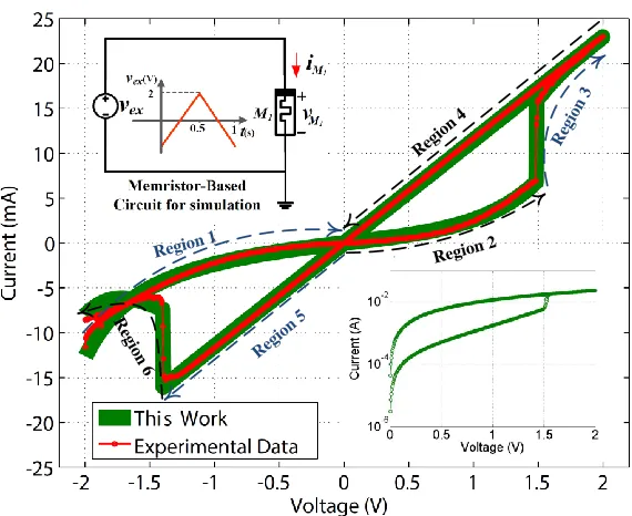
2.4 This plot displays the Ag/TiO2/ITO memristor’s CTM model i-v curve
which has the highest accuracy in comparison with the previous works.
The memristor i-v curve is divided into six regions with different voltage
domains. The CTM model parameters are the same as parameters applied
in Table 2.2. Thisi-v curve is for a±2 V, 1 Hz triangular wave input
volt-age. The bottom right corner inset displayed logarithmic scale i-v curve
2.5 Memristor SPICE model schematic diagram. The memristor SPICE model
has three nodes. Node 1 and 2 represent the positive and negative nodes of
the memristor device, The nodenLis for visualizing the number of oxygen
deficiencies near the Schottky barrier region. . . 48
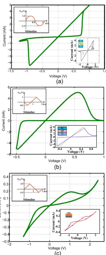
2.6 Proposed CTM model simulations in comparison with fabricated devices
experimental data. In (a) the proposed CTM model fits the experimental
data of the Pt/TiO2/Pt memristor [2] and the model parameters areL= 50
nm, T = 300 K, nth = 0.9, n1 = 0.83,∆Eac = 1.48, Eb = 3.7, E0 =
2×10⁻⁷, E
0M= 0.49, ND = 3.16×10¹⁷, NC = 3.6×10¹⁷, aM = 0.2, ζ =
0.2, bn = 0.17, S = 450. The input voltage applied to the device is
dis-played in the sub-window. In (b) the proposed CTM model fits the
ex-perimental data of the Pt/Hf/Ti memristor [33] and the model parameters
are L = 10 nm, T = 300 K, nth = 0.91, n1 = 0.88,∆Eac = 1.2, Eb =
2.5, E0 = 2×10⁻⁷, E0M = 3.3, ND = 1×10¹⁸, NC = 5 ×10¹⁷, aM =
0.03, ζ = 0.1, bn = 0.6, S = 100. The input voltage applied to the
de-vice is displayed in the sub-window. In (c) the proposed CTM model fits
the experimental data of the SrTiO3 based memristor [34] and the model
parameters are L= 500 nm, T = 300 K,nth = 0.97, n1 = 0.95,∆Eac =
1.15, E0 = 1×10⁻⁶, E0M = 1.2, ND = 7×10¹⁸, NC = 5×10¹⁸, aM =
0.01, ζ = 0.3, bn = 0.06, S = 60. The input voltage applied to the device
2.7 These plots illustrate the fabricated Ag/TiO2/ITO memristor’s accurate
mod-eling and SPICE simulation. The plot in (a) shows that the i-v curve
demonstrates a close match to the experimental data and (b) the
triangu-lar input voltage. The plot in (c) displays the behavior of thenLparameter
versus time and (d) shows the memristor current. The plot (e) shows the
behavior of the nL parameter versus voltage. Lastly (f) plot displays the
Ag/TiO2/ITO memristor model behavior for a±1 V sinusoidal input
volt-age of different frequencies. . . 52
2.8 The Ag/TiO2/ITO memristor’s accurate model is simulated for three input
waveforms. The first row shows subplot for different input voltages and
currents of the memristor. The second and third rows of subplot shows the
number of oxygen deficiencies near the Schottky barrier versus time and
voltage, respectively. The lowest shape illustrates thei−v curve. In (a) a
1 Hz frequency sinusoidal input pulse with 2 V peak to peak amplitude and
0 V DC offset voltage is used, in (b) a±2 V triangular input pulse with a
1 Hz frequency is used, and in (c) a±1.2 V square input pulse with a 1 Hz
frequency is used. . . 55
3.1 Equivalent memristive circuit schematic for Hudgkin Huxley neuron model.
The I-V curves for memristor devices that model sodium and potassium
channels are displayed. . . 66
3.2 (a) Hudgkin Huxley membrane voltage for 15 µA/cm2 stimulus current.
(b) Sodium and potassium channel currents. The parameters were taken
from original paper [9]. (c) Sodium and potassium channel currents versus
membrane voltage. (d) Hudgkin Huxley neuron state variables behavior. . 68
3.3 STDP learning mechanism is illustrated for two coupled neurons with a
memristive synapse in proposed SNN architecture. The memristive
3.4 The membrane voltage of pre and post synaptic Hudgkin Huxley neurons
connected with memristive synapse for 15µA/cm2 stimulus current. . . 71
3.5 2×2 network architecture of the proposed SNN. The input patterns for the
proposed network are defined. . . 73
3.6 The membrane voltage of the pre synaptic (black curve) and post synaptic
(blue curve) neurons for 2×2 network. The proposed network classifies the
patterns successfully. . . 74
3.7 The weight evolution of the memristive synapse for 2×2 network. . . 74
3.8 4×2 network architecture of the proposed SNN. The input patterns for the
proposed network are defined. . . 75
3.9 The membrane voltage of the pre-synaptic Hudgkin Huxley neurons. . . 76
3.10 The membrane voltage of the post-synaptic Hudgkin Huxley neurons. The
weights evolution of the memristive synapses are displayed in bottom graph. 77
4.1 Equivalent circuit schematic for ML neuron model. . . 81
4.2 Equivalent memristive circuit schematic for ML neuron model. . . 83
4.3 Memristive behavior of potassium and calcium channels for ML model is
displayed for2.5V sinusoidal voltage input wave in different frequencies.
(a) Potassium channel memristor i−v for 5 Hz. (b) Potassium channel
memristor i−v for 50 Hz. (c) Potassium channel memristori−v for5
KHz. (d) Calcium channel memristori−vfor100 Hz. (e) Calcium channel
memristori−v for 500 Hz. (f) Calcium channel memristori−v for 50
KHz. . . 85
4.4 The scaled ML neuron bifurcation behavior for different current
stimu-lus. The membrane voltage, calcium channel’s current, potassium
chan-nel’s current and state variables (M, N) are analyzed in each case. (a) The
stimulus current of 60 µA. (b) The stimulus current of 100 µA. (c) The
4.5 STDP learning mechanism is illustrated for two coupled ML neurons with
a memristive synapse. LTD and LTP phenomenons are displayed. . . 89
4.6 2×2 network architecture of the proposed SNN. The input patterns for the
proposed network are defined. . . 91
4.7 The membrane voltage of the pre-synaptic (black curve) and post synaptic
(purple curve) neurons for 2×2 network. The proposed network classifies
the patterns successfully. . . 92
4.8 The weight evolution of the memristive synapse for 2×2 network. . . 93
4.9 The voltage over each memristive synapse that produce LTP or LTD
phe-nomenons for 2×2 network. . . 94
4.10 4×2 network architecture in memristive crossbar array for the proposed
SNN. The input patterns for the proposed network are defined. . . 95
4.11 The membrane voltages of the pre-synaptic neurons for 4×2 network. . . . 96
4.12 The membrane voltage of the post-synaptic neurons for 4×2 network. . . . 96
4.13 The weights evolution of the memristive synapses for 4×2 network. . . 97
5.1 Programming memristor device by applying a0.8 Vsquare pulse with
dif-ferent pulse widths. . . 103
5.2 The schematic of CVNS adder circuit and configuration table for the switches.
(a) Configuration table. (b) MCVNS adder. . . 105
5.3 Different MCVNS adder configurations equivalent circuits. (a) Addition
configuration. (b) Modulo configuration. (c) Modulo circuit for analysis.
(d) Mapping circuit. . . 107
5.4 The voltage over theOUTdevice. (a) The voltage of the output device in
[2RLRS, RHRS] interval for addition configuration. (b) The voltage of the
output device in (RHRS,2RHRS]interval for modulo configuration. Also,
5.5 The simulation results for functionality of MCVNS adder and its relative
error. (a) Two addition operations with the MCVNS adder for radix-10
dig-its. The circuit configured to addition configuration and behavior of state
variable w is depicted for these additions. (b) Addition in modulo mode.
The dotted and solid lines show the cases with programmed resistance with
mapping circuit and theoretically extracted ideal resistance. (c) Relative
error for modulo configuration. . . 110
6.1 (a) Memristor-based crossbar structure. (b) Ideal VCM memristor I-V
curve with different voltages for memristor switching between LRS and
HRS. . . 115
6.2 (a) IMPLY truth table. (b) Schematic of memristor-based IMPLY logic gate. 117
6.3 (a) SET time behavior by sweeping voltage andni. (b) RESET time
behav-ior by sweeping voltage andni. . . 119
6.4 (a) FA design for 4:2 compressor. (b) XOR/MUX design. . . 120
6.5 (a) FA design for 4:2 compressor. (b) XOR/MUX design. . . 123
6.6 (a) FA design for 4:2 compressor. (b) XOR/MUX design. . . 123
7.1 The schematic of logic circuits. (a) NOR gate. (b) NAND gate. . . 131
7.2 The Schematic of the proposed logic gates. (a) OR gate. (b)AND gate. (c)
NOT gate. (d) COPY circuit. . . 134
7.3 The proposed architecture. (a) Block diagram of the proposed architecture.
(b) Mirrored memristive crossbar architecture. . . 136
7.4 The simulation results are for following logic gates: (a) NOR gate. (b) OR
gate. (c) NOT gate. (d) NAND gate. (e) AND gate. (f) COPY circuit. . . . 141
7.5 Multiple fanouts and simulation results for each output. . . 143
7.7 The simulation results for XNOR implementation on two mirrored
2.1 The memristor i-v curve is divided into six regions with different voltage
domains and limited current mechanisms for a±2 V triangular input
volt-age with 1 Hz frequency. . . 47
2.2 Accurate memristor model spice code with charge transport mechanism
analysis. The code is written in HSPICE software. . . 49
2.3 The relative root mean square errors of various memristor models with the
experimental data collected for Ag/TiO2/ITO memristor as±2 V, 1 Hz
tri-angular wave input voltage applied to the device. . . 59
3.1 Scaled Hudgkin Huxley neuron parameters. . . 70
3.2 Memristor device parameters for simulation. . . 70
4.1 Scaled Morris-Lecar neuron parameters. . . 87
4.2 Memristor device parameters for simulation. . . 91
5.1 radix-10CVNS digits of an arbitrary valuex= 73.421. . . 101
5.2 radix-10CVNS digits for addition two arbitrary valuex = 58.34andy =
72.89. . . 102
5.3 Memristor device parameters for simulation. . . 103
5.4 Corresponding memristance for radix-10 CVNS digits withψ = 2resolution.109
6.1 Material implication logic applied voltage sequence for case 1. . . 118
6.2 Material implication logic applied voltage sequence for case 1. . . 119
6.3 Memristor-based MUX computational steps. . . 121
6.4 Memristor logic states for proposed MUX in each step. . . 121
6.5 Computations are shown for each step of memristor-based 4:2 compressor
operation. . . 124
7.1 The operation principles for OR, AND, NOT and COPY circuits for
differ-ent input combinations. . . 137
7.2 Delay and output final state absolute error for each gate. . . 142
7.3 Design constraints forVCOND in proposed logic gates. . . 142
7.4 The 16-bits words for voltage controller select signals in each step for
ANN Artificial Neural Network.
CAD Computer Aided Design.
CBRAM Conductive Bridge Random Access Memory.
CMOS Complementary Metal-Oxide-Semiconductor.
CVNS Continuous Valued Number System.
DRAM Dynamic Random Access Memory.
FA Full Adder.
HH Hudgkin Huxley.
HRS High Resistance State.
IC Integrated Circuit.
IF Integrate and Fire.
IMPLY Material Implication Logic.
LIF Leaky Integrate and Fire.
LTP Long Term Potentiation.
LTD Long Term Depression.
LRS Low Resistance State.
MAGIC Memristor Aided Logic.
MIM Metal Insulator Metal.
ML Morris Lecar.
MSIM Metal Semiconductor Insulator Metal.
MUX Multiplexer.
NMOS n-Channel MOSFET.
PCRAM Phase Change Random Access Memory.
RMS Root Mean Square.
RRAM Resistive Random Access Memory.
SNN Spiking Neural Network.
SRAM Static Random Access Memory.
STDP Spike Timing Dependent Plasticity.
STT-MRAM Spin Transfer Torque Random Access Memory.
TEAM Threshold Adaptive Memristor Model.
TSMC Taiwan Semiconductor Manufacturing Company.
VCM Valence Change Mechanism.
VLSI Very-Large-Scale Integration.
XNOR Exclusive-NOR.
Introduction
M
EMRISTOR (memory-resistor) is a two-terminal device which attracts significant amount of interest by the researchers recently due to its unique characteristics.Its unique i− v curve shows a device with memory and variable resistance that makes
it an interesting element for future computing and memory systems. Its non-volatility,
low power and high switching speed promise an alternative solution for conventional high
speed Static Random Access Memory (SRAM) and Dynamic Random Access Memory
(DRAM). It does not have a leakage power due to its non-volatile behavior, which makes it
a suitable candidate for Flash memories. Also, this device can implement logic in addition
to its memory features and this can provide an architectural solution for future
comput-ing systems. Memristive computcomput-ing systems can provide logic within the memory in the
same platform, which has the potential to change the current Von-Neumann computing
paradigm. In addition to these features, memristor devices are believed to be able to mimic
biological synaptic behavior and reproduce Long Term Potentiation (LTP) and Long Term
Depression (LTD) phenomenon. Utilization of memristive systems have been intensified in
neuro-science research by the experts who are in the quest of building brain-like computers.
Therefore, with these features memristors can be applied for wide ranges of applications.
applications and the thesis outline.
1.1
Definition of Memristor
Until 2008, it was believed that there are only three fundamental passive circuit elements,
capacitor (1745), resistor (1827) and inductor (1831). Although by 1960 Widrow [1]
pro-posed the first concept of memory resistor device which was namedMemistor, the
three-terminal device with the ability to control its memristance by the time integral of current
passes through the device, this device was not considered as fundamental element in circuit
theory. Later in 1971, Leon Chua theorized that the fourth fundamental element named
Memristorshould exist based on the symmetrical relationship between voltage (v), current
(i), charge (q) and flux (Φ) [2]. As it can be seen in Fig. 1.1, this device would complete
the circle where the resistor holds relation between voltage and current (f(v, i) = 0), the
inductor holds relation between current and flux (f(i,Φ) = 0wherev = ddtΦ andΦ = Li),
the capacitor holds relation between voltage and charge (f(v, q) = 0) and the memristor
holds relation between charge and flux (f(q,Φ) = 0). Chua, based on the mathematical
analysis, predicted that a solid-state device (memristor) should exist to make a connection
between charge and flux. Later, he developed the idea of memristor to broader class which
is called memristive devices and systems while a memristor is only a special case in this
family [3]. In 2008, the first physical realization of a memristor device was realized in HP
lab by Dr. Strukov [4]. The device structure was composed of a doped titanium dioxide
(TiO2−x) thin film which was sandwiched by two platinum (Pt) electrodes. The doping is
performed by creating positively charged oxygen vacancies over the length of TiO2film by
removing the negatively charged oxygen atoms from their position in crystallization stage.
By applying an electric field over the device, oxygen vacancies tend to move along the
length of the film and it results the alteration in the conductivity of TiO2 film. Therefore,
Figure 1.1: The fourth missing fundamental circuit elements [4].
Pt Pt
Ti
O
2
Ti
O
2
-x
w L
Oxygen Vacancies
Figure 1.2: The TiO2-based device and its doping profile behavior is displayed.
the device [4]. Also, the oxygen vacancies will remain in their position as the electric field
is removed from the device which shows non-volatility behavior of it. The TiO2-based
device is presented in Fig. 1.2. In 2009, Di Ventra extended the definition of memristor
and memristive systems to capacitor and inductor by defining the terms,meminductorand
memcapacitorwhich are history dependent elements [5]. Memristor device’s i-v curve is
a hysthersis loop which shows variable resistance between High Resistance State (RHRS)
profile is not spread along the film length and the un-doped region covers the whole length
of the device. On the other hand, the high resistance state is when the oxygen vacancies
are migrated through the length of the device and cover the whole length of the film. The
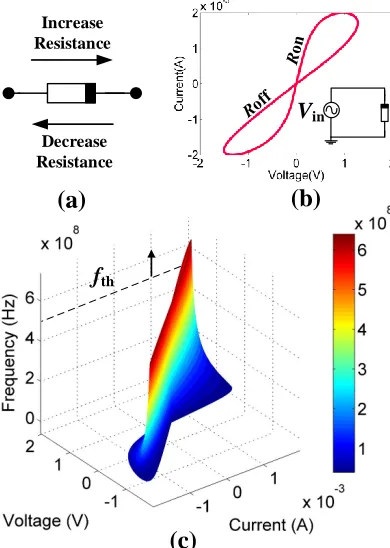
memristor symbol used in this thesis is displayed in Fig. 1.3(a). The polarity of the device
is recognized by a thick black bar. As it can be seen in this figure, the resistance of the
de-vice decreases when the current goes through the bar side and it is increasing when current
enters the device from non-bar side. HP proposed a model [4] for memristor and considers
the variable length of the doped region along the device as the internal state variable (w).
The device is in high resistance state when w = 0 and it is in low resistance state when
w = L(Lis the total length of thin film). Memristor device characteristic can be defined
by the following equations:
i=g(w, v)·v, (1.1)
dw
dt =fv(w, v). (1.2)
These equations refer to the voltage-controlled memristor devices. iandv are the
cur-rent and voltage over the memristor device, respectively. Parameterswis the internal state
variable of the device and based on the HP model, it is in the domain of 0 ≤ w ≤ L.
Also, functiong(·)is the memristor’s conductance which is namedmemductance.
Current-controlled memristor devices characteristics can be defined by,
v =R(w, i)·i, (1.3)
dw
dt =fi(w, i). (1.4)
FunctionR(·)refers to the resistance of the memristor which is namedmemristance.
Mem-ristor is any two terminal black box that follows these equations and have hystheresisi-v
curve which alters in shape by changing the excitation frequency over the device.
fth
Decrease Resistance Increase Resistance
(a) (b)
(c)
Vin
Figure 1.3: (a) The memristor symbol and its behavior toward different current directions enter the
device. (b) Hystheresis loop in low frequencies. (c) The frequency behavior of i-v curve of the
device.
shown that by increasing the excitation frequency the hystheresis loop begins to shrink and
it becomes a single line as the frequency goes beyond specific threshold (fth). Memristor’s
i-v curve behavior by altering frequency is displayed in Fig. 1.3(c). This speed limit
fea-ture can be applied in READ operation of the memristor devices to avoid unwanted state
changes in the device.
1.2
Memristor Modeling
Since 2008 due to exciting discovery of memristor device, significant amount of research
has been devoted in the search for novel materials and structures to manufacture these
the behavior of the device for simulation and development of memristive circuits and
sys-tems. In addition to acceptable accuracy and computational efficiency, the proposed model
should be compatible with commonly accepted design modeling packages like SPICE.
Fol-lowing the recent advancements in the memristor and memristive systems and applications,
several models have been developed for implementation in SPICE-like simulators for
de-signing and simulating the future analog and digital systems based on memristor [14–30].
The very first efforts for modeling memristor [4] presented a linear ion drift model of
mem-ristor which is a physical model derived from mathematical equation of HP 2008 fabricated
memristor. HP memristor was consisted ofTiO2 thin film sandwiched between two
plat-inum electrodes. Deficiency in oxygen atoms in one side ofTiO2 makes a doped region
of the film (TiO2−x). This kind of doping makes two regions with different resistance in
series (doped region: low resistance, undoped region: high resistance). Since the oxygen
vacancies have low mobility by removing the bias over the titanium oxide film they have
the tendency to remain at their current place. Memristors saving information capability by
means of its resistance makes it a non-volatile memory. Effective resistance of the thin
film is related to the boundary position of the regions. The boundary position between the
doped and un-doped regions is proportional to the place of the dopants which is determined
through dopants velocity. Position of the boundary region can be determined through its
velocity (vD).
vD = lim
∆t→0
∆w
∆t =
dw
dt (1.5)
Linear form of the velocity of dopants (vD) equation is the reason for calling this model,
linear boundary drift model. It is determined by,
vD=
ηµDRLRS
L
RLRS RHRS
w
Equivalent Circuit
Figure 1.4: The linear ion drift model equivalent circuit forTiO2-based device.
where L is the length of the film, η shows the memristors polarity and µD indicates the
mobility of dopants and as mentioned before, the memristor is considered as two series
resistors which have high and low resistances. The doped region has low resistance (RLRS)
while the undoped region shows high resistance (RHRS). Boundary region is moved along
theTiO2 film. Therefore, the memristance for aTiO2 memristor with boundary position
ofwless than its films thicknessLcan be determined through:
Rw =RLRS
w
L +RHRS
1−w
L
. (1.7)
Schematic illustration of the linear boundary drift model for Ag/TiO2/ITO memristor is
depicted in Fig. 1.4. Consequently, thei-v relationship is determined by,
i(t) = v(t)
Rinit q
1− 2ηµDRLRS∆Rφ(t)
D2R2
init
. (1.8)
where the parametersRinitand∆Rare given by,
∆R=RHRS−RLRS (1.9)
Rinit =RLRS
w0
L +RHRS
1− w0
L
(a) (b)
f(w) f(w)
w/L w/L
Figure 1.5: The behavior of window function 1 and 2 which are defined in [19] and [18] are
consid-ered for two differentpvalues. (a) Thep= 1is set for the window function 1 and 2. (b) Thep= 7
is set for the window function 1 and 2.
Position of the boundary region varies along the length of TiO2 film. In linear ion drift
model, Eqn. 1.6 shows that the velocity along the whole film thickness has linear behavior,
while the maximum pace of the dopants occurs at the middle point of the film. Due to the
non-linear characteristic of the dopants movement, different window functions (f(·)) were
proposed to insert non-linearity into velocity,
vD=
ηµDRLRS
L · ×f(w)×i(t) (1.11)
For the purpose of decreasing the dopants velocity at the edge of the film and having the
maximum speed at the middle in [19], the non-linear phenomenon takes into account.
fw = 1−
2w
L −1
2p
(1.12)
where, p has a positive value. Power of the above equation adjusts non-linearity in the
velocity of dopants. By increasingp, the linearity rate is soared and this is demonstrated in
model. After setting memristor to its terminal statesRLRSorRHRSwhere window function
1 has zero value [19], changing its state to another value becomes impossible [17]. The
second problem with using this window function is, its weakness for showing the
asym-metric switching behavior. It uses the same behavior pattern for both zero to one and one to
zero transitions ,which may not be the case based on experimental results for ON and OFF
switching [20]. While these mentioned obstacles do not satisfy with window function in
Eqn. 1.12, the following function was proposed which meets the above requirements [18],
fw = 1−
w
L −stp(−i)
2p
(1.13)
In the above equation, i is the memristors current. The maximum value of this window
function is limited to one and cannot be adjusted to the values less or more than one.
Therefore, in this window function the scale factor has been added for the purpose of having
adjustable maximum value for the state variable [23],
fw =j
1−
w
L −1
2
−0.75
p
(1.14)
where j is scale factor. It controls the maximum value of the window function. This
window function [23] as is depicted in Fig. 1.6, has different maximums which are lower
or upper than one. In addition, the hyperbolic sine behavior has been noticed between
the changing rate of the differential conductance and the applied voltage at low electric
field relative to the tunneling barrier width [31]. While those window functions satisfy
the boundary problems the linear ion drift model cannot fully reproduce the non-linear
behavior of the device. Additionally, the common problem in former models is that there
(a) (b)
f(w)
w/L w/L
f(w)
Figure 1.6: The window function 3 [23] can adjust its amplitude through the scale factor j. (a)
Three figures of window function 3 [23] with the samep= 1, and three different scale factor values
(j = 0.75, j = 1, j = 1.5). (b) Three figures of window function 3 with the samep= 7, and three
different scale factor values (j= 0.75, j = 1, j = 1.5).
presented,
dw
dt =a×f(w)×g(v) (1.15)
i(t) = w(t)nβsinh(αv(t)) +χ(exp(γv(t))−1). (1.16)
whereg(v) = v(t)mandmis an odd integer. Also,ais a constant parameter. The velocity
equation shows nonlinear relation to voltage. The differential parameters areα, β, γ and
χ which can be determined through experimental data. In the above equation, n is a
pa-rameter which demonstrates the impact of the state variable over the memristor’s current.
wparameter is the normalized state variable which has a value between 0 and 1. This state
variable is approximately equal to one in ON state. When the memristor has the lowest
memristance the second expression,χ(exp(γv(t))−1), has a negligible value in
compar-ison with the first part,βsinh(αv(t)), which defines the tunneling phenomenon. When the
(a) (b)
Figure 1.7: (a) It depicts Ag/TiO2/ITO memristors linear ion drift model hysteresis plot with an
input voltage source by 2 V triangular wave with 1 Hz frequency in comparison with the memristors
measured experimental data [20].(b) This shows linear ion drift model of Ag/TiO2/ITO memristor
by proposing window function 3.
ideal diode. Another model can be defined by [32],
Asign(v(m)exp(|vM|
v0 −exp(
vT H
v0
|vM|> vT H
0 otherwise
(1.17)
where vTH and vM are the threshold and the applied voltage, respectively. This equation
consists of signum function, and v0 may depend on the velocity of dopant or be
inde-pendent. In the high resistance state of memristor the velocity of the dopants is assumed
0 which is an ideal value as the applied voltage is less than the threshold voltage. The
Ag/TiO2/ITO memristors nonlinear model is shown in Fig. 1.8 in comparison with the real
measured data in laboratory. In the non-linear ion drift modeling of memristor like the
lin-ear ion drift modeling, the memristor doped and undoped region considered as two series
resistor. In [14], a new assumption of memristor for modeling is presented. In this model,
memristor is considered as a resistor in series with an electron tunnel barrier. As it is shown
−2 −1.5 −1 −0.5 0 0.5 1 1.5 2 −0.02 −0.015 −0.01 −0.005 0 0.005 0.01 0.015 0.02 0.025 Voltage(V) Current(amp)
Non Linear Model (Window Function 3) Experimental Data
Non Linear Model (Window Function 1)
Figure 1.8: This shows nonlinear ion drift model of Ag/TiO2/ITO memristor by proposing window function 1 and 3.
velocity can be determined by [14],
dx dt =
cof fsinh(iof fi exp
−exp
x−a
of f
wc −
|i|
b
− x
wc
i >0
consinh(ioni exp
−exp
x−aon
wc −
|i|
b
− x
wc
i <0
(1.18)
Fitting parameters arecof f,con,aof f,aon,iof f,ion,wcandb. cof f,conadjust the magnitude
ofxderivative change whileconis larger about an order of magnitude thancof f. Since this
model provides a programming threshold, iof f and ion are the quantities for limiting the
threshold current. Changing in state variable derivative is desired for higher current than
the threshold current. Theaof f andaondefines the upper and lower bound interval for state
variablex. Therefore, thex−aof fand(x−aon)are negative quantities. Subsequently, since
the exponential function is used in this equation and the negative value of its variable, a
the different ON and OFF switching pace which fits the experimental results as well. The
current voltage relationship in this model defined as follow [14],
vg =v−i(t)Rs, (1.19)
where vg is the voltage of un-doped region and v is the internal voltage on the
memris-tor which is differed from the applied voltage on memrismemris-tor. A SPICE model of simmons
tunneling barrier model is proposed in [15]. Although it has complexity and high
computa-tional time, it brings the highest accuracy in comparison with the other models. This model
is shown in Fig. 1.9, for Ag/TiO2/ITO memristor in comparison with the experimental
data. The other good model is [33] which is based on a piece wise modeling approach
which is the subtle function of the rate of change in memristance. In [33], the window
function is eliminated whereas theg(.)function is imposed the tunneling phenomenon and
asymmetric switching behavior to the model,
dx
dt =vx.g(v, ρ(w), φ0), (1.20)
wherevx is a constant which is determined switching pace in xnormalized distance (0,1)
based on experimental data andφ0 is the equilibrium barrier height. ρwis the shape factor
parameter which has a linear dependent to the tunneling junction width. This makes a
high non-linearity in one boundary of memristor and low non-linearity at opposite side
which results dinormalization of the function. The voltage current relationship which is the
modification of thei−vrelation [33],
i(t) =wnsinh(vMϑ) +χ(exp(γvM)−1), (1.21)
wherewandϑ are fitting parameters for defining ON state of the device. χandγ are the
through the first term of this equation. Parameter n is defined the rate of non-linearity
between the drift velocity of dopants and the ON switching current. The higher value
parametern has the non-linearity rate is increased. Like the model in [15], this model is
showed acceptable accuracy and a good adaptation with tunneling phenomena. A more
simplified model [21] with acceptable accuracy in comparison with its former peers was
presented later. In addition of its generality in comparison with Simmons tunneling barrier
model, it uses simpler mathematical functions to achieve the same physical memristive
behavior. Since this model is using polynomial dependence rather than exponential one
which was used in Simmons tunneling barrier model, the TEAM model is becoming more
computationally efficient. The TEAM models derivative state variable is,
dx
dt =
kof f
i(t)
iof f −1
αof f
·fof f(x) 0< iof f < i
0 ion < i < iof f
kon
i(t)
ion −1
αon
·fon(x) i < ion <0
(1.22)
Theionandiof f are the current thresholds andkof f, kon,αof f andαon are constants. The
effective electric tunnel width which is considered as an internal state variable is
repre-sented byx. The window functions arefonandfof f which limit the internal state variable
to [xon , xof f] interval. Like Simmons tunnel barrier asymmetric behavior, fon and fof f
may have different values. This model shows an acceptable accuracy but lower than
Sim-mons tunneling barrier model. In Fig. 1.9, the Ag/TiO2/ITO memristors experimental data
has compared with the TEAM models simulation data. Later on, a voltage-based model is
also presented with the same method [27]. Beside the mentioned predictive models in the
literature, model in [26] was proposed based on fitting to an experimentally measuredi−v
curve from a fabricated memristive device. The compact model [26] based on experimental
observations were developed to account for irregulari−v characteristics. In this work, a
(a) (b)
Figure 1.9: (a) It depicts Ag/TiO2/ITO memristors simmons tunnel barrier model which has the
highest accuracy in comparison with the other predictive models. (b) It depicts Ag/TiO2/ITO
mem-ristors TEAM barrier model.
is presented. Although this model has demonstrated better accuracy in comparison with
the predictive models, it does not present a comprehensive template for modeling various
memristive devices and it also needs mathematical computations to find the model
param-eters for every memristive device. One of the other model is presented in [24], is known
as generalized memristive device model. In this work, by utilizing several mathematical
functions, behaviors of the memristor devices are simulated based on their physical
prop-erties. Although the model in [24] is a general model which is simple and it can be used in
large-scale computations, it cannot reproduce the non-linear device behavior in high
resis-tance state. Also, this model in not fully established based on the physical charge transport
mechanism of the memristor devices. The simulation of generalized model is displayed in
Fig. 1.10
1.3
Memristor Crossbar
One of the most promising structure developed by memristor devices is crossbar
−2 −1.5 −1 −0.5 0 0.5 1 1.5 2 −25
−20 −15 −10 −5 0 5 10 15 20 25
Voltage (V)
Current (mA)
Generalized Model Experimental Data
Figure 1.10: This plot displays how the generalized memristor model [24] is able to match the
Ag/TiO2/ITO-based memristor data.
systems. As it can be seen in Fig. 1.11, a memristor crossbar is a connected structure that
comprises of a matrix of memristors connected with metal wires. Each device is connected
to a top horizontal metal wire and a vertical bottom wire. The crossbar structure provides
the highest possible integration density of memristor devices within a single layer, in which
each memristor uses4F2 circuit area whereF is the minimum feature size.
One of the most important issue in memristor crossbar array is the problem of sneak
path currents [36]. This can affect the functionality and performance of the system. As
an example in READ operation, due to several alternate current paths in a regular crossbar
array an exact value of stored value in cell cannot be READ properly. To avoid these
issues, several approaches were proposed by the researchers [37, 38]. These solutions are
in device and architectural level. In the device level, a complementary resistive switch
(CRS) was proposed with specifici−v characteristic [37]. This device comprised of two
m
iji-th
j-th
y
x
Figure 1.11: READ operation in memristor crossbar architecture.
high resistance state which considerably reduces the alternate current paths in crossbar.
Beside the device level solution, modification in the architecture of the memristive
crossbar systems can provide lower sneak path effect. In [39], an access transistor was
added over each memristor device which isolates other unwanted devices and mitigate
al-ternate current paths. This crossbar architecture is called 1T1R architecture and its main
drawback is its low density due to the large area needed for access devices. The other
archi-tecture is 1TNR [40] archiarchi-tecture which is utilized only one access transistor for all devices
in each row. This architecture has higher density in comparison with 1T1R and provides
acceptable sneak path current mitigation rate.
The READ operation in crossbar for each device can be done individually. For example,
when reading the resistance of memristor mij connecting to i-th top metal wire and j-th
bottom metal wire, a sensing voltagev will be applied oni-th top wire and all of the other
wires are grounded. The currentcj can be sensed from j-th metal wire and resistance of
GND GND
GND GND
VW/2 -VW/2 VW/2 -VW/2 VW/2 -VW/2 VW/2 -VW/2
-VW/2
VW/2
(a)
(b)
Figure 1.12: WRITE operation in memristor crossbar (a) Write 1. (b) Write 0.
1.12. This method is a two step process. It writes desired values on entire row of selected
crossbar array. In the first step for writing logic 1 (RLRS) on target devices, a voltage of
VW/2and GND (0 V) are applied to a selected row and all unwanted rows, respectively.
The voltage VW is greater than threshold of the device (> VTH). Also, the columns on
which logic 1 should be connected to−VW/2and a voltage VW/2is applied to the other
columns. The logic 1 will be written over the target devices in this step. In the second step,
the selected row is connected to−VW/2and the voltage of GND is applied to all unwanted
rows. Furthermore, a voltage ofVW/2and−VW/2are applied to the columns which logic
0 should be written on and other columns, respectively. This step will write logic 0 on all
target devices in the selected row.
1.4
Applications of Memristor
Due to the unique features of nanoscale memristor devices, these devices attract researchers
attention to be applied in wide ranges of applications. Memristor can be utilized in several
applications like memory, logic, analog circuits, cryptography, neuromorphic, filter design,
logic and neuromorphic applications to get a better insight about the following chapters of
the thesis.
1.4.1
Memory
One of the important application of memristor device is memory [41]. The non-volatility,
low power, scalability and CMOS compatibility features of memristor device makes it a
promising alternative for conventional SRAM and DRAM memories. Several types of
memories are fabricated based on the memristive behavior. Spintronic memristor
(STT-MRAM) is one of the most promising candidate for future ultra high density and high speed
memories [42]. Spintronic memristor alters its resistance by changing the direction of the
spin of the electrons. Due to the low memristance ratio (RHRS/RLRS) of these devices, an
access transistor should be utilized in crossbar array for each individual memristors. This
limits the maximum size of array’s areal density by the size of access transistor devices.
Phase Change Random Access Memory (PCRAM) is another promising memory
tech-nology. In comparison with STT-MRAM and Resistive Random Access Memory (RRAM)
it has a longer switching time (50 to 100 ns) and it has the lowest endurance in terms
of switching cycles before failure [43]. Therefore, these devices are not considered for
SRAM because of their low switching speed and they can be considered as a replacement
for DRAM cells. The unipolar switching characteristic [44] in PCRAM makes these
de-vices a good candidate for high density design which limiting the sneak path currents can
be provided by using a diode. RRAM [45] is one of the important memory technologies
and its functionality is based on the resistive switching. Unlike PCRAM devices which
uses heat to change resistance state, the resistance of the RRAM device is changed by
ap-plying a voltage across the device. These devices provides high density, low manufacturing
costs, high switching speed and relatively acceptable endurance. Conductive Bridge
Ran-dom Access Memory (CBRAM) [46] is another memory with low current, high resistance
Figure 1.13: Spintronic memristor device schematic. [47].
1.4.2
Logic
Memristor is not only a memory but it has the capability to implement logic which makes
it a unique device for use in future memory and computing systems [48]. These devices
can implement logic within the memory which can be applied for in-memory computing
scheme. Unlike Von-Neumann architecture where the memory and processing units are
separate and there is a constant need for huge amount of interconnections between these
units for constant communication, in-memory computing systems not only requires only
one platform to implement logic and memory but also it does not need the interconnections.
Thus, logic implementation with memristor has been intensified in research and there are
several logic methods [48–50, 50–55] have been designed recently.
Memristor logic implementation methods can be divided based on the digital and analog
property of the device. Memristor can be used as analog memory [53, 55] since it can be
programmed to different memristance values. This opens a new path to explore analog
arithmetic circuits by using the analog memory property of the memristor. Also, logic
implementation of memristor can be applied in digital domain and there are several logic
methods proposed [48–52]. Digital logic implementation with memristor devices can be
categorized into the resistance-based and voltage-based logic methods. In resistance-based
voltage-based logic method the logical state is determined by the voltage level. Therefore,
the resistance-based logic can be applied for in-memory computing scheme while there is
no memory feature in voltage-based logic [51, 52]. In the resistance-based logic the logic
0 corresponds to high resistance state and the logic 1 corresponds to low resistance state.
There are several resistance-based logic method proposed by memristor devices.
IMPLY logic is one of the famous logic implementation method with memristor [48].
This logic is based on IMPLY function which comprises of two input memristor devices and
one resistor. The inputs should be programmed by memristance over the input devices. This
logic is a sequential logic and it requires some steps to finish its computation procedure.
Two voltage levels are required for this logic (VCOND and VSET). IMPLY logic is a pure
memristive logic and it can be implemented on memristor crossbar. The main drawback for
this logic is, its sequential nature which requires several computational steps to implement
large-scale computations. Also, the output is written over one of the input devices and this
results in loosing one of the inputs. Another resistance-based logic is MAGIC [51] and this
logic is a pure memristive logic. Only one voltage level is required to be applied in this
logic. The inputs are the memristance of the input devices. The input and output devices
in this technique are separate. In this method, for some input combinations, input devices’
states are changed during the logic operation and this results in missing the input for next
operation.
Hybrid CMOS/Memristor-based method is another technique to implement logic. MRL
[49] is one of hybrid CMOS/memristor approach which is a voltage-based logic. This
logic suffers from a signal degradation and therefore CMOS buffer is needed to amplify
the output signal level. Also, for creating some logic gates like AND and OR, a CMOS
inverter should be added to the output of NAND and NOR MRL gates. In this logic method,
memristors are worked only as computational element and do not store any value. In this
logic, the inputs are applied as voltage levels to the circuit and the initial memristance of the
step to perform the logic operation.
1.4.3
Neuromorphic
Neuromorphic engineering is a field for designing neural architectures and circuits based
on biological nervous system. Over the past few years, interest in neuromorphic computing
has been increasing significantly [31]. There is a growing need for efficient smaller
hard-ware with powerful data processing capability to implement large scale neural network for
recognition, mining, and synthesis applications. The memristor is attracted significant
at-tention as a potential element for building the neural systems. As it can be seen in Fig.
1.14, it has a similar behavior to a real synaptic connections in brain [56]. Since like brain
synapses which need only electrochemical pulses to alter their weights, memristors require
a voltage pulse for changing its conductivity. Memristor device can mimic a real
biolog-ical synapse behaviors and can reproduce Spike Time Dependent Plasticity Mechanism
(STDP) [57]. STDP consists of two main phenomenon Long Term Potentiation (LTP) and
Long Term Depression (LTD) which generate based on timing difference of the pre- and
post-synaptic spikes.
1.5
Outline of Thesis
This thesis encompasses two main partsPart IandPart II.Part Iis related to the
mem-ristor device modeling andPart II is focusing on memristive computing circuits and
ap-plications. Part IIis divided into different computing schemes (neuromorphic, analog and
digital). This part contains five independent chapters. A background about memristor
def-inition, its applications and a brief review of the selected previous models are presented
in Chapter 1 (introduction). The modeling and its analysis is presented in Chapter 2. The
neuromorphic computing task with memristor is studied in Chapter 3 and 4. Also, an
Figure 1.14: Memristor versus biological synapse [58].
existing memristive digital logic (IMPLY logic). In Chapter 7, a novel memristive logic
is presented along with its novel architecture, summary, conclusion and future works are
presented in Chapter 8.
• Introduction, in Chapter 1, the background information and memristor definition
and its functionality is presented. Also, the memristor crossbar architecture is
ex-plained along with READ and WRITE operation methods within the crossbar on
each device. In the next section, some relevant previous models, window functions
and the modeling evolution are discussed. Then, the significant potential applications
of memristor are explained (memory, logic and neuromorphic).
• Part I- Modeling,in Chapter 2, an accurate model for nanoionic memristive device
is presented. The proposed model is based on the charge transport mechanisms in
structures are discussed. A physic-based model is presented based on charge
trans-port mechanisms existed in schottky barrier region. Also, a SPICE code is developed
for the proposed model and it is tested for various devices to ensure its functionality.
• Part II- Memristive Computing,This part is comprised of 5 chapters. In Chapter 3
and 4, pattern classification tasks are performed by a memristive bio-inspired Spiking
Neural Network (SNN). In Chapter 5, an analog memristive adder is presented with
a Continuous Value Number System (CVNS). This adder is designed based on the
analog property of memristor devices. In Chapter 6, a 4:2 compressor circuit is
designed with IMPLY logic and this implementation is completely optimized. In
Chapter 7, a novel memristive logic paradigm is presented and a mirrored crossbar
architecture has been developed to implement this novel logic. Different logic gates
are also designed and tested with the proposed logic scheme. Also, the mirrored
architecture has been tested by Cadence simulation for a larger combinational logic
function.
1.6
Summary of Contributions
This thesis consists of several contributions which are defined briefly in this section.
Memristor modeling is an important topic in memristive systems research due to the
growing need of circuit designers for an accurate and reliable model which is capable of
reproducing the behavior of a real device. For this purpose a review of the memristor
models is presented in Chapter 1and different models were analyzed. In Chapter 2, a
physic-based accurate model is presented based on the charge transport mechanisms in
schottky barrier region of the memristor devices. This is one of the novel contributions
in this thesis. The proposed model was tested in Matlab to prove its functionality and
it showed an acceptable error in comparison with experimental data extracted from a real


![Figure 1.10: This plot displays how the generalized memristor model [24] is able to match theAg/TiO2/ITO-based memristor data.](https://thumb-us.123doks.com/thumbv2/123dok_us/1367434.1169497/44.612.141.497.104.361/figure-displays-generalized-memristor-model-match-theag-memristor.webp)
![Figure 1.14: Memristor versus biological synapse [58].](https://thumb-us.123doks.com/thumbv2/123dok_us/1367434.1169497/51.612.151.498.110.371/figure-memristor-versus-biological-synapse.webp)
![Figure 2.1: (a) A cross-sectional view of the Ag/TiO2characteristic of the physical Ag/TiO4200-SCS semiconductor parameter analyzer [4]](https://thumb-us.123doks.com/thumbv2/123dok_us/1367434.1169497/63.612.200.447.93.387/figure-cross-sectional-characteristic-physical-semiconductor-parameter-analyzer.webp)