Review on Gate Bias Control Method for RF
Power Amplifiers Using ARM Processor
Iram Nausheen
1, Shireen T. Sheikh
2, Mohsina Anjum
3Assistant Professor, Dept. of ETC, Anjuman College of Engineering and Technology, Nagpur, Maharashtra, India
ABSTRACT: The present paper is a review of the past work done in the field of analysis on various control techniques used in wireless communication to control power amplifier’s important parameters. In wireless applications, the power amplifier (PA) dominates signal-chain performance in terms of power dissipation, linearity, efficiency and cost. Hence on the basis of performance concern of a base station’s power amplifier makes it possible to maximize the output power while achieving optimum linearity and efficiency. This paper discusses the elements of a monitoring-and-controlling solution for the Power amplifiers and for various systems. Failures were observed with the traditional ways of gate voltage control techniques and the failures are because of changes of load with respect to current and temperature being taken in to account and the voltage surges at the load line. With traditional gate control method power dissipation is high. The effects of temperature making the trade-offs between the above mentioned Power amplifier parameters which determine the optimum bias condition for the Power amplifier transistor. The drain current should be maintained at an optimum value over temperature and time that can significantly improve the overall performance of the PA gate bias control system. The use of ARM microcontroller makes the system more efficient, cost effective way and a more efficient control system with the use of real time operations using real time operating system uC/OSII.
KEYWORDS: PA power amplifier, gate voltage, ARM 7, uC/OS-II.
I.INTRODUCTION
In wireless systems, the power amplifiers (PA) are the important elements which are responsible for more than half of their total power consumption. Hence to lower the power consumption and dissipation a control system need to be designed so as to compensate for the losses and for maintaining the device as well. To improve efficiency Power amplifier’s monitoring and controlling in necessary and the system operating cost is reduced and can increase output power and reaches to the highest possible linearity to obtain less distortion and allow the operator to discover and solve problems, thus helps in improving operating reliability and life of power amplifier.[1]
For this the performance parameters of RF PA need to be studied. In order to ensure the performance of RF power amplifier it is important to maintain a constant static operating point to keep its work status stable. A base station’s power efficiency is a key environmental consideration for base stations and its optimization dependency. Necessary efforts are being made to improve the overall energy consumption of base stations to reduce their effect on the environment. Operating system costs in a PA is responsible for more than half of the power dissipation. Thus, PA’s power efficiency can improve the operational performance, and provide environmental and financial benefits.In this paper, a new reference design with respect to changes of temperature and drain current through the real time operating system uC/OS-II system to the main-controller ARM7 to real-time compensate for the differences of the linear MOS Power amplifier at different points of temperature
.
II.LITERATURE SURVEY RF POWERAMPLIFIERSFACTORS
Intercept Point), efficiency and other parameters of power amplifier. In order to ensure the performance of RF power amplifier it is important to maintain a constant static operating point to keep its work status stable. The effect of the temperature on the different DC parameters, gm, Idss, rds(on) and capacitances, and the correlation with the figures of merit of a PA (power capability, efficiency and linearity).[2]
RF power amplifiers (PAs) require more powerful Transistors. Therefore, thermal management then becomes a real challenge. Here are the following characteristics for RF MOS PA which are taken into considerations while changing of parameters.
Fig. 1 Ids versus Vgs for different die temperature
Characteristics curve shows the effects of temperature on the gate voltage.
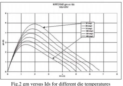
Fig.2 gm versus Ids for different die temperatures
The above characteristics shows the temperature variations and its effects on transconductance.
measurement are used in Cadence RF simulations to examine class-AB PA performances such as output
power Pout, power-added efficiency ηadd, third-order intercept point (IP3), and adjacent channel power ratio
(ACPR) after electrical and temperature stresses.[3] And there are various technologies used for the power control
which can b obtained by various diffusions materials to be used for the construction which ultimately leads to the changes in the composition and the various effects like improvement in transconductance, the break down voltage, reduction in on-resistance and in switching delays as well.[4] The effect of the temperature on the different DC parameters, gm, Idss, rds(on) and capacitances, and the correlation with the figures of merit of a PA (power capability, efficiency and linearity).The drain-to-source current of the LDMOS transistor, IDS, is a function of the gate-to-source
voltage, Vgs, has two temperature-dependent terms:
The effective electron mobility, μ.
The threshold voltage, Vth.
Drain to source current is by the expression:[5]
IDS= 2 ... 1
Vth and μ decrease with increasing temperature. Hence due to the changes in these terms will cause variations in output power. The main factors impacting the drain current bias point are due to variations of the high-voltage supply line and the die temperature. [6]
A better approach is dynamic control of the PA gate voltage which makes use of a control algorithm to be applicable digitally tin order to measure the drain current then digitizing it with an analog to digital convertor, and setting the required bias via a high-resolution digital to analog convertor or a lower-resolution digital pot. Here the system allows the PA to maintain the required bias condition for optimized performance set by a user-programmable set point despite of the changes in parameters.
III.TRADITIONALGATEVOLTAGECONTROLTECHNIQUES
In practical applications, LDMOS power amplifiers operate in Class A or AB, with the positive temperature characteristics near quiescent point. This bias scheme creates a linearization due to the cancellation of Intermodular distortion generated by the carrier and peaking amplifiers.[7] That is, under a certain gate voltage, when working temperature rises, the static current Idq increases, when work temperature decreases, Idq reduces. This determines the need for automatic control of gate voltage for LDMOS amplifier to ensure high efficiency and linear work of RF power amplifier. Earlier at the biasing terminal the load pull transistors were also used which acquires the large space as well as the large power dissipation and the maintainability required for the individual transistors, external transformer for the supply also increases its cost and power consumption is more.[8]
There are traditionally two kinds of gate voltage control technology in practical applications:
The first one is to use temperature compensated components, such as diodes, transistors, voltage regulator ICs, thermistors in the bias circuit, to achieve the gate voltage compensation based on the temperature properties.
IV.EMBEDDEDGATEBIASCONTROLSYSTEM DESIGN
ARM7 (Advanced RISC Machines ) processor is a kind of 32 bit microprocessor having small volume, light weight, low cost and high speed and dependability are its merits compared with industrial control computer and higher speed, multi-functions, low power consumption and well extensibility are its strengths compared with 16 bit single chip. The ARM 7 based CPU LPC2119 was used in the power system, which supports the real-time simulation and embedded-track, and includes many periphery components, such as zero waited 256K in-chip Flash ,16K SRAM(no need extensible memory), UART, hardware I2C,SPI bus, PWM, timer, ADC, CAN field bus controller, all which make it powerful.[9]
There can be three options for implementing a PA control:
A discrete solution
An integrated solution.
Integrated solution based on ARM7 microcontroller
The discrete implementation requires many parts such as a complicated PCB layout and a more circuit design area, all of which lead to higher cost. The integrated solution design has a higher level of compactness, lower cost, and higher reliability, but it needs another device outside the integrated chip a microcontroller (MCU) to control the functions.
Fig3. Shows a complete structure with the help of discrete components can be mounted on a single chip. But here again an external controlling unit is needed. And with the use of these discrete components the task becomes more tedious, since the interfacing and matching should be among each and every device shown in the connection properly and hence the reliability cannot be maintained and if one of the component is damaged the whole system would come to an adverse effect of shutdown. Hence a system should be made with the ARM processor which has inbuilt ADCs and DACs in chip and flash memory also for the storage of tables and it shares many of the benefits of integrated design, but it includes the MCU.
Fig.3 Simplified control system
The temperature and high-voltage supply affects the drain current and this high supply voltage also matters the drain voltage. The RF MOS drain current can be measured with a high voltage current amplifier. If the current at the gate terminal is monitored in a continuous fashion, an operator can make adjustments in voltage at the gate point when a voltage surge occurs on the high-voltage supply to keep the RF MOS working at the best operating point.
performance which can be set by user though the changes in voltage, temperature, and other environmental parameters.[10]
The control and management of the Vgs based on ARM7 is designed by the support of uC/OS-II having better quality of high real-time and adopts real-time multitask kernel which is based on fixed-priority scheduling mode, it could be easily solidified and clipped, getting the high stability and reliability. In addition, the source code of uC/OSII could be shared to make it convenient to transplant and maintain. A lot of system services such as real time tasks are performed as, queues, semaphores, fixed-sized memory partitions, time related functions and etc are offered.[11]
V.CONCLUSION
In this paper different ways of gate voltage control system design and various affecting measures such as temperature and current are found to be the sensitive parameters which are responsible for the hampering effect for an RF PA so among the available method the LUT design using flash memory in ARM processor a feasible one. Still there is an essential need for an efficient monitor and a control system which can be useful for wide range of RF amplification in terms of power , current and with due effects of temperature on this technique with other multiuser software so that accuracy of result could be maintained for better performances. In order to accurately analyse and optimize the, control system there is a need to experiment with temperature and current factors responsible for efficient performance and the maintainability of the device and controlling this with the ARM7 . Hence, from a variety of aspects, such as references, features, hardware and software designs and technologies is being discussed a new reference design can be made using an ARM processor which can be operated at real time measurement using uC/OSII real time operating system and correction of the parameters responsible for affecting the gate bias automatically.
VI.FUTUREWORK
This review suggests that in forthcoming efforts, analysis of different techniques by utilizing the circuit components with temperature compensation, to achieve the gate voltage compensation, but the gate voltage may not be independently regulated through this method. The other one is the using of SCM (single chip microcomputer) and memory storage of tables. In future we explore the failure analysis of discrete components and integrated ones which tends to fail, causes major power losses for base stations. Our future work is to propose a better control technique using controlling algorithms for various readings for concluding the automatic control of gate voltage for RF PA amplifier to ensure high efficiency and linear work and to save energy as well.
REFERENCES
[1] Liang Li, Taijun Liu, Yan Ye,Ying Zhang, Jun Li.,”Embedded ARM-Based Automatic Gate Bias Control System for LDMOS RF Power Amplifiers”, IEEE 2011.
[2] Olivier Lembeye and Jean-Christophe Nanan.”The Effects of Temperature on High-Power RF LDMOS Transistor”. Motorola SPS. Technical feature ,August 2002 .
[3] Chuanzhao Yu, J. S. Yuan,”Electrical and temperature stress effects of Class-AB Power Amplifier Performances”, IEEE transactions on electron devices, vol. 54, no. 6, June 2007
[4] Radhakrishnan Sithanandam et.al.” A new HSG SOI LDMOS for RF power Amplifier applications”.VLSI design conference.2010 [5] WANG et al. IEEE journal of solid-state circuits, vol. 29, July1994.”MOSFET thermal noise modeling for analog integrated circuits” [6] Liam Riordan,” Analogue dialogue.2008.Discrete- and Integrated Control of Power Amplifiers”, April 2008
[7] Jeonghyeon Cha et.alBias,” Controlled Power Amplifier with a Load-Modulated Scheme for High Efficiency and Linearity”, IEEE. 2003 [8] Cheng-Yung Chiang and Huey-Ru Chuang,” Effective Load-Pull System for transistor Large-Signal Measurements for wireless systems”
,IEEE transactions on instrumentation and measurement, vol 46,October 1997.
[9] Hao Jianmin, Guo Kai, Cheng Hong, Ren Na. 2007,” Design of Microoxidation power control system based on LPC2119”, Conference Electronic Measurement and Instruments, 2007
[10] Daogang Peng, Hao Zhang, et.al.” Research and Development of the Remote I/O Data Acquisition System Based on Embedded ARM Platform”, 2009.