Design & Analysis of 8GHz X-Band
Micro strip Patch Antenna
Tanwy Barua1, M. Tanseer Ali2
MEEE, American International University-Bangladesh, Bangladesh1
Assistant Professor, Dept. of EEE, American International University-Bangladesh, Bangladesh2
ABSTRACT: The study of micro strip patch antennas has made great progress in recent years. Compared with conventional antennas, micro strip patch antennas have more advantages and better prospects. They are lighter in weight, low volume, low cost, low profile, smaller in dimension and ease of fabrication and conformity. Moreover, the micro strip patch antennas can provide dual and circular polarizations, dual-frequency operation, frequency agility, broad band-width, feed line flexibility, and beam scanning omnidirectional patterning. In this paper we discuss the micro strip antenna, types of microstrip antenna, feeding techniques and application of micro strip patch antenna with their advantage and disadvantages over conventional microwave antennas. We simulated for radiation pattern up to 1.8. Our antenna height 2.88 mm after simulation we got frequency 2GHz. From simulation patch antenna resonating at 1.8 having a return loss of -12.5dB and those -3dB and -10dB bandwidths are 0.74GHz and 0.25GHz, due to the reason that the radio amplifier reduces the output power, can be more worse and can become unstable if the VSWR is large.
KEYWORDS:Duroid, FR4, H-plane, E-plane, CST Studio, ABS Box.
I.INTRODUCTION
Recently, various machining techniques, including multilayer printed circuit board (MPCB), complementary metal oxide semiconductor (CMOS), low-temperature coffered ceramics (LTCC), and micro-electromechanical systems (MEMS), are highly developed, opening opportunities for innovative antennas, such as active antennas, reconfigurable antennas, met material-based antennas, THz antennas, and so forth [1]. With the availability of precision and high-speed advanced machining techniques, Micro-strip antennas are growing towards highly integration of antenna/array and feed network and operating at relatively high frequencies [1]. Since they are all based on the advanced machining techniques, we suggest that a third research area of Micro-strip antennas is constantly introducing novel advanced machining techniques. In the following, two examples will be presented to show how important the advanced machining technique is to fabricate Micro-strip antennas [2]. One is the highly integrate broad-bandMicro-strip antenna array fabricated using MPCB technology. Another is THz wave planar integrated active Micro-strip antenna using MEMS technology. Recently, with the development of the multilayer printed circuit board (MPCB) technology, the Micro-strip antennas can be designed and fabricated from one-dimensional (1D) to 2D and even 3D structures. Antenna consists of a parasitic patch, a driven patch, a strip line feeding network, a broad-band coaxial line to strip line transition, some buried screw holes, and some via holes. The feeding network is integrated in the bottom of the substrate of the antenna. As all of the structures fabricated at once, the accuracy and the uniformity can be assured. Two antennas of this type are measured.
II. DESIGN METHODOLOGY
into space is accomplished with the aid of specially designed structures called antennas. If the time varying current density established on an antenna structure is unknown, the radiated fields can be calculated without great difficulty. A more difficult problem is determination of current density J on an antenna such that the resultant field will satisfy the required boundary conditions on the antenna surface. In many practical antenna structures it is often possible to estimate the current distribution with sufficient accuracy to obtain good approximation of radiated fields. However, in order to calculate the impedance properties of an antenna, the current distribution is required to be known with higher accuracy. As we have mentioned that if the time varying current density J on the antenna is known, the radiated E and
H fields can be determined. Necessary equations:
Fr=
( ∆ )√
___________________________(1)
ɛr=
ɛ+
ɛ(1 +
)
/____________________________(2)
∆
Wy= 0.412
(ɛ . )(
. )
(ɛ . )( . )
_______________________ (3)
Where, C= 3×10 m
Fr= Resonant Frequency
ɛr= Effective dielectric constant
∆Wy= resonance edge
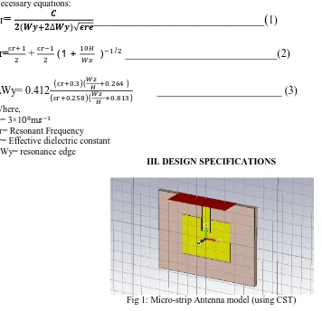
III. DESIGN SPECIFICATIONS
Fig 1: Micro-strip Antenna model (using CST)
E plane is the plane in which the electric filed is dominant and this is validate for H plane too. For example imagine a dipole antenna placed in the X-Y plane (along Y). The E plane is any plane which consists dipole (i.e, YZ or XY) and it’s like an 8. The H plane in this scenario will be orthogonal to dipole antenna (i,e XZ) and the polar pattern will be O shaped [6].
For a linearly-polarized antenna, this is the plane containing the electric field vector and the direction of maximum radiation. The electric field or "E" plane determines the polarization or orientation of the radio wave. For a vertically polarized antenna, the E-plane usually coincides with the vertical/elevation plane. For a horizontally polarized antenna, the E-Plane usually coincides with the horizontal/azimuth plane. E-plane and H-plane should be 90 degrees apart [14]. The E- Plane is any plane that contains the E-field and the direction of maximum radiation from the antenna.
plane usually coincides with the vertical/elevation plane.If the antenna is Micro-strip patch antenna without having slits or slots than it’s very simple to find E-plane and H-Plane [8]. As stated if it’s simple patch antenna than it would be linearly polarized and E-plane would be along the feed line and H-plane would be perpendicular to it [9].
The first step of designing the array is to design the individual element. For this example, a simple square patch antenna was used (Figure 1), and was created directly in CST STUDIO SUITE. The patch is created on a double-layered substrate with an air gap, and is placed inside an ABS box. Two parameters need to be optimized: the length of the patch, in order to adjust the resonant frequency of the patch, and the depth of the air gap, in order to increase its bandwidth.
IV. SIMULATION RESULT ANALYSIS
Now for the radiation pattern the antenna shall be simulated only at 2.1GHz, which is the operating frequency for this design of the patch antenna. Here we have a few different specifications than for the S-Parameters, as frequency at 2.1GHz CPW as 70 and giving new values for the Meshing Parameters. In the first step the current distribution along the antenna is being examined as shown in the figures 5.3.
The average current density is shown in different colors. We can see the average current distribution on the surface of the antenna. As we can observe the current is in the range of -18 to -21 on the top edge, it is almost maximum at the center and it is minimum at the edge of the feed.
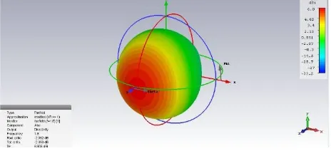
Fig 2: Radiation pattern of Micro-strip patch antenna
Fig 4: Radiation pattern (Kr>>1)
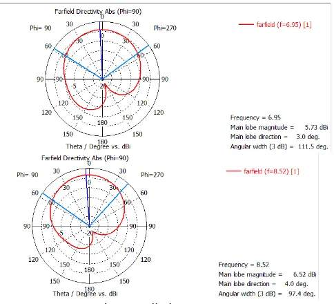
The frequency response of the two-element array is shown in figure (4.5 & 4.6). From these figures we can see that the center frequency of the antenna has changed from 1.8 GHz to 8.52 GHz and the return loss of the antenna increased to -39.1 dB which enhances the total performance of the antenna, while the return loss at 1.2 GHz is -11.4dB.The -10 dB bandwidth is 0.98 GHz begins from 8.1 GHz to 9.08 GHz which is almost the high band frequency of within the region 3 dB.
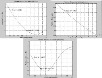
Fig 5: Variation of Radiation Efficiency with Relative Dielectric
Constant for the Micro-strip patch with h=2.88mm and fr= 2GHz.h=2.88mm and fr= 2GHz, with h=2.88mm and r =2.32 [Duroid]
Three variation curves of Radiation pattern graphs are shown upper. There common inputs are: Dielectric Constant of the Patch: 4.5
Upper limit of the resonant frequency : 20×10
Dielectric constant are different in operating frequency usually 2.32 used.
Fig 6: S parameter
Some noteworthy observations are apparent from Figure 4.5. First, the bandwidth of the patch antenna is very small. Rectangular patch antennas are notoriously narrowband; the bandwidth of rectangular micro strip antennas are typically 3%. Secondly, the micro strip antenna was designed to operate at 100 GHz, but it is resonant at approximately 96 GHz this shift is due to fringing fields around the antenna, which makes the patch seem longer. Hence, when designing a patch antenna it is typically trimmed by 2-4% to achieve resonance at the desired frequency. The fringing fields around the antenna can help explain why the micro strip antenna radiates. Consider the side view of a patch antenna, shown in Figure 4. Note that since the current at the end of the patch is zero (open circuit end), the current is maximum at the center of the half-wave patch and (theoretically) zero at the beginning of the patch. This low current value at the feed explains in part why the impedance is high when fed at the end.The designed Micro strip patch antenna with four slits and a pair of truncated corners are simulated using CST for finding the electric far field radiation, gain, directivity, radiation pattern etc. The electric far field of the Micro strip patch antenna is shown in figure 4.5.The gain of the E far field is 270 mv. The operated frequency is 8.52 GHz.
As we see from the graphs, the commercial antennas are the best for checking the results because they have a broad bandwidth and beam width and they are symmetric at 180 degree. So they can capture most frequencies at different orientations.
Ratio of radiated control compactness is specified by bearing to the supremacy thickness of an isotropic orientation transmitter scorching the similar entirety power [4]. The directivity gain of the microstrip patch antenna is 3.1023 dB is shown in Figure 4.6. The competence is distinct as the relation of the radiated power (Pr) to the contribution power (Pi). The contribution power is distorted into exuded power and exterior gesticulate power whereas a minute part is degenerated [5]. The emission prototype is a graphical representation of the comparative pasture potency transmitted as of or conventional. Through the transmitter. Aerial emission patterns are in use at single incidence, on divergence, and one level surface slash. The models are mostly obtainable in glacial or rectilinear appearance by means of a dB potency level The Emission mold is wide elevation
Table 1: Data analysis Table
S S. PM Highest & Lowest power absorption Number of wide-band 1 At 6.9, -16.5 0.23 & 0 1
½ At 7, -18.35 0.37 & 0 1 ¼ At 6.82, -11.6 0.49 & 0.005 1 1/5 At 8.5, -38.9 0.05 & 0.03 3
This table shown variations of power absorption and number of wide band.Main simulation conduct with default value from equations.After that, if i changed its parameter with halved, one-third&one-fifth. It’s clearly shown that if we decrease parameters value up to one-forth highest power absorption will increase but in one-fifth it will decrease. When about low power for if we decrease parameter values we get some value. On the other hand, in one-fifth we got 3 number of wide band. In the process of designing an MPA to perform efficiently, there is always a reflection of the power which leads to the standing waves, which is characterized by the Voltage Standing Wave Ratio (VSWR). As the reflection coefficient ranges from -∞ to 1, the VSWR ranges from 1 to ∞. For the practical applications VSWR = 2 is
acceptable as the return loss would be -9.54dB Return Loss
This is the best and convenient method to calculate the input and output of the signal sources. It can be said that when the load is mismatched the whole power is not delivered to the load there is a return of the power and that is called loss, and this loss that is returned is called the ‘Return loss’.
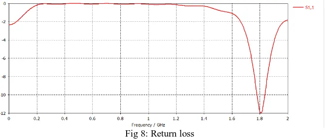
During the process of the design of the rectangular patch antenna there is a response taken from the magnitude of SVs the frequency (this is known as the return loss), as shown in the figure, just as the verification of the design.
Fig 8: Return loss
output power, can be more worse and can become unstable if the VSWR is large. To have a perfect matching between
the antenna and the transmitter, Г=0 and RL = 8, this indicates that there is no power that is returned or reflected but when Г=0 and RL = 0dB, this indicated that the power that is sent is all reflected back.
V. CONCLUSION
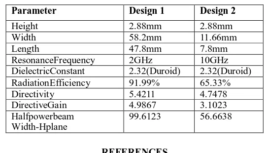
Microstrippatch Antennas were designed in this thesis work according to the requirements of different products. Some products needed a good peak gain and some needed good gain at ±35degree.The first designed antenna was X antenna which was very small in size and still showed good results for all major requirements. Firstly it showed an acceptable r eturn loss around 10 dB, secondly it showed nice gain and thirdly it proved to have an excellent circular polarization. T he major question mark about this antenna is however that it uses a substrate thicknes of 3.2mm which makes it a little expensive, however it is fabricated with a standard FR4 substrate which is significantly cheaper than substrates made es pecially for microwave application. There is a comparison table is given below. Design 2’s parameter is almost half comparing design 1 parameter.
Table 2: Comparison between different design with their response and results
Parameter Design 1 Design 2
Height 2.88mm 2.88mm Width 58.2mm 11.66mm Length 47.8mm 7.8mm ResonanceFrequency 2GHz 10GHz DielectricConstant 2.32(Duroid) 2.32(Duroid) RadiationEfficiency 91.99% 65.33% Directivity 5.4211 4.7478 DirectiveGain 4.9867 3.1023 Halfpowerbeam
Width-Hplane
99.6123 56.6638
REFERENCES
[1] W.C. Weng, F. Yang and A. Elsherbeni, Electromagnetics and Antenna Optimization Using Taguchi's Method, 2007, Morgan&Claypool [2] W.C. Weng, F. Yang and A. Elsherbeni, "Optimization Using Taguchi …",Proc. First European Conference on Antennas and Propagation
[3] W.C. Weng, F. Yang and A. Elsherbeni, "Electromagnetic optimization …",Proc. IEEE APS
[4] W.C. Weng, F. Yang and A. Elsherbeni, "Linear antenna array…", IEEE Trans. Ant. Prop., vol. 55, no. 3, pp. 723-730, 2007 [5] W.C. Weng and T. M. C. Charles, "Optimal Design of CPW …", IEEE Trans. Mag., vol. 45, no. 3, pp. 1543-1545, 2009 [6] W.C. Weng and T. M. C. Charles, "Optimization Comparison between …” Proc. IEEE APS
[7] B. Gökçe and S. Taşgetiren, "KaliteİçinDeneyTasarımı", MakineTeknolojileriElektronikDergisi, vol. 6, no. 1, pp. 71-83, 2009 [8] P.J. Ross, Taguchi Techniques for Quality Engineering, 1996, Mc-Graw-Hill
[9] M. Kara, "The resonant frequency of rectangular …",Microwave Opt TechnolLett, vol. 11, pp. 55-59, 1996
[10]K. R. Carver and J. W. Mink, "Micro strip antenna technology", IEEE Trans. Antennas Propagate., vol. AP-29, no. 1, pp. 2-24, 1981
[11] R. E. Munson, "Conformal micro strip antennas and micro strip phased arrays", IEEE Trans. Antennas Propagate., vol. AP-22, no. 1, pp. 74-77, 1974
[12] A. G. Deanery, Linear micro strip array antennas, 1975
[13] Y. T. Lo, "Theory and experiment on micro strip antennas", IEEE Trans. Antennas Propagate., vol. AP-27, no. 2, pp. 137-145, 1979
[14] P. K. Agrawal and M. C. Bailey, "An analysis technique for micro strip antennas", IEEE Trans. Antennas Propagate., vol. AP-25, pp. 756-758, 1977