ABSTRACT
BAGAL, ABHIJEET SUBHASHRAO. Multifunctional Periodic 3D Thin-shell Nanostructures. (Under the direction of committee chair Dr. Chih-Hao Chang).
The physical properties of naturally occurring bulk materials originate from atomic and molecular arrangements, and are typically coupled. As a result, they lack the ability to have functionalities across multiple domains, their performance being optimized only for one physical domain. Nanomaterials offer unique ability to engineer mechanical, electrical and optical properties independently, making them an attractive candidate for making multifunctional materials.
This work presents a design and fabrication approach to achieve nanostructures with tunable and repeatable multifunctional response. The fabrication approach involves combining nanolithography and atomic layer deposition (ALD) techniques to fabricate thin-shell periodic 3D nanostructures. Use of nanolithography gives precise control over geometrical parameters with nano-meter-level precision, and ALD gives sub-nanometer level control over shell thickness of nanostructures and its material properties. Using this approach, two unique nanomaterials were fabricated over large areas with high spatial coherence, and the method is easily scalable to wafer-size production.
36.3 kJ/kg, surpassing previously reported values at similar densities. The largest length scale in this nanolattice is the 500 nm unit-cell lattice constant, allowing the film to behave more like a continuum material and be visually unobservable. The proposed nanolattice film could find applications in impact mitigation coatings that can be broadly applied over windows, photonic elements, and electronic displays.
Multifunctional Periodic 3D Thin-shell Nanostructures
by
Abhijeet Subhashrao Bagal
A dissertation submitted to the Graduate Faculty of North Carolina State University
in partial fulfillment of the requirements for the degree of
Doctor of Philosophy
Mechanical Engineering
Raleigh, North Carolina 2016
APPROVED BY:
_______________________________ ______________________________ Dr. Gregory Parsons Dr. Christopher Bobko
_______________________________ ______________________________ Dr. Xiaoning Jiang Dr. Yong Zhu
________________________________ Dr. Chih-Hao Chang
DEDICATION
BIOGRAPHY
Abhijeet Bagal is from Latur, a city in Southern Maharashtra. It is located in central India
and has been blessed with a mild weather conducive for learning and education. One of the
most developed cities in Southern Maharashtra; it attracts students from far and wide.
Abhijeet completed Bachelors in Mechanical Engineering in 2005 from SRTMU University
in Latur. His love for scientific enquiry was instrumental in his decision to pursue Masters
from North Carolina in Mechanical and Aerospace Engineering. After completing Masters,
he decided to pursue Doctoral studies in the same group.
ACKNOWLEDGMENTS
I would like to extend my heartfelt gratitude to Dr. Chih-Hao Chang. I will forever be
indebted to him for giving me the opportunity to work in his group. I thank him for imparting
his research skills and for his immense patience when I was learning and failing many times.
His advices have not only helped me greatly in research but have also helped me to be a
better person. I admire his passion for research and teaching, and hope to emulate it. I thank
him for his constant support and encouragement during my doctoral work. Without his expert
guidance and persistent help, this thesis would not have been possible. I thank him for
spoiling me with the best research environment one can ask for, working with him always
felt at home.
I express my gratitude to Dr. Gregory Parsons and Dr. Christopher Bobko for their constant
help and support during my research. Their expert advices have always helped me
immensely. I’m really grateful to Dr. Bobko for his time and effort to teach me
nanoindentation technique and analysis. Special thanks to Dr. Xiaoning Jiang and Dr. Yong
Zhu for serving on my committee, and for providing valuable feedback.
I express my sincere gratitude for the technical support I got from NCSU Nanofabrication
Center and Analytical Instrumentation Facility. I thank Marcio Cerullo, David Vellenga,
Henry Taylor, and Nicole Hedges for training me on various tools and processes in the
cleanroom. Special thanks to Chuck Mooney for training me to use scanning electron
microscope and helping me to take beautiful images of my samples. I have greatly enjoyed
I gratefully thank my lab mates soon-to-be Dr. Xu Zhang (Allan), Jonathan Elek, WeiYi
Chang, Joong-Hee Min, Zhiren Luo, Zhiting Wang, Jared Tippens, Austeen Poteet, Hiro
Nagai, Sharan Naidu, Travis Rivord, Qiaoyin Yang, Chia-Heng Chu, Zhiyuan Xu, and Bin
Dai for their valuable suggestions and helpful discussions. I will dearly miss working with
you all.
Special thanks to my dear friends here in Raleigh and back home in India. I greatly admire
friendship of Arunesh and Aadhithya, they have always supported me and provided useful
advice. I thank Ganesh, Sharavan, Subhash, Srini, Sachin, Nilesh, Akshaya, Prasad, Gerry,
and many more, for their love and support.
I would also like to thank my parents and my sister for all the love and support without which
this thesis would not have been possible. I would like to thank my grandparents Mr. Kisanrao
Deshmukh and Mrs Vimalabai Deshmukh for their love and support. Lastly, I would like to
thank my wife Priyadarshini and her parents Mr. Deepak Padher and Mrs. Shalini Padher for
believing in me, and for being with me through all the ups and downs. Without their help,
TABLE OF CONTENTS
LIST OF TABLES ... x
LIST OF FIGURES ... xi
CHAPTER 1 INTRODUCTION ... 1
1.1 Applications of 3D nanostructures: ... 2
1.1.1 Bioinspired surface functionalities: ... 2
1.1.2 Energy applications:... 5
1.1.3 Mechanical applications: ... 6
1.2 Fabrication approaches to 3D nanostructures: ... 10
1.2.1 Top-down approach: ... 10
1.2.2 Bottom-up approach: ... 16
1.3 Thesis Structure: ... 18
CHAPTER 2 FABRICATION OF LARGE-AREA PERIODIC 3D THIN-SHELL NANOSTRUCTURES ... 20
2.1 Designing of nanolattice material: ... 20
2.2 Approach 1 - interference lithography: ... 26
2.2.1 The Principal of Interference of Light: ... 26
2.2.2 Fabrication of photoresist template using Lloyd’s mirror interferometer: ... 32
2.2.3 Fabrication of thin-shell 1D nano-accordion structure: ... 39
2.2.4 Fabrication of thin-shell 2D nano-pillars: ... 40
2.3 Approach 2 – colloidal phase lithography: ... 49
2.3.1 Talbot effect: ... 49
2.3.3 Fabrication using colloidal phase lithography: ... 52
2.3.4 Fabrication of periodic 3D thin-shell nanolattice film: ... 53
2.4 Summary: ... 59
CHAPTER 3 MECHANICAL TESTING AND ANALYTICAL MODELING OF 3D NANOLATTICE ... 61
3.1 Interference Lithography Stack Design: ... 61
3.1.1 Nanoindentation working principle: ... 61
3.1.2 Methodology to test nanolattice film: ... 64
3.1.3 Methodology to test nanolattice film: ... 66
3.2 Calculation of mechanical properties of nanolattice films: ... 74
3.2.1 Indentation modulus calculation: ... 74
3.2.2 Specific energy dissipation calculation: ... 77
3.2.3 Hardness calculation: ... 80
3.2.4 Failure mode analysis of nanolattice films: ... 82
3.2.5 Elastic recovery of nanolattice films: ... 86
3.2.6 Recoverability analysis of Al2O3 nanolattice when 𝒕 < 𝒕𝒄𝒓:... 90
3.3 Optical properties of nanolattice film: ... 92
3.4 Summary: ... 93
CHAPTER 4 FABRICATION OF 1D NANO-ACCORDION STRUCTURE ... 95
4.1 Need for Stretchable Electronics: ... 95
4.1.1 Nanomaterial-Based Approach: ... 98
4.1.2 Geometry Based Approach: ... 100
4.3 Fabrication Process of Multifunctional Nano-Accordion Structure: ... 103
4.3 Summary: ... 110
CHAPTER 5 MECHANICAL TESTING, NUMERICAL ANALYSIS AND ANALYTICAL MODELING OF 1D NANO-ACCORDIONS ... 111
5.1 Uniaxial Tensile Testing of 1D Nano-accordion: ... 111
5.2 Finite element analysis of 1D nano-accordion structure: ... 119
5.3 Analytical Modeling of 1D nano-accordion structure: ... 130
5.3.1 Strain in ZnO-PDMS composite section: ... 130
5.3.2 Strain in curved section: ... 131
5.3.3 Deflection of vertical section: ... 133
5.4 Compression Induced Breaking of Nano-accordion Structure: ... 138
5.5 Tensile Loading Induced Systematic Failure of Nano-accordion Structure: ... 141
5.6 Summary: ... 142
CHAPTER 6 ELECTRICAL AND OPTICAL CHARACTERIZATION OF 1D NANO-ACCORDIONS ... 144
6.1 Electrical characterization of nano-accordions: ... 144
6.2 Optical characterization of nano-accordions: ... 157
6.3 Summary: ... 163
CHAPTER 7 CONCLUSION ... 166
REFERENCES ... 170
APPENDICES ... 188
PHOTORESIST BURN-OFF CHARACTERIZATION USING DIFFERENTIAL SCANNING CALORIMETRY ... 189 COURTESY OF ED MILY AND DR. J. P. MARIA, DEPARTMENT OF
MATERIALS SCIENCE AND ENGINEERING, NCSU ... 189 APPENDIX B ... 191 ATOMIC LAYER DEPOSITION (ALD) RECIPES ... 191 COURTESY OF ERINN DANDLEY, DR. JUNJIE ZHO, DR. CHRISTOPHER
OLDHAM AND PROF. GREGORY PARSONS, DEPARTMENT OF CHEMICAL AND BIOMOLECULAR ENGINEERING, NCSU ... 191 APPENDIX C ... 193 OPTICAL SIMULATION OF NANO-ACCORDION STRUCTURE ... 193 COURTESY OF XU A. ZHANG, DEPARTMENT OF MECHANICAL AND
LIST OF TABLES
Table 3-1: Loads used in cyclic incremental loading of nanolattice films ... 68
Table 3-2: Mechanical properties of nanolattice ... 82
Table 3-3: Elastic recovery of Al2O3 nanolattice films ... 88
Table 5-1: Stress-strain values for experimentally tested nano-accordion samples ... 126
LIST OF FIGURES
Figure 1-1: (a) Antireflective nanostructure of moth eye.2 (b) High-aspect nanocone
structures. (c) Multifunctionalities of nanostructured glass.7 ... 3
Figure 1-2: (a) Hierarchical structure on gecko feet.8 (b, c) Directional dry adhesive with hierarchical nanostructures.9,10 (d) Directional wetting of butterfly wings.1 (e) Directional wetting achieved with asymmetric nanostructured surface.11 ... 5
Figure 1-3: (a) 3D nano-pillar array photovoltaic.12 (b) SEM of NKN nano-rod array for piezoelectric energy harvesting.14 (c) 3D bicontinuous battery electrodes and SEM.15 ... 6
Figure 1-4: (a) Bone showing microscale random arrangement of constituent elements.21 (b) Polymer foam with random structure. 25 Scale bar is 1 μm ... 8
Figure 1-5: (a) Solid alumina microlattice fabricated by microstereolithography.39 (b) Hollow alumina nanolattice fabricated with two photon lithography.36 ... 9
Figure 1-6: (a) Optical setup for two photon lithography.45 (b) Spiral structure made by two photon lithography. (c) Complex 3D structure made by two photon lithography.46 ... 12
Figure 1-7: Multibeam interference lithography. 47 ... 13
Figure 1-8: 3D nanostructure fabrication using phase shift mask.48 Images in red box are micrographs of various geometries created using phase mask. Simulated intensity pattern is also show in the inset.49 ... 15
Figure 1-9: (a) 3D nanostructure by block copolymer assembly.50 (b) 3D nanostructure by self-assembly of colloidal particles.51 ... 17
Figure 2-1: Unit cell geometries for bulk, solid core and hollow core structures... 21
Figure 2-2: Axial loading condition. ... 22
Figure 2-3: Bending loading condition. ... 23
Figure 2-4: Diagram of the proposed fabrication process. (a) Solid polymer structure fabricated using 3D nanolithography. (b) Thin layers of metal oxides are coated using ALD. (c) Remove polymer to form a hollow-core oxide tubular nanolattice. ... 26
Figure 2-5: Periodicity of interference pattern ... 30
Figure 2-7: SEM’s of Periodic nanostructures fabricated using Lloyd’s mirror
interferometer. (a) 1D nanostructure with 500 nm period. (b) 1D nanostructure with 200 nm period. (c) 2D nanostructure with 500 nm period. (d) 2D nanostructure with 200 nm period. ... 34 Figure 2-8: Schematic of ILIL setup with Lloyd’s mirror interferometer in a fluid medium with high refractive index (n > 1).18 ... 36 Figure 2-9: Top view micrographs for fabrication results obtained using ILIL setup at = 325 nm for (a)-(c) DI water (n = 1.33)and (d)-(f) immersion oil (n = 1.51) at various incident angles. Grating structures patterned in DI water with (a) 170 nm period at θ = 46º, (b) 160 nm period at θ = 49.8º, and (c) 150 nm period at θ = 54.5º. Grating structures patterned in immersion oil with (d) 140 nm period at θ = 50.5º, (e) 130 nm period at θ = 56º, and (f) 120 nmperiod at θ = 64.5º. ... 37 Figure 2-10: Schematic of proposed ILIL setup with Lloyd’s mirror interferometer in a fluid medium with high refractive index (n > 1).18 ... 38 Figure 2-11: Period reduction with use the of immersion fluid. Continuous lines show
numerical model of grating period (Λ) as a function of angle of incidence (𝜃) for = 325 nm. The discrete points are experimental results for respective immersion media.18 ... 39 Figure 2-12: SEM’s of Periodic nanostructures fabricated using Lloyd’s mirror
Figure 2-15: SEM’s after burn-off of 2D 500 nm period photoresist sample coated with 30 nm Al2O3 at 550°C for 30 minutes with 5°C/min ramp rate. (a) SEM showing the
Figure 2-22: Scanning electron micrographs of samples used for mechanical testing. (a-b) Cross-sectional image of ZnO nanolattices with thicknesses 45 nm and 75.5 nm respectively. (c-d) Cross-sectional image of Al2O3 nanolattices with thicknesses 30 nm, 20 nm, 15 nm, and 6 nm respectively. (f) Top-view SEM of 15 nm Al2O3 nanolattice ... 57 Figure 2-23: 10 nm ZnO nanolattice. (a) Top view SEM showing cracks in the nanolattice after removing resist template. (b) Cross-sectional SEM showing structure collapses readily due to cracks. ... 58 Figure 3-1: Geometry of contact with spherical indenter. (a) Schematic showing loading of a preformed impression of radius 𝑅𝑟 with a spherical rigid indenter of radius 𝑅𝑖. (b) Load-displacement curve for an elastic-plastic specimen. 76,77 ... 63 Figure 3-2: Load-displacement curve showing elastic and plastic work of indentation 76,77 . 64 Figure 3-3: CSM UNHT nanoindenter. ... 65 Figure 3-4: Top-view SEM of nanoindentation area for 30 nm ZnO sample. ... 66 Figure 3-5: Mechanical testing of nanolattice using nanoindentation. (a) Schematic of
Figure 3-8: Modulus scaling for nanolattice film. The relative moduli of Al2O3 and ZnO nanolattice plotted against relative density for all the tested samples. The results for both ALD materials follow power law with scaling n ~ 1.1. ... 76 Figure 3-10: Hysteresis loops for 4 nm Al2O3 nanolattice... 79 Figure 3-11: Specific energy dissipation scaling for nanolattice film. Specific energy
dissipation for Al2O3 and ZnO nanolattice plotted against relative density. The Al2O3
nanolattice shows more favorable power law scaling... 80 Figure 3-12: Hardness scaling for nanolattice film. Pop-in hardness versus relative density. The nanolattice shows similar hardness scaling for both Al2O3 and ZnO. ... 81 Figure 3-13: Failure mode analysis of Al2O3 nanolattice. ... 84 Figure 3-14: Failure mode analysis of ZnO nanolattice. ... 85 Figure 3-15: Elastic recovery of Al2O3 nanolattice films. Elastic recovery of Al2O3
nanolattice film plotted as a function of relative density and nanolattice shell thickness. Error bars represent standard deviation in elastic recovery. ... 87 Figure 3-16: (a) Elastic recovery vs. force. (b) Elastic recovery vs. displacement ... 89 Figure 3-17: Optical image of 10 nm Al2O3 sample and bare glass. “Nano” is the Al2O3 nanolattice film with 10 nm shell thickness. A phone screen was used as backlit background. Scale bar is 1 cm. ... 92 Figure 4-1: (a) Flexible display by SONY. (b) Rollable 18 inch OLED display by LG. (c) Transparent display by LG. (d) Conformable epidermal electronics on human skin which can be compressed and stretched.91 (e) Wearable sensor on human skin.103 ... 97 Figure 4-2: (a) Stretchable conductor using ITO on PDMS.20 (b) Graphene based flexible conductors with serpentine interconnects.4 (c) CNT based flexible conductor.16 (d) Ag
Figure 5-2 SEM tensile test stage with 30 nm nano-accordion sample at 0% strain. Red arrows indicate the direction of stretching. ... 113 Figure 5-3 Stretching mechanism for the nano-accordion structure. SEM images show the 30 nm thick ZnO nano-accordion structure being stretched under tensile loading. The 10 period marker is defined by the white arrows, indicating period increase with increasing strain. No systematic failure can be observed up to 51% strain. ... 114 Figure 5-4 Tensile loading tests to study effect of nano-accordion height on its stretchability. Each column shows the top-view SEM’s of corresponding nano-accordion sample with gradual increase in strain ... 115 Figure 5-5 Top view SEM images at failure strain with nano-accordion height change. For all the nano-accordion samples, the thickness of ZnO layer is 30 nm. (a) h = 1100 nm, 𝜖𝑚𝑎𝑥
= 53% (b) h = 850 nm, 𝜖𝑚𝑎𝑥 = 34% (c) h = 735 nm, 𝜖𝑚𝑎𝑥 = 26% (d) h = 570 nm, 𝜖𝑚𝑎𝑥 = 18% ... 116 Figure 5-8 Cross-sectional SEM of ZnO nano-accordion with h = 1100 nm, 𝑡𝑧 = 30 nm, and
𝛬 = 500 nm. ... 119 Figure 5-9 Simplified accordion geometry in ANSYS. Both PDMS and ZnO nano-accordion are meshed using mapped face meshing. Nano-nano-accordion mesh is further refined to get smoother stress profile. Contact region is created at the interface between PDMS and ZnO nano-accordion. ... 121 Figure 5-10 Finite element analysis of 1D nano-accordion structure (a) FEA model showing highest stress in the inner curved section of nano-accordion geometry under tensile loading. Failure stress (red) is about 760 MPa for a sample with h = 1100 nm, 𝑡𝑧 = 30 nm, 𝛬 = 500 nm, and 𝑟2 = 115 nm. (b) FEA model showing highest stress in the ZnO-PDMS composite region. ... 123 Figure 5-11 Comparison of strain contribution by individual elements of nano-accordion Strain contribution by individual elements of nano-accordion with h = 1100 nm, 𝑡𝑧 = 30 nm,
Figure 5-12 Comparison of stress in curved section and ZnO-PDMS composite section of nano-accordion Stress contribution is plotted for nano-accordion with h = 1100 nm, 𝑡𝑧 = 30 nm, 𝛬 = 500 nm, and 𝑟2 = 115 nm. Stress in curved section is higher than stress in
ZnO-PDMS composite and ZnO vertical section at all strain values. ... 125
Figure 5-13 Effect of nano-accordion thickness on local maximum stress. Simulated maximum stress versus strain curve for a 30 nm thick ZnO nano-accordion structure with different heights. The failure strains obtained experimentally are plotted to determine corresponding local failure stress, which has an average value of 800 MPa. ... 127
Figure 5-14 Effect of nano-accordion thickness on local maximum stress. Simulated stress vs strain curve for h = 1100 nm and 𝛬 = 500 nm, with different thicknesses. Experimental results for failure strain are plotted on respective curves to get corresponding local stress. Black dotted line indicates averaged failure stress, which is about 800 MPa. ... 128
Figure 5-15 Division of one period of nano-accordion geometry in three parts ... 130
Figure 5-16 ZnO-PDMS composite section under tensile loading ... 131
Figure 5-17 Curved section of nano-accordion under tensile loading ... 132
Figure 5-18 Deflection of vertical section of nano-accordion under loading ... 133
Figure 5-19 Comparison of stretchability versus nano-accordion height using the analytical model, FEA, and experimental data. ... 136
Figure 5-20 Comparison of stretchability versus normalized geometric parameter ℎ3/𝑡 using the analytical model, FEA, and experimental data. ... 137
PDMS and ZnO. The schematic shows the forces acting on sample during tensile loading
test. ... 140
Figure 5-22 Tensile loading induced failure. Top-view SEM image of 30 nm nano-accordion sample with h = 1100 nm, showing systematic failure of nano-accordion structure due to tensile loading. Failure due to compressive loading is also shown in the figure. ... 141
Figure 6-1 ZnO doping mechanism ... 145
Figure 6-2 Custom-built stage for stretching and bending tests of nano-accordion ... 148
Figure 6-3 Custom-built stage for stretching and bending tests of nano-accordion ... 148
Figure 6-4 (a) Relative resistance versus strain in static loading. (b-c) optical images show the AZO nano-accordion sample as a stretchable transparent conductor at 0% and ~30% strain. Scale bars, 1 cm (b, c). ... 150
Figure 6-5 Relative resistance versus strain with intermediate load-unload cycles for 50 nm AZO nano-accordion ... 151
Figure 6-6 Cyclic tensile loading-unloading performance of 50 nm AZO nano-accordion at 20% strain ... 152
Figure 6-7 Cyclic tensile loading-unloading performance of 50 nm AZO nano-accordion at 30% strain ... 153
Figure 6-8 (a) Relative resistance versus bending radius. (b, c) Optical images show electrical performance for bending. Scale bars, 1 cm (b, c). ... 154
Figure 6-9 Cyclic tensile loading-unloading performance of 50 nm AZO nano-accordion 155 Figure 6-10 (a) Relative resistance versus bending radius. (b) Schematic of bending mechanism ... 156
Figure 6-11 Broadband optical transmittance spectra of planar 30 nm AZO film on glass slide ... 157
birefringence along fold direction of nano-accordion geometry. (d) Diffraction and light trapping effect of nano-accordion structure. Optical image of 50 nm AZO nano-accordion structure on PDMS under normal incidence of white light. Bright orange color at the edge of PDMS is due to diffracted orders trapped in PDMS. (e) Total, specular and diffused
Chapter 1 Introduction
These advancements have enabled rigorous understanding of micro/nanostructure enabled biological multifunctionalities, and help pave ways to functional mimicry of these natural designs.
Many bioinspired applications and fabrication approaches involving nanostructures in zero dimension (0D), one dimension (1D), two dimensions (2D) and three dimensions (3D) have been explored. Due to the vast scope of this field, in this chapter I will focus extensively on the applications and fabrications techniques of 3D nanostructures. Functional enhancements using 3D nanostructures have been achieved in wide variety of area. A brief overview of their bioinspired surface functionalities and applications in energy and mechanics will be presented. Mechanical applications and principle governing mechanical performance will be discussed extensively as this forms core of this work. A brief review of 3D manufacturing techniques will also be provided.
1.1Applications of 3D nanostructures: 1.1.1 Bioinspired surface functionalities:
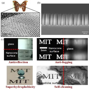
micro/nanoscale features on these surfaces has enhanced their functionalities beyond their constituent materials. Such multifunctional nanocone structures have been realized using lithography and etching techniques. They have also demonstrated that by having ordered, densely-packed, high-aspect ratio nanocone structure further enhances the functionalities.7 As shown in Figure 1-1 (b, c), the nanocone structured glass shows enhanced optical transmission, self-cleaning, superhydrophobicity and, anti-fogging properties.
Figure 1-2: (a) Hierarchical structure on gecko feet.8 (b, c) Directional dry adhesive with hierarchical nanostructures.9,10 (d) Directional wetting of butterfly
wings.1 (e) Directional wetting achieved with asymmetric nanostructured surface.11
1.1.2 Energy applications:
supercapacitor-like charge-discharge rate capability and battery-like large storage capacities.
Figure 1-3: (a) 3D nano-pillar array photovoltaic.12 (b) SEM of NKN nano-rod array for piezoelectric energy harvesting.14 (c) 3D bicontinuous battery electrodes and
SEM.15
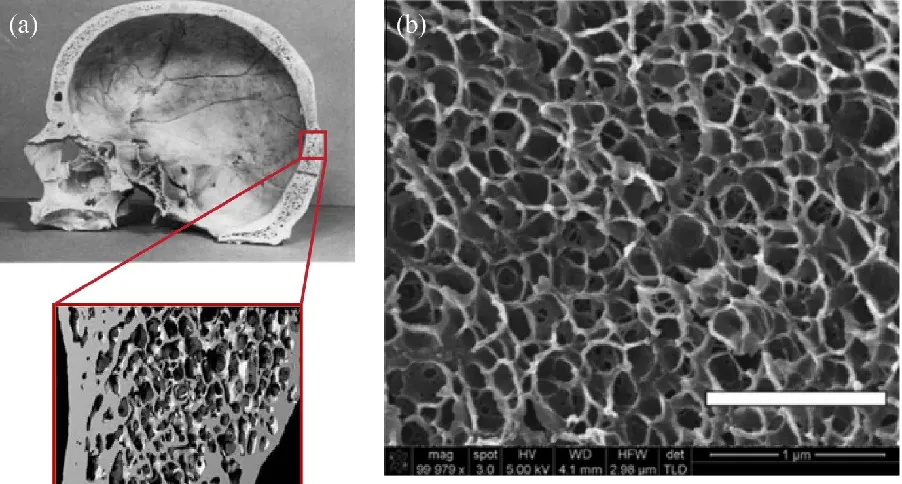
1.1.3 Mechanical applications:
Figure 1-4: (a) Bone showing microscale random arrangement of constituent elements.21 (b) Polymer foam with random structure. 25 Scale bar is 1 μm
material response can be better tailored to achieve optimal mechanical response. Figure 1-5 shows ordered 3D microstructures with optimized mechanical properties.
Figure 1-5: (a) Solid alumina microlattice fabricated by microstereolithography.39 (b) Hollow alumina nanolattice fabricated with two photon lithography.36
novel nanomechanics, the nanolattices coverage area are generally limited to 100×100 m2 range and implementation over large area remains a significant challenge.
1.2 Fabrication approaches to 3D nanostructures:
Various approaches to fabricating 3D nanostructures have been demonstrated with abilities to fabricate geometries of varying complexities. The choice of approach mainly depends on materials to be processed, desired nanostructure configuration, complexity of the technique and processing cost. These approaches have broadly been categorized in two types as ‘top-down’ and ‘bottom-up’ approach. The top-down approach to nanofabrication generally involves creating nanostructures by breaking down larger materials through physical and/or chemical processing. Examples of top-down approach are; lithography techniques (photon, electron-beam, focused ion beam, soft, immersion, nano imprint, etc.), etching techniques (wet and dry), electrospinning, mechanochemical bonding and milling. The bottom-up approach to nanofabrication involves atom-by-atom, molecule-by-molecule, or nanoparticle self-assembly to make nanostructures. Examples of bottom-up approach are; vapor-phase techniques (atomic layer deposition, epitaxy, etc.), liquid-phase techniques (electrodeposition, Sol-gel) and self-assembly techniques. In the next section I will briefly discuss few of these approaches used for making 3D nanostructures.
1.2.1 Top-down approach:
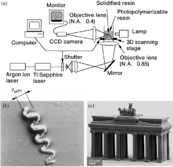
Figure 1-6: (a) Optical setup for two photon lithography.45 (b) Spiral structure made by two photon lithography. (c) Complex 3D structure made by two photon
lithography.46
TM components of the beam, necessitating the mechanism for correction. For this, an appropriately shaped refractive index matched prisms is used, but every new structural geometry requires a specially designed prism, making it very design and cost intensive process. Fabrication area depends on the overlay region of beams, and expanding the beam to achieve large area fabrication will be difficult as it will lead to non-uniformities in beam intensity.
Figure 1-7: Multibeam interference lithography. 47
Figure 1-8: 3D nanostructure fabrication using phase shift mask.48 Images in red box are micrographs of various geometries created using phase mask. Simulated
intensity pattern is also show in the inset.49
industry have invested heavily to keep up with the Moor’s law, but many believe that we will reach the physical limit for the resolution that can be achieved using top-down approach. The next approach discussed presents a promising way to overcome this challenge.
1.2.2 Bottom-up approach:
Researchers have always been intrigued by the way nature assembles basic building blocks to make DNA’s and RNA’s, and have been working on developing techniques to achieve similar feat. 3D nanostructures fabricated with the self-assembly of block copolymers and colloidal particles have been demonstrated.49, 50 In recent years block copolymer self-assembly has gained lot of attention as it offers size and shape tunability at nanoscale by changing their molecular weights and compositions. Variety of shapes have been fabricated using self-assembly of block copolymers.50 An ordered 3D nanostructure fabricated using block copolymer assembly is shown in Figure 1-9 (a). The main challenge for this approach lies in the control of microstructure geometry. To achieve a high quality structure with precise microdomain location, orientation, and elimination of various defects requires introduction of external fields during the processing step.50
fabricate nanostructures over large areas. But challenge still lies in the ability to precisely control the arrangement of colloidal particles to achieve desired geometries, and random nature of the process results in grain boundaries and point defects within the structure.
Figure 1-9: (a) 3D nanostructure by block copolymer assembly.50 (b) 3D nanostructure by self-assembly of colloidal particles.51
1.3 Thesis Structure:
In this chapter, I briefly introduced the application of 3D nanostructures and various fabrication techniques used to achieve them. This work is focused on systematic design and fabrication of ordered 3D nanostructures to achieve functionalities in multiple domains, with primary focus on their mechanical properties.
In chapter 2, I will discuss the relationship between relative modulus and relative density for cellular materials, which governs their mechanical properties and plays important role in material selection. A design philosophy for the architectural arrangement of constituent elements of cellular materials will be discussed. Based on this design philosophy, two fabrication approaches combining nanolithography and atomic layer deposition (ALD) technique to fabricate large-area ordered 3D nanomaterials will be presented. The first approach demonstrates the fabrication of a thin-shell nanomaterial with accordion-fold, bend-dominated architectural arrangement. More details on the mechanical, electrical and optical characterization of this nanomaterial, with application for making stretchable transparent conductor will be presented in Chapter 4-6. The second fabrication approach demonstrates the fabrication of a thin-shell 3D nanolattice film with stretch-dominated architectural arrangement. Such structural arrangement enhances the mechanical properties of the nanomaterial and is ideal for making lightweight, ultrastrong materials.
energy dissipation and hardness will be calculated and analyzed with respect to nanolattice density. A recoverability analysis of Al2O3 nanolattices will be presented. An analytical model describing the failure mode mechanism of nanolattices will be presented. This analytical model helps to understand the complete recoverability demonstrated by Al2O3 nanolattices.
In Chapter 4, initially a detailed background on need for flexible electronics and various approaches used to achieve those will be presented. Later, I will present a modified version of the first fabrication approach to achieve stretchable transparent conductors using 1D nano-accordion geometry. This approach will enable precise design of individual geometrical parameters of the nano-accordion and helps to achieve predictable mechanical, electrical and optical performance.
In Chapter 5, I will present a methodology used for tensile testing of 1D nano-accordions. Experimental analysis of the effect of geometrical parameters on the stretchability of nano-accordions will be discussed in detail. A finite element analysis model used to understand the stress behavior and failure mode of nano-accordion will be presented. Later, an analytical model relating the stretchability of nano-accordions to its geometrical parameters and material properties will also be presented.
Chapter 2 Fabrication of Large-area Periodic 3D
Thin-shell Nanostructures
In this chapter will cover two approaches I developed to fabricate periodic complex 3D thin-shell nanolattice material. These approaches involve combining nanolithography and ALD to achieve precise control over the geometry and material properties of the fabricated nanomaterial. Areas in excess of few square centimeters can be fabricated using both approaches and are easily scalable for wafer-level fabrication. The initial section of this chapter will present the designing of optimum geometry of nanolattice material and the technical approach used to fabricate nanolattice material. Later, a detailed description of the two fabrication approaches will be provided.
2.1 Designing of nanolattice material:
2.1.1 Scaling factors under mechanical loading:
The scaling factor between Young’s modulus (E) and density (𝜌) obeys power law (𝐸 ∝ 𝜌𝑛)21,53, and the unit cell geometry of the material plays an important role in determining this scaling factor (n). Three unit-cell geometries (size 𝐷 × 𝐷) are considered to find the relative scaling factor between Young’s modulus and density. These three unit cells represent bulk material, solid-core architectural element and hollow-core structural architectural element respectively. Analysis of these unit cells will help to understand the difference between mechanical properties of bulk material and cellular material with solid-core and hollow-solid-core architectural elements. The parameters 𝑑𝑜 and 𝑑𝑖 are the outside and inside diameters as shown in Figure 2-1.
Figure 2-1: Unit cell geometries for bulk, solid core and hollow core structures.
The density (𝜌) of each unit cell is a function of material mass (m) enclosed in the unit cell and the volume (V) of the unit cell.
𝜌 = 𝑚 𝑉⁄
Where 𝜌𝑚 is the density of material, and A is the cross-sectional area of the region covered by material in the unit cell. For simplicity, the unit-cell volume (V) and its length (L) are assumed to be same in all three cases. This leads to dependence of density for bulk (𝜌𝑏), solid core (𝜌𝑠𝑐), and hollow core (𝜌ℎ𝑐) unit cells, on their respective cross-sectional areas. The cross-sectional areas for bulk, solid core and hollow core unit cells are 𝐴𝑏= 𝐷2 ,
𝐴𝑠𝑐 = 𝜋𝑑𝑜2/4 ,and 𝐴
ℎ𝑐 = 𝜋𝑑𝑖𝑡/2 respectively.
The relative density scales by a factor of 2 with respect to its geometry.
𝜌𝑠𝑐
𝜌𝑏 𝛼 ( 𝑑02
𝐷2)
𝜌ℎ𝑐 𝜌𝑏 𝛼 (
𝑑𝑖𝑡 𝐷2)
Under axial loading conditions, the resistance to deformation is defined by the stiffness of the material (K).54
𝐾 =𝐸𝐴
𝐿
Figure 2-2: Axial loading condition.
As both Young’s modulus (E) and length (L) are constant, same as in case of density, the relative stiffness too scales with a factor of 2 to its geometry.
𝐾𝑠𝑐
𝐾𝑏 = 𝜋𝑑𝑜2
𝐾ℎ𝑐 𝐾𝑏 =
𝜋𝑑𝑖𝑡 2𝐷2
This gives a linear relationship between relative stiffness and density as below;
𝐾𝑠𝑐 𝐾𝑏 𝛼
𝜌𝑠𝑐
𝜌𝑏 (2.1)
𝐾ℎ𝑐 𝐾𝑏 𝛼
𝜌ℎ𝑐
𝜌𝑏 (2.2)
This result shows that the relative modulus for structures under axial loading scales with a power of 1, which is linear scaling, with respect to relative density. Note this compares with scaling factor of 3-4 for random structures. Therefore structures with architectural elements aligned along the loading direction are ideal for compressive and tensile loading conditions.
Beyond axial loading, the effect of bending on density scaling is also important. Resistance to bending is characterized by the flexural rigidity (R) of the beam.54
𝑅 = 𝐸𝐼
Where, 𝐼 is the second moment of inertia. The moment of inertia for square bulk, solid core and hollow core are 𝐼𝑏 = 𝐷4/4, 𝐼𝑠𝑐 = 𝜋𝑑𝑜4/64, and 𝐼𝑠𝑐= 𝜋𝑑𝑖3𝑡/8, respectively. The relative flexural rigidities are then,
𝑅𝑠𝑐 𝑅𝑏 =
𝑑04
16𝐷4 𝑅ℎ𝑐 𝑅𝑏 = 3𝜋 2 ( 𝑑𝑖 𝑡) ( 𝑑𝑖𝑡 𝐷2)
2
This results in;
𝑅𝑠𝑐 𝑅𝑏 𝛼 ( 𝜌𝑠𝑐 𝜌𝑏) 2 (2.3) 𝑅ℎ𝑐 𝑅𝑏 𝛼 ( 𝜌ℎ𝑐 𝜌𝑏) 2 (2.4)
This result shows that, the relative modulus for structures under bending scales with a power of 2 with respect to relative density. Note this is worse than axial loading, but is better than random architectures. Such structures will be inherently weaker but have shown remarkable recoverability from compressive loading.34,36,44
2.1.2 Technical approach:
Figure 2-4: Diagram of the proposed fabrication process. (a) Solid polymer structure fabricated using 3D nanolithography. (b) Thin layers of metal oxides are coated using
ALD. (c) Remove polymer to form a hollow-core oxide tubular nanolattice.
This approach to nanolattice fabrication gives ability to deterministically design the lattice constants during nanolithography, and control shell thickness and material properties during ALD process. Use of ALD process provides a wide range of oxides and metals (Al2O3, ZnO, TiO2, W, Pt, etc.) that can be used for conformal coating. The following sections will present the two approaches explored to fabricate large area periodic 3D thin-shell nanomaterials.
2.2 Approach 1 - interference lithography:
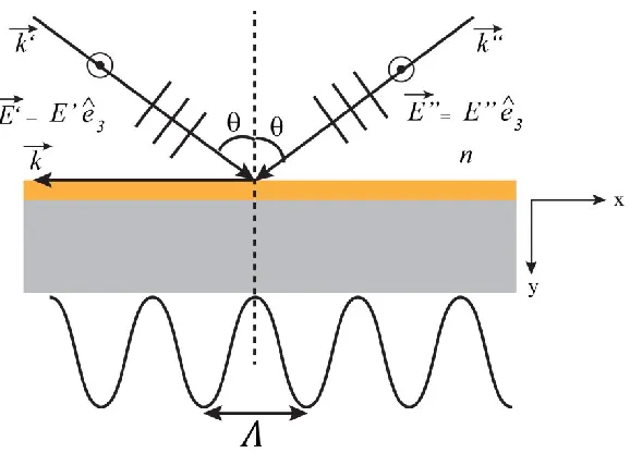
In this section, background information on interference of light will be provided, followed by fabrication process for making periodic photoresist templates using Lloyd’s mirror interferometer.
2.2.1 The Principal of Interference of Light:
field 𝐸⃗ and the magnetic field 𝐻⃗⃗ . For a light wave propagating through a source free, linear, isotropic and homogenous region, the electric and magnetic fields are inter-related through the Maxwell’s equations. In Maxwell’s equations, both these fields are function of position r and time t.59–61
∇ × E⃗⃗ (r , t) = −μ∂H⃗⃗ (r , t)
∂t (2.5)
∇ × H⃗⃗ (r , t) = ε ∂E⃗⃗ (r , t)
∂t (2.6)
∇ · E⃗⃗ (r , t) = 0 (2.7)
∇ · H⃗⃗ (r , t) = 0 (2.8)
Where, μ is permeability and ε is permittivity of the medium through which light propagates. The electric and magnetic fields from Maxwell’s curl equations can be separated to form a wave equation;
∇2𝐸⃗ − 1
𝑐2
𝜕2𝐸⃗
𝜕𝑡2 = 0 (2.9)
∇2𝐻⃗⃗ − 1
𝑐2
𝜕2𝐻⃗⃗
𝜕𝑡2 = 0 (2.10)
Where, c is the speed of light.
𝛹 = 𝐴𝑒𝑗(𝜔𝑡−𝒌⃗⃗ .𝒓⃗ )
(2.11) The electric and magnetic fields can be found using complex function formulation;
𝐸⃗ (𝑟 , 𝑡) = 𝐸˳𝑒(−𝑗(𝑘⃗ .𝑟 −𝜔𝑡)
(2.12) Where, E0 is the magnitudes of electric and magnetic field respectively, ω is the angular velocity of the wave, k is the wave vector and its magnitude in terms of wavelength λ, is given by;
∣ 𝑘⃗ ∣ = 𝑘 = 2𝜋
𝜆 (2.13)
In case of interference lithography, the exposure dose required to get the desired pattern in the photoresist is critical quantity. Exposure dose represents the amount of energy received by photoresist per unit area per unit time. This quantity is known as optical intensity or irradiance and is given by following equation;
𝐼 = 𝜀𝜐 < 𝐸⃗ 2 >
𝑇 (2.14)
𝐼 ≈< 𝐸⃗ 2 >
𝑇= < 𝐸⃗ · 𝐸⃗ ∗ >𝑇 (2.15)
We are interested in the phenomenon in which two coherent plane waves are added together such that the resultant wave has either greater or lower amplitude. This is known as interference. Consider two waves of the form;
𝐸′
⃗⃗⃗⃗ (𝑟 , 𝑡) = 𝐴′𝑒(−𝑗(𝑘⃗⃗⃗⃗ .𝑟 −𝜔𝑡) ′ (2.16)
𝐸"
⃗⃗⃗⃗ (𝑟 , 𝑡) = 𝐴"𝑒(−𝑗(𝑘⃗⃗⃗⃗ .𝑟 −𝜔𝑡+Δϕ) "
(2.17) These two waves interfere with each other to form an interference pattern.
𝐼 = |𝐸⃗ ′+ 𝐸⃗ "|2
𝐼 = (𝐸⃗ ′+ 𝐸⃗ ")(𝐸⃗ ′∗+ 𝐸⃗ "∗)
𝐼 = 𝐼′+ 𝐼"+ [( 𝐸⃗ ′. 𝐸⃗ "∗) + (𝐸⃗ ′∗. 𝐸⃗ ")]
𝐼 = 𝐼′+ 𝐼"+ 2(𝐸⃗ ′· 𝐸⃗ ")cos [(𝑘⃗ ′− 𝑘⃗ ") · 𝑟 + Δϕ]
(2.18) Equation (2.14) gives the total irradiance due to two interfering waves. It is difficult to measure the electric field, so for exposure dose intensity of incident light is measured. By using only the magnitudes of electric field, we get;
Figure 2-5: Periodicity of interference pattern
The two plane waves represented by equation (2.12) and (2.13) interfere with each other to give a sinusoidal intensity pattern. The maxima and minima of this sinusoidal intensity pattern are known as interference fringes. We are interested in finding the periodicity of these fringes as these will define the period of the structure that we get using interference lithography. The fringe vector is given by;
𝑘⃗ = 𝑘⃗ ′− 𝑘⃗ " = 𝑘
𝑥𝑒̂1+ 𝑘𝑦𝑒̂2+ 𝑘𝑧𝑒̂3 (2.20) Assume the spatial vector 𝑟 is parallel to the fringe vector 𝑘⃗ , also 𝑟 and 𝑘⃗ are along x-axis. The spatial phase then can be written as a product of magnitude of fringe vector and the spatial position.
𝛿 = |𝑘⃗ |𝑟
𝛬 =2𝜋
𝑘⃗ (2.21)
For two beams drawn from a single monochromatic source of light, magnitude of wave vector is same i.e. |𝑘⃗ ′| = |𝑘⃗ "|. The individual vector components along unit axis are related as; 𝑘"
𝑒1 = −𝑘′1𝑒1 , 𝑘′1𝑒2 = 𝑘"𝑒2 , 𝑘′1𝑒3 = 𝑘"𝑒3. Substituting this in equation 2.16, we get;
𝑘⃗ = 2𝑘"
𝑒2𝑒̂2 (2.22)
Using this result and with equations (2.9) and (2.17), we get the following relation for periodicity of fringes;
𝛬 = 𝜆|𝑘"|
2𝑘2𝑒2 (2.23)
From figure 2-1, we can define the relationship between angle of incidence one of the wave vector.
𝑠𝑖𝑛𝜃 = 𝑘
" 𝑒2
|𝑘⃗ "|
So the periodicity of the two interfering beams is given by equation (2.20) and this identity is valid only when the only when the angle bisector of two interfering beams is normal to the direction of fringe period.
𝛬 = 𝜆
2.2.2 Fabrication of photoresist template using Lloyd’s mirror interferometer:
Figure 2-6: Lloyd’s mirror interferometer
Figure 2-7: SEM’s of Periodic nanostructures fabricated using Lloyd’s mirror interferometer. (a) 1D nanostructure with 500 nm period. (b) 1D nanostructure with 200 nm period. (c) 2D nanostructure with 500 nm period. (d) 2D nanostructure with 200 nm
period.
Figure 2-8: Schematic of ILIL setup with Lloyd’s mirror interferometer in a fluid medium with high refractive index (n > 1).18
Figure 2-9: Top view micrographs for fabrication results obtained using ILIL setup at = 325 nm for (a)-(c) DI water (n = 1.33)and (d)-(f) immersion oil (n = 1.51) at various incident angles. Grating structures patterned in DI water with (a) 170 nm period at θ = 46º, (b) 160 nm period at θ = 49.8º, and (c) 150 nm period at θ = 54.5º.
Grating structures patterned in immersion oil with (d) 140 nm period at θ = 50.5º, (e) 130 nm period at θ = 56º, and (f) 120 nmperiod at θ = 64.5º.
Figure 2-10: Schematic of proposed ILIL setup with Lloyd’s mirror interferometer in a fluid medium with high refractive index (n > 1).18
Figure 2-11: Period reduction with use the of immersion fluid. Continuous lines show numerical model of grating period (Λ) as a function of angle of incidence (𝜃)
for = 325 nm. The discrete points are experimental results for respective immersion media.18
2.2.3 Fabrication of thin-shell 1D nano-accordion structure:
20-30 minutes in solvent. The superior mechanical properties of Al2O3 ensure that the ALD layer does not collapse during solvent dissolution process and maintains its shape to achieve accordion-fold geometry.
Figure 2-12: SEM’s of Periodic nanostructures fabricated using Lloyd’s mirror interferometer. (a) 1D nanostructure with 500 nm period. (b) 1D nanostructure with 200 nm period. (c) 2D nanostructure with 500 nm period. (d) 2D nanostructure with 200 nm
period.
This accordion-fold nanostructure is demonstrated to make stretchable transparent conductors. More details on the fabrication process and characterization are presented in Chapter 4-6.
2.2.4 Fabrication of thin-shell 2D nano-pillars:
The 2D nano pillar fabricated using Lloyd’s mirror interferometer can also be coated conformally with oxide/metal layer using ALD. The solvent dissolution method used for
removing the 1D photoresist templates will not be useful for removing 2D photoresist templates,
new method of burning-off the photoresist at elevated temperatures to make the isolated
structures hollow. The initial trial involved heating the sample in a furnace (Vulcan 3 series) at
750°C for 30 minutes with 5°C/min ramp rate. The initial results after burn-off of a sample with
30 nm ZnO layer on a 500 nm period 2D photoresist templet are shown in Figure 2-13.
The ZnO layer deposited during ALD is polycrystalline with the grain size 12 ± 4 nm. During burning process, the photoresist and ARC burns-off and the vapors created escape
through the gaps between adjacent grains, leaving behind hollow nano-pillars as shown in Figure
2-13. Inset in Figure 2-13 (c) shows the top view SEM of the sample before burning photoresist.
As seen from the SEM’s after burning, during the template removal process, diameter of the
hollow ZnO pillar shrinks by ~30% and holes are developed in the structure. This results from
the high temperature ramp rate and high temperature used for the process, making burning
Figure 2-13: SEM’s after burn-off of photoresist at 750°C for 30 minutes with 5°C/min ramp rate. (a-c) cross-sectional SEM’s pf the sample. A 500 nm 2D photoresist sample coated with 30 nm ZnO was used. Inset in (c) shows the top-view
SEM of the sample before thermal treatment.
The initial results from this experiment showed that using thermal treatment it is possible
reducing the temperature ramp rate to 0.3°C/min and trying different temperatures between 500 -
750°C, with a step of 50°C. Figure 2-14 shows the cross-sectional SEM images of a sample after
thermal treatment at 550°C. From SEM’s it can be observed that the 2D pillars are hollow-core
with a ZnO shell thickness of 30 nm. Also, it is clear that there is no shrinkage or formation of
holes in the nano-pillars during template removal process. This results from the slower ramp rate
used for thermal treatment. The photoresists completely burns-off at about 550°C, and this result
Figure 2-14: SEM’s after burn-off of photoresist at 550°C for 30 minutes with 0.3°C/min ramp rate. (a-c) cross-sectional SEM’s pf the sample. A 500 nm 2D photoresist sample coated with 30 nm ZnO was used. Inset in (c) shows the top-view
Figure 2-15: SEM’s after burn-off of 2D 500 nm period photoresist sample coated with 30 nm Al2O3 at 550°C for 30 minutes with 5°C/min ramp rate. (a) SEM showing the delamination of Al2O3 film during thermal treatment. (b) Exploded nano-pillars during thermal treatment. Delamination’s and explosions were observed
at only few locations. (c) SEM showing good region on sample without any damage to nano-pillars during thermal treatment. (d) Nano-pillars dislodged by scratching the sample. Nano-pillars are hollow after thermal treatment and are undamaged after
dislodging.
Figure 2-16: Schematic of bubbles created by thermal treatment of nano-pillars coated with ALD layer. Red arrows indicate the pressure exerted on the walls
2.3 Approach 2 – colloidal phase lithography:
Beyond free-space laser interference lithography, interactions between colloidal particles and light can also be used for nanolithography. I used the complex 3D periodic photoresist templates fabricated using colloidal phase lithography52,67 developed in our research group. In this approach, 2D close-packed array of polystyrene particles is assembled on a photoresist surface end illuminated with a light source. The resulting optical intensity pattern is governed by the Talbot effect in the near field, and is recorded by photoresist. Post-exposure developing of the photoresist results in complex 3D periodic nanostructure. Similar to earlier approach, the photoresist templates fabricated by this method can be coated conformally with oxide/metal layers using ALD, and later the photoresist was removed to achieve free-standing 3D thin-shell nanolattices. Compared to earlier approach to lithography, this approach does not require any specialized hardware and provides a low-cost, rapid, and easily scalable approach to fabricate nanostructures over large areas. But challenge still lies in the ability to precisely control the arrangement of colloidal particles to achieve desired geometries, and random nature of the process results in grain boundaries and point defects within the structure.
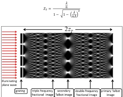
2.3.1 Talbot effect:
structure in subsequent planes.70–72 When a plane wave transmits through periodic diffraction gratings, the image of the grating gets repeated at regular distances away from the grating plane. This regular distance is called Talbot length (𝑍𝑇), and the repeated images are called Talbot images, shown in Figure 2-17. The Tablot length is the function of wavelength (𝜆) of light used, period of diffraction grating (𝛬) and refractive index of the propagating medium (𝑛), and is given by48,68,69;
𝑍𝑇 =
𝜆 𝑛
1 − √1 − (𝑛𝛬)𝜆 2
Figure 2-17: Optical Talbot effect for monochromatic light72
fabrication of high-quality mold for PDMS replication. The process to make mold typically requires use of expensive and time-consuming fabrication processes such as deep UV, electron-beam, or atomic force lithography followed by plasma dry etching. The approach developed by our lab is simple, cost effective and scalable. It involves using colloidal polystyrene spheres as phase elements to achieve Talbot effect.
2.3.2 Self-assembly of colloidal particles:
Figure 2-18: Steps involved in colloidal self-assembly at air/water interface and subsequent transfer of colloidal monolayer transfer on substrates.73
2.3.3 Fabrication using colloidal phase lithography:
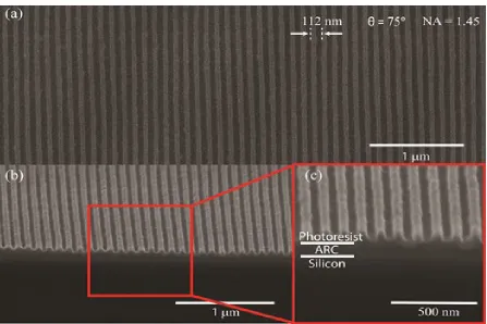
Figure 2-19: Three-dimensional nanolithography using colloidal particle phase masks. (a) Fabrication principles. (b) SEM images of fabricated 3D nanostructures.52
2.3.4 Fabrication of periodic 3D thin-shell nanolattice film:
Figure 2-20: Fabrication process of ordered 3D nanolattice thin-film. (a) A 3D photoresist template was fabricated using colloidal phase lithography. SEM image
shows ordered 3D photoresist structure (D = 500 nm, λ = 325 nm). (b) Photoresist template was conformally coated using atomic layer deposition technique. SEM
image shows 40 nm Al2O3 conformally coated on photoresist template. (c) Photoresist template removal to achieve hollow shellular 3D nanolattice film. SEM
shows a free-standing 3D nanolattice with 40 nm shell thickness.
particle diameter (D = 500 nm) ratio, which governs the unit-cell geometry.67 After removing the sacrificial polymer template, the resulting structure has a unique arrangement of tubular thin-shell elements, which imparts enhanced mechanical stability to the nanolattice film under normal compressive loading. This is analogous to micron-scale structural anisotropy obtained through processing in Damascus steel to achieve better strength and toughness.75 This lithography configuration was used to fabricate all the samples.
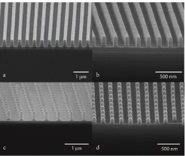
Figure 2-21: Scanning electron micrographs of samples used for mechanical testing. (a-c) Cross-sectional image of ZnO nanolattices with thicknesses 95 nm, 58 nm, and
45 nm respectively. (d-f) Cross-sectional SEM image of Al2O3 nanolattices with thicknesses 19 nm, 10 nm, and 4 nm respectively. The thinnest nanolattice tested for
mechanical properties had a shell thickness of 4 nm. Cross-sectional image of 4 nm nanolattice shows the structure is free-standing and does not collapse during
template removal process.
Figure 2-22: Scanning electron micrographs of samples used for mechanical testing. (a-b) Cross-sectional image of ZnO nanolattices with thicknesses 45 nm and 75.5 nm respectively. (c-d) Cross-sectional image of Al2O3 nanolattices with thicknesses
Figure 2-22 shows the cross-sectional micrographs of remaining nanolattice samples tested for mechanical properties. All the samples have architectural arrangement consisting of primary hollow tubular columns surrounded by secondary thin-shell structures. The secondary shell structure helps to further enhance the robustness of the nanolattice.
ZnO nanolattices with shell thickness smaller than 30 nm were difficult to fabricate, as the structure collapses during the template removal process. Figure 2-23 shows the top view and cross-sectional SEM image of 10 nm ZnO nanolattice after removing the resist template. The porous morphology is due to the polycrystalline nature of ALD coated ZnO.
Figure 2-23: 10 nm ZnO nanolattice. (a) Top view SEM showing cracks in the nanolattice after removing resist template. (b) Cross-sectional SEM showing
2.4 Summary:
In this chapter initially I presented a design philosophy to optimize the performance of ordered nanostructures. The stretch dominated structures are desirable for applications requiring high strength to weight ratio of the structures. The arrangement of constituent elements along the direction of external load (tensile or compressive) helps to improve its load bearing capacity. For such structures, the relative stiffness scales linearly with the relative density. Bending dominated structures are inherently weaker, and for these structures relative stiffness scales with a power of 2 with respect to relative density. Such structures are good for applications requiring high deformations, stretchability and recoverability of structure.
Later, I presented two fabrication approaches to make submicron-scale ordered thin-shell 3D nanostructures over a large area. The first approach involved patterning photoresist template using interference lithography, followed by subsequent coating of photoresist template and template removal to achieve free-standing hollow structure. Using this approach two novel geometries were presented. Application of 1D nano-accordion geometry to make stretchable transparent conductors will be presented Chapter 4-6. Initial fabrication results for 2D thin-shell nano-pillars achieved by thermal treatment to remove photoresist were also demonstrated. The unique geometry and large area fabrication of this structure makes it an attractive candidate for many applications discussed. This structure is part of future study.
makes it an ideal candidate for applications involving loads normal to the surface. A detailed analysis of mechanical properties of this structure will be presented in Chapter 3.
Chapter 3 Mechanical Testing and Analytical Modeling of
3D Nanolattice
In Chapter 2, I presented two approaches combining nanolithography and ALD to fabricate ordered 3D thin-shell nanostructures with complex geometries. Both of these approaches present ways to make ordered nanomaterials with sub-micron lattice constants over large areas. In this chapter, I will present the methodology used for mechanical testing of 3D nanolattice using nanoindentation technique, followed by analysis of the data collected. Analytical model to understand the failure mode mechanism of the 3D nanolattice will also be presented.
3.1 Interference Lithography Stack Design:
The mechanical properties of thin-shell 3D nanolattice films fabricated using the technique discussed in last chapter were tested using nanoindentation technique. This section will discuss the nanoindentation principle, tool and methodology used.
3.1.1 Nanoindentation working principle:
predetermined load is applied to the specimen through a diamond indenter of desired geometry (spherical, conical, Barkovich, flat punch, etc.), actuated through a piezoelectric mechanism to achieve precise loading. Figure 3-1 (a) shows the schematic of spherical indenter on a specimen.77 A peak indentation load (𝑃𝑚𝑎𝑥) is applied to the specimen through a spherical indenter of radius (𝑅𝑖), and the corresponding displacement of the indenter is recorded continuously. A typical load-displacement curve showing loading-unloading cycle is shown in Figure 3-1 (b). When the specimen is loaded, the initial response is elastic followed by elastic-plastic deformation. At peak indentation load, the depth of indentation beneath the original specimen surface is ℎ𝑚𝑎𝑥, but the actual contact depth is ℎ𝑐. When the load is removed, the specimen recovers through height ℎ𝑒 and at complete unload, there is a residual imprint of depth ℎ𝑟. The contact depth ℎ𝑐 is the distance from the contact circle to the bottom of indenter contact as shown. The radius of contact circle a is related to indenter load, radius, and modulus of contacting materials through76,77;
𝑎 = 3𝑃𝑅𝑖 4𝐸∗
𝐸∗ is the reduced modulus and is related to the modulus of indenter and specimen through76,77;
𝐸∗ = (1 − 𝜈2)
𝐸 +
(1 − 𝜈𝑖2)
𝐸𝑖
Figure 3-1: Geometry of contact with spherical indenter. (a) Schematic showing loading of a preformed impression of radius 𝑅𝑟 with a spherical rigid indenter of
radius 𝑅𝑖. (b) Load-displacement curve for an elastic-plastic specimen. 76,77
The nanoindenter is mostly used to determine the modulus and hardness of the specimen. The modulus is related to the slope S of unloading curve through following equation76,77;
𝐼𝑛𝑑𝑒𝑛𝑡𝑎𝑡𝑖𝑜𝑛 𝑚𝑢𝑑𝑢𝑙𝑢𝑠 = 𝑆√𝜋 2𝛽√𝐴
Where β is the correction factor based on geometry on indenter and A is the contact area given by76,77;
𝐴 = 𝜋(2𝑅𝑖ℎ𝑐− ℎ𝑐2) = 2𝜋𝑅 𝑖ℎ𝑐
loading-unloading curve is the plastic work (𝑊𝑝𝑙𝑎𝑠𝑡𝑖𝑐) and signifies the energy absorbed during indentation. This is illustrated in Figure 3-2.
𝑊𝑝𝑙𝑎𝑠𝑡𝑖𝑐 = 𝑊𝑡𝑜𝑡𝑎𝑙 − 𝑊𝑒𝑙𝑎𝑠𝑡𝑖𝑐
Figure 3-2: Load-displacement curve showing elastic and plastic work of indentation 76,77
3.1.2 Methodology to test nanolattice film:
Figure 3-3: CSM UNHT nanoindenter.
result in at least one ‘pop-in’ (first occurrence of mechanical failure within nanolattice) event during loading. On remaining nanolattice samples, larger area was marked for nanoindentation and the small indents were made at 35 locations to collect more data for analysis of mechanical properties.
Figure 3-4: Top-view SEM of nanoindentation area for 30 nm ZnO sample.
3.1.3 Methodology to test nanolattice film:
Table 3-1: Loads used in cyclic incremental loading of nanolattice films Shell
thickness (nm)
Incremental loads (µN)
1 2 3 4 5 6 7 8 9 10
Al2 O3
40 50 90 157 349 635 963 1366 1837 2383 3000 30 50 70 137 267 437 654 920 1231 1592 2000
20 50 60 79 108 159 227 295 383 486 600
15 50 54 68 90 120 158 206 262 328 400
10 25 27 33 44 60 79 103 131 164 200
6 25 26 28 33 40 49 48 71 84 100
4 10 16 21 27 32 38 43 49 55 60
Z
n
O
95 50 90 157 349 635 963 1366 1837 2383 3000
75.5 50 68 120 222 341 499 698 930 1199 1500
58 50 62 83 122 168 251 331 438 566 700
45 50 64 93 143 219 313 428 567 722 900
30 50 57 73 100 139 190 251 323 399 500
reliable data for mechanical properties, each nanolattice sample was tested at multiple locations.
Figure 3-5: Mechanical testing of nanolattice using nanoindentation. (a) Schematic of nanoindentation mechanism. (b) Typical cyclic load-displacement curve for 30
nm Al2O3 nanolattice. ‘Pop-in’ indicates first instance of mechanical failure of nanolattice film. Inset shows post-indent SEM image with residual indentation imprint, showing brittle fracture of top planar layer. The top planar layer cracks around holes indicating stress concentration under compressive loading. (c)
Load-displacement curve for 4 nm Al2O3 nanolattice showing gradual ‘pop-in’ event. Inset shows post-indent SEM with no residual indentation imprint. Adhesion force results from the van der Waal’s attraction between Al2O3 nanolattice and diamond indent. Non-zero adhesion force indicates complete recovery of nanolattice post indentation. (d) Load-displacement curve for 45 nm ZnO nanolattice showing
‘pop-in’ event similar to thicker Al2O3 nanolattice. Inset shows post indent SEM image with brittle fracture around holes.
Figure 3-6: Load-displacement curves (a - d) load-displacement curves for 15 nm, 20 nm, 10 nm and 6 nm Al2O3 nanolattices respectively. (e, f) load-displacement
The nanolattices have few imperfections arising from particle assembly defects during the self-assembly step. To ensure the data collected during nanoindentation was from defect-free regions, post indent SEM images of all the samples were taken. Figure 3-7 shows the load-displacement curve for a 45 nm ZnO nanolattice when the indent was made on a defect. Due to the presence of the defect, the structure collapsed during loading. Due to structure collapse, a dramatic increase in displacement was recorded at lower loads. Inset shows SEM with indentation residue on a defect. Only the nanoindentation data collected from defect-free regions were considered for calculating mechanical properties of the nanolattice. All the samples studied in this work were tested at 30 different locations. Out of these tests, about 15-25% were rejected due to the indents made on grain boundaries or point defects.