Characterisation of Self
Assembled Nanostructures
Lina Persechini
School of Physics
Trinity College Dublin, Ireland
A thesis submitted for the degree of
Philosophiæ Doctor (PhD)
Declaration
This thesis has been submitted to the University of Dublin for examination for
the degree of Doctor in Philosophy by the undersigned.
This thesis has not been submitted as an exercise for a degree to any other
uni-versity.
With the exception of the assistance noted in the acknowledgments, this thesis is
entirely my own work.
I agree that the Library of the University of Dublin may lend or copy this thesis
upon request.
Lina Persechini October 2012
School of Physics,
University of Dublin,
The use of optical techniques for material characterisation offer several
advan-tages: it is non–destructive, useful in all pressure ranges, and a wide range of
material systems can be probed. However, it is not always possible to isolate the
surface or interface contribution. Epioptics refers to a special branch of optics
devoted to the measurement of the surface and interface responses. Reflection
anisotropy spectroscopy (RAS) and Second–harmonic generation (SHG) studies were carried out on various self–assembled systems including: self–assembled
plas-monic nanostructures and ultra–thin chiral films. These very different systems
will show how useful these techniques are for material growth and charcterisation.
RAS is very useful to grow and tune plasmonic nanostructures for a wide
range of applications. SHG is a nonlinear technique which is sensitive to localised
surface plasmon resonances (LSPRs), and consequently weak nonlinear signals are
amplified. SHG was used to charcterise silver on rippled silicon templates, where
interesting information can be extracted on the symmetry and morphology of the
nanoparticle (NP) layer.
Modelling these plasmonic resonances is often challenging and complex espe-cially when dealing with arbitrary shapes. The linear optical response of these
structures was modelled with a view to enable the responses of any plasmonic
structure using any template to be predicted.
Chiral molecules are by nature asymmetric. SHG is highly symmetry
depen-dent, and so was used to detect ultra–thin films of a chiral molecule (cysteine) in
Contents
Declaration i
Abstract i
Acknowledgments iii
List of publications vi
List of figures xi
List of tables xii
List of abbreviations xii
1 Introduction 1
1.1 Surface and interface optics . . . 1
1.1.1 Reflection anisotropy spectroscopy . . . 5
1.1.2 Second–harmonic generation . . . 6
1.2 Plasmonic nanostructures . . . 8
1.2.1 Overview of the literature . . . 8
1.2.1.1 Optical techniques . . . 13
1.3 Thin film chiral systems . . . 15
1.3.1 Overview of the literature . . . 16
1.3.1.1 Optical techniques . . . 17
2.1.1 Reflection anisotropy spectroscopy . . . 24
2.1.1.1 Origin of a RAS signal . . . 26
2.1.2 Spectroscopic ellipsometry . . . 28
2.2 Nonlinear optical response of materials . . . 31
2.2.1 Second–harmonic generation . . . 31
2.2.1.1 Phenomenological model . . . 34
2.2.2 Investigation of chirality using SHG . . . 37
2.2.2.1 Phenomenological model . . . 38
3 Experimental techniques and procedures 42 3.1 Ultra high vacuum (UHV) . . . 43
3.2 Sample preparation . . . 44
3.2.1 Rippled silicon templates . . . 44
3.2.2 Preparation of chiral binol samples . . . 47
3.2.3 Preparation of chiral cysteine films . . . 48
3.3 Reflection anisotropy spectroscopy . . . 51
3.3.1 Introduction . . . 51
3.3.2 Experimental arrangement . . . 51
3.4 Second–harmonic generation . . . 55
3.4.1 Introduction . . . 55
3.4.2 Experimental arrangement . . . 55
3.5 Conventional surface science techniques . . . 59
3.5.1 Low energy electron diffraction (LEED) . . . 59
3.5.2 Auger electron spectroscopy (AES) . . . 60
3.6 Spectroscopic ellipsometry . . . 62
4 Analytic theory of the linear optical response of aligned ellip-soidal nanoparticles on planar surfaces 65 4.1 Theory and phenomenological model . . . 66
4.1.1 Dielectric function of the NP material . . . 68
4.1.2 Isolated NP and local field effects . . . 71
4.1.2.1 Size effects . . . 72
4.1.2.2 Capping effects . . . 72
CONTENTS
4.1.4 Retardation effects . . . 77
4.1.5 Solving the T–matrix . . . 80
4.2 Pb on Si(557)–Au . . . 81
4.2.1 Ag on Al2O3 . . . 81
4.2.2 Ag on rippled Si(001) . . . 84
4.3 Conclusions . . . 87
5 Linear and nonlinear characterisation of plasmonic nanostruc-tures on rippled Si templates 88 5.1 Rippled Si templates . . . 89
5.1.1 Ambient measurements . . . 89
5.1.1.1 RAS . . . 91
5.1.1.2 SHG . . . 93
5.1.2 In situ measurements . . . 98
5.1.2.1 RAS . . . 100
5.1.2.2 SHG . . . 100
5.2 Plasmonic structures . . . 103
5.2.1 Ag on rippled Si templates . . . 103
5.2.1.1 RAS . . . 104
5.2.1.2 SHG . . . 108
5.2.2 Ag on Al2O3 . . . 113
5.2.2.1 SHG . . . 113
5.3 Conclusions . . . 116
6 Optical characterisation of small organic chiral molecules at sur-faces 119 6.1 Ultra–thin binol films on fused silica . . . 120
6.2 Cysteine on reflecting surfaces . . . 127
6.2.1 Cysteine on Si(001) . . . 127
6.2.2 Cysteine on Au(110) . . . 131
6.2.3 RAS response of cysteine on Au(110) . . . 133
6.2.4 SHG response of cysteine on Au(110) . . . 138
7 Conclusions and future work 145
List of publications
Persechini, L. & McGilp, J. F. Chiral second-harmonic generation from small
organic molecules at surfaces. Physica status solidi (b), 2012.
Persechini, L. and Ranjan, M. and Grossmann, F. and Facsko, S. and McGilp,
J. F. The linear and nonlinear optical response of native-oxide covered rippled Si
1.1 A comparison of escape depth between optical and electron based
techniques . . . 3
1.2 Epioptics . . . 3
1.3 Metallic sphere in an EM field . . . 9
1.4 Applications of plasmonic structures. . . 10
1.5 Colloidal nanoparticles . . . 11
1.6 Cysteine pairs observed by STM. . . 11
1.7 Examples of templates for the production of aligned arrays. . . 12
1.8 Chirality. . . 17
1.9 Cysteine pairs observed by STM. . . 18
1.10 Acridine substituted Tr¨oger base. . . 20
2.1 Principle of RAS. . . 26
2.2 Comparison of RAS response from Si(100) and Au(110) . . . 27
2.3 The principle of ellipsometry . . . 29
2.4 Reflection of s and p light from a surface. . . 30
2.5 SHG geometry in reflection from a surface. . . 36
2.6 Optical activity of a helical molecule . . . 39
3.1 Schematic cross-section of the vacuum system . . . 44
3.2 Sample holder used for preparing rippled Si in UHV. . . 45
3.3 Ion gun used to make rippled samples. . . 46
3.4 AFM of a rippled Si sample template. . . 47
3.5 2-D schematic of R– and S–binol . . . 47
LIST OF FIGURES
3.7 Sample Holder for Au(110) . . . 49
3.8 Sample Holder for Au(110) . . . 50
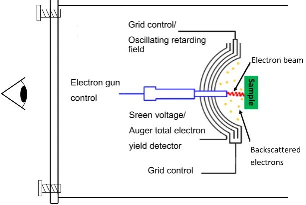
3.9 Diagram of a PEM RAS setup . . . 52
3.10 Photo of smaller RAS and Broad band RAS . . . 53
3.11 Schematic of the rotating polariser SHG experimental arrangement. 58 3.12 LEED image of the Au(110)–1×2 reconstruction. . . 60
3.13 Schematic of the LEED-Auger system . . . 61
3.14 Schematic of the Auger effect. . . 61
3.15 AES spectra from clean Si and Au substrates . . . 62
3.16 Schematic of ellipsometry system. . . 63
4.1 Experimental RAS data from uncapped Pb islands. . . 68
4.2 Experimental RAS data from capped Pb islands. . . 69
4.3 RAS spectra showing the effect of changing the island length. . . 73
4.4 RAS spectra showing the effect of changing the island width. . . . 74
4.5 RAS spectra showing the effect of capping the nanosructures. . . 74
4.6 RAS showing the effect of including dipole–dipole effects from neighbouring islands in thex direction. . . 76
4.7 RAS spectra showing the effect of including dipole–dipole effects from neighbouring islands in the y direction. . . 77
4.8 RAS . . . 78
4.9 RAS spectra showing the effect of including the MLWA correction. 79 4.10 RAS . . . 82
4.11 RAS . . . 82
4.12 RAS . . . 83
4.13 RAS . . . 84
4.14 RAS . . . 85
4.15 SEM of Ag deposited on rippled Si. . . 86
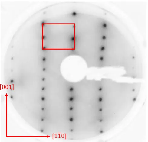
4.16 Simulated RAS spectra of Ag on rippled substrate. . . 86
5.1 Cross–sectionalTEM image of rippled Si(001). . . 90
5.2 RAS response of rippled templates. . . 92
5.5 α–s response from rippled samples. . . 96
5.6 α–s response from rippled samples. . . 96
5.7 α–p response from rippled samples. . . 97
5.8 AFM of rippled sample grown in UHV. . . 99
5.9 RAS response of rippled templates with increasing irradiation. . . 101
5.10 RAS response of rippled substrate measured in ambient. . . 102
5.11 α–p response from UHV grown rippled samples. . . 102
5.12 Cross–sectional TEM image of silver NPs on a rippled Si substrate. 104 5.13 SEM imagesof Ag cluster samples. . . 106
5.14 RAS response of capped Ag NPs on rippled substrates. . . 107
5.15 RAS response from Ag on rippled Si without a capping layer. . . . 107
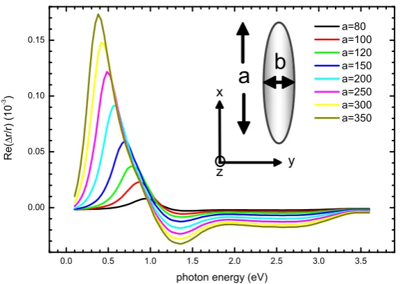
5.16 Geometry of SHG meaurements. . . 109
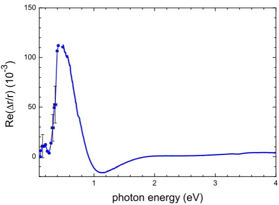
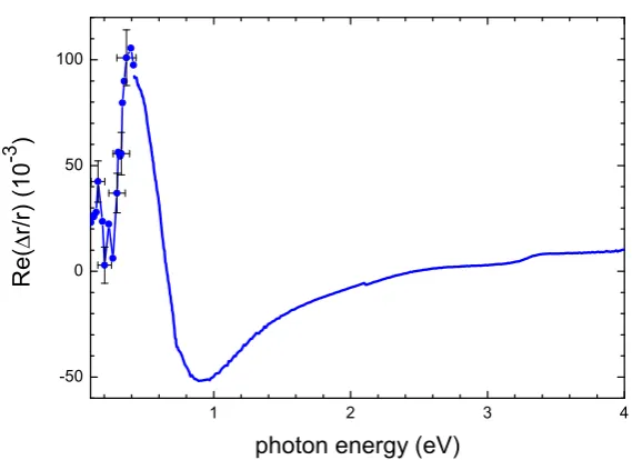
5.17 α–p response of capped Ag on rippled Si substrates. . . 112
5.18 α–s response of the capped Ag on rippled Si substrates. . . 112
5.19 α–p response of Ag on facetted sapphire. . . 115
5.20 α–s response of Ag on facetted sapphire. . . 115
5.21 α–p response of Ag on a flat sapphire substrate. . . 116
5.22 α–s response of Ag on a flat alumina substrate. . . 116
6.1 Chiral SHG setup for reflection and transmission studies . . . 121
6.2 SHG response of (R)– and (S)–binol . . . 123
6.3 Binol geometry . . . 124
6.4 SHG response of Racemic binol . . . 126
6.5 Resonantly enhanced chiral effects from binol . . . 126
6.6 Model of cysteine . . . 127
6.7 SHG response of native–oxide covered Si(001). . . 129
6.8 SHG response of ultra–thin films of (R)– and (S)–cysteine . . . . 130
6.9 (S)–(-)–cysteine on Au(110)–2×1 surface. . . 132
6.10 RAS response of (R)–(+)–cysteine . . . 134
6.11 RAS response of (S)–(−)–cysteine . . . 134
6.12 RAS spectra taken in transient . . . 135
LIST OF FIGURES
6.14 LEED images taken of (R)– and (S)–cysteine compared with clean
Au(110). . . 137
6.15 line scan . . . 138
6.16 SHG response of clean Au(110) . . . 141
2.1 Non zeroχ(2) components. . . . 33
2.2 Independent components of tensors χeee, χeem and χmee. . . . . . 40
4.1 Material parameters for bulk Ag and Pb. . . 70
5.1 Sample details of capped and uncapped Ag islands. . . 105
5.2 Fitted parameter values and allowed tensor for Ag on rippled Si. . 110
5.3 Fitted parameter values and allowed tensor for Ag on rippled Si. . 111
5.4 Fitted parameter values and allowed tensor for Ag on Al2O3. . . . 114
5.5 Fitted parameter values and allowed tensor for Ag on Al2O3. . . . 114
6.1 Fitted parameter values and allowed tensor for (R)–binol on fused silica . . . 122
6.2 Fitted parameter values and allowed tensor for (S)–binol on fused silica . . . 123
6.3 Fitted parameter values and allowed tensor for racemic–binol on fused silica . . . 125
6.4 Fitted parameter values and allowed tensor for clean Si(001) . . . 128
6.5 Fitted parameter values and allowed tensor for (R)–(+)–cysteine on Si(001) . . . 129
6.6 Fitted parameter values and allowed tensor for clean Au(110) . . 140
List of abbreviations
AES Auger electron spectroscopy
AFM Atomic force microscopy
aSi Amorphous silicon
BBO Beta barium borate
CD Circular dichroism
Binol 1,1’–binaphthalene–2,2’– diol
D Dextrorotatory
IR Infrared
L Levorotatory
LDA Local density approximation
LEED Low energy electron diffraction
LN Liquid nitrogen
LPR Localised surface plasmon resonance
ML Monolayer
MOKE Magentic optical Kerr effect
NP Nanoparticle
PEM Photo-elastic modulator
PMT Photo muliplier tube
List of Abbreviations
SEM Scanning electron microscopy
SHG Second harmonic generation
SP Surface plasmon
STM Scanning tunneling microscopy
UHV Ultra high vacuum
Introduction
“Begin at the beginning,” the
King said, gravely, “and go on
till you come to the end; then
stop.”
–Lewis Carroll, Alice in Wonderland
This chapter introduces the field of epioptics, which is a specialised area of
optical techniques devoted to surface and interface characterisation. The material
systems studied in this thesis, including plasmonic structures and thin film chiral
systems, will be introduced. An overview of the literature is also provided,
high-lighting the advantage of using epioptic techniques to characterise these systems.
1.1
Surface and interface optics
When optical radiation is used to probe a material, it has the ability to penetrate
1.1 Surface and interface optics
surface contribution difficult. However, the surface or interface structure differs
significantly from that of the bulk. The optical techniques have been developed
which exploit these differences, and measure the optical response of the surface
or interface with sub–ML resolution. Figure 1.1 compares sampling depths for
electrons to those of photon–based techniques. For metals optical radiation
pene-trates∼10 nm, which allows buried interfaces to be probed. Since the first optics
experiment by Chiarottiet al in 1968 [1], which identified the presence of surface
states on the cleaved (111) surface of Ge, many more experimental techniques
have been developed [2] in order to understand condensed matter surfaces and
interfaces. In particular, the exploitation of symmetry differences between the
bulk and the surface has led to the development of a unique area of optics for
surface and interface characterisation termed “epioptics” (from the Greek “epi”
meaning upon) [3].
In general, optical techniques offer significant advantages over traditional
elec-tron based techniques. Optical techniques are non–invasive and non–destructive,
all pressure ranges are accessible allowingin situ monitoring of monolayer growth.
The characterisation of a wide range of material systems (such as liquid–solid,
liquid–liquid and solid–solid interfaces) is possible due to the penetration depth
of the radiation.
The interaction of an electromagnetic (EM) field of frequency ω with matter induces a polarisation which can be described as an expansion.
P(ω,2ω) =0[χ(1)(ω)E(ω) +χ(2)(ω,2ω)E2(ω) +....] (1.1)
ma-Figure 1.1: A comparison of escape depth between optical and electron based techniques
Optical characterisation of plasmonic structures
incident photons
surface
reflected photons
second-harmonic photons
scattered photons (Raman)
cap buried interface
(nanostructure)
[image:19.595.145.498.167.403.2]substrate cap
1.1 Surface and interface optics
terial response. The first term on the right–hand side of Equation 1.1 describes
the linear optical response, which is exploited in techniques such as
spectro-scopic ellipsometry (SE) and reflection anisotropy spectroscopy (RAS). In
lin-ear optics the dielectric tensor, (ω), is related to the linear susceptibility by
(ω) = 1 +χ(1)(ω). However, the nonlinear term in Equation 1.1, which depends
on χ(2)(ω,2ω), becomes significant at high EM field strengths and has a
polar-isation quadratic in the EM field. χ(2)(ω) describes the lowest–order nonlinear
optical response responsible for second–harmonic generation (SHG). Higher order
terms are also possible within the electric dipole approximation: in the absence of
any resonantly enhanced surface electric dipole effects, the third–order response
χ(2)(ω,2ω,3ω) probes the bulk, while fourth–order terms are surface sensitive but
require compressed pulses of high peak power in order to observe them.
Sym-metry arguements have been used to show that the rank of the tensor and the
order of the multipole expansion of the EM field determine the degree of the
surface and interface rotational anisotropy that can be probed [4]. Within the
electric dipole approximation, an nth rank tensor can exhibit up to n–fold ro-tational anisotropies. Therefore experimental techniques based on different rank
tensors will provide complementary information. RAS, for example, can detect
two–fold in plane rotational anisotropy, while SHG can detect up to three–fold
anisotropy and in principle fourth–harmonic generation (FHG) can detect up to
five–fold anisotropy [5]. The generation of the types of pulses required for FHG
is becoming more straightforward, so it is likely that quasicrystal surfaces (5–fold
rotation) will be probed using FHG in the future.
anisotropy, however, the presence of surface domains rotated with respect to each
other may restore the overall symmetry of the bulk. It has been found that
do-main formation can be suppressed by using vicinal substrates. With suitable heat
treatments a single domain ordered step and terrace structure can be obtained.
The surface has a single mirror plane of symmetry which runs perpendicular to
the steps, while the terrace retains its two–fold or higher axis of rotation. These
vicinal surfaces may also be used as templates for the growth of aligned
nanos-tructures by self–assembly or glancing angle deposition (GLAD) [6]. Epioptic
techniques are particularly useful for the in situ characterisation of the growth
of aligned nanostructures on vicinal surfaces, and probing buried interfaces and
aligned structures which are capped to prevent corrosion and contamination [7].
Epioptic techniques are becoming increasingly important in the area of advanced
materials fabrication.
1.1.1
Reflection anisotropy spectroscopy
RAS, is a surface sensitive probe which measures the difference in reflectivity
of light polarised at orthogonal angles on the sample surface near normal
inci-dence, thus measuring in–plane optical anisotropy. RAS was first described by
Aspnes [8] and Berkovits [9], and a detailed review of this technique has been
published by Weightman et al [10]. In cubic systems where the bulk is isotropic,
the surface reconstructs to break symmetry and a RAS signal can only arise from
anisotropy in the surface (see Section 2.1.1 and 3.3 for more details). RAS was
first used for the study of III–V semiconductors [9, 11], due to its ability to
1.1 Surface and interface optics
the characterisation of a wide range of semiconductor [12–14] and metal [15–18]
systems successfully and, more recently, for the study of aligned nanostructures
on vicinal surfaces [19, 20]. In material systems that are subject to damage or
contamination by the ambient, it is useful to deposit a capping layer, the effect
of which can be studied due to the sensitivity of RAS to interface structure [21].
RAS has been useful as a qualitative technique forin situ monitoring during the
growth of nanostructures in real time. Of particular interest in the rapidly
grow-ing area of plasmonics is the ability of RAS to monitor the growth of plasmonic,
self assembled island arrays [22].
1.1.2
Second–harmonic generation
Second–harmonic generation (SHG), is a nonlinear optical technique which, due
to symmetry considerations, is sensitive to surface and interface structure. The
process is an example of three–wave mixing, where two incident photons interact
with the material to create a photon at the sum or difference of the frequencies
of the input photons (see Section 2.2.1 and 3.4). After the advent of the laser,
SHG was first observed by Franken and co–workers in 1961 [23]. One of the first
in situ studies by Tomet al [24] showed how different adsorbates on Rh(111) can
reduce and enhance the second–harmonic (SH) signal, demonstrating its surface
sensitivity. Later, Heinz and co–workers [25–27] investigated the dependence of
the SH signal on surface symmetry by studying the (2×1) and (7×7)
reconstruc-tions of Si(111). The work of McGilp and Yeh [28] showed that SHG can provide
information even on the buried metal–semiconductor interface, using the Si(111)–
semiconductor, metallic surfaces [29, 30] and metal on semiconductor interfaces
[31–33] have been studied successfully. SHG from semiconductor interfaces has
been reviewed recently by Luepke [34].
The development of femtosecond laser systems made the use of nonlinear
optics to study ultra–thin magnetic film feasible. Magnetic second–harmonic
generation (MSHG) has been reviewed recently by Kirilyuk and Rasing [35],
contributions from various magnetic regions of sub–ML nanostructures, due to
magnetic terrace or edge atoms on vicinal surfaces, have been identified and
hysteresis loops are extracted using this technique [36, 37]. Other developments
in this field include electric–field–induced SHG or EFISH, which has been used to
study defects or traps at the dielectric/Si interface of gate dielectrics in advanced
CMOS devices [38, 39].
Observation of surface optical effects from plasmonic structures can be dated
back to the work of Wokaunet al [40], where surface–enhanced SHG was observed
in silver island films. Since then, very little work has been published on the use
of SHG as a characterisation technique for plasmonic material systems.
The investigation of chiral films using SHG has also attracted interest, as
chi-ral molecules do not possess inversion symmetry. Linear circular dichroism (CD)
does not have sufficient sensitivity to probe chiral films of only a few MLs
thick-ness adsorbed on surfaces,and cannot be used in a reflection geometry.
Mono-layers of larger molecules, with a significant chiral nonlienar response, have been
shown to generate a measurable SH response in reflection, when adsorbed on
1.2 Plasmonic nanostructures
1.2
Plasmonic nanostructures
It has been shown by Mie in 1908 [43], that when light interacts with a metal
par-ticle, collective ocillations of the free electrons known as plasmons are produced
(see Figure 1.3). The oscillating EM field induces a shift in the electrons, causing
charges to accumulate on opposite surfaces of the nanoparticle, hence polarising
it. The area of research involved in exploring the applications of this response
is known as plasmonics. This type of plasmon is often referred to as a localised
surface plasmon polariton (LSP), to distinguish it from the surface plasmon of
extended flat metal surfaces. This interaction results in interesting optical
ab-sorption features associated with LSP resonances (LSPR), which depend on size
and shape of the metallic structures [44], as well as an enhancement of the local
electromagnetic field. For nanoparticles (NPs) of the metals, with dimensions
between 2 nm and 200 nm these absorptions are typically found in the visible
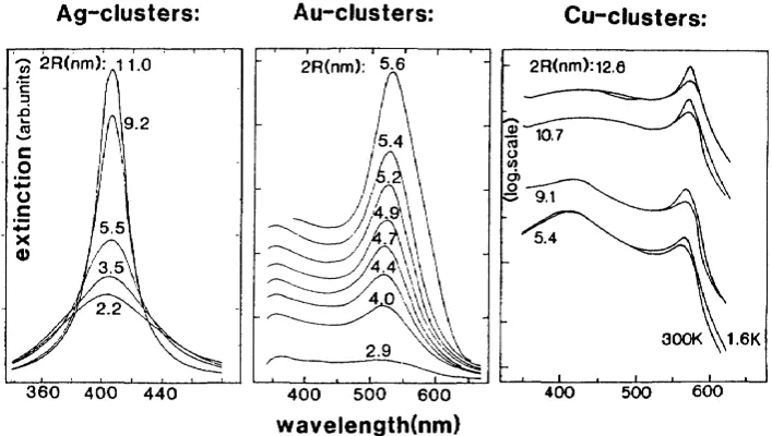
range (Ag [45, 46], Au [47] and Cu [48]), other metals like Pb and Al exhibit
resonances in the IR and deep UV [49, 50] respectively. These subwavelength
structures are attracting attention because of their potential as optical sensors,
in waveguiding [51], biosensors [52], and even solar cells [53, 54].
1.2.1
Overview of the literature
The area of plasmonics is being intensively researched at present, and a number
of recent reviews have been published [55–57]. The field has progressed through
the advances of NP preparation by colloidal synthesis. The process involves the
reduction of an acidic solution: as more atoms are formed the solution becomes
1.2 Plasmonic nanostructures
“common” metals they are usually observed in the visible range (Ag [141, 142], Au [65]
or Cu [143, 144]) and deep UV (Al [145, 146]).
Excitation field Electron cloud
Metal sphere
e- e
-e -- -+ + + -+ +
pind ER
Figure 1.9: Sketch of homogeneous metallic spheres placed in a oscillating EM field. The
conduction electrons are displaced as a whole, polarizing the sphere (
p
ind), while the
surface of the particles exerts a restoring force
E
R, so that resonance conditions can be
established, leading to EM field amplification inside and in proximity of the particle.
In general, the optical response of metal nanoparticles can be quite complex, as the
particles have more than a single resonant mode. These modes differ in their charge and
field distribution, and are strongly dependent on the particle’s size (with respect to the EM
wavelength), shape and environment. The analytical treatment of LSPs for particles with
arbitrary shape is therefore almost always not feasible, and computational methods are
required. Indeed, only few simple configurations allow the exact solution of the optical
response, which include spherical particles [147, 148], spheroids [149] and infinite long
cylinders [150].
The
Mie
theory [147] is an exact solution of the Maxwell equations for the
scatter-ing and absorption problem of spherical particles, and it is usually employed to derive
approximate solutions for similar geometries. According to this theory, the EM fields
are expanded in spherical harmonics, and all the possible LSP modes correspond to the
dipolar and multipolar EM eigenmodes of the particle. A full treatment of the EM
inter-action within the Mie theory is however a very challenging task, because the analytical
description of the highest polar modes is very complex. Therefore, the Mie theory is
often approximated to include only the most significant contributions. The excitation
strength of each mode is determined by the corresponding expansion of the EM field; in
particular, when the particles are much smaller than the involved wavelengths (typically
up to tens of nanometers for EM fields in the visible range) the resonances are mainly
dipolar in character, so only the first order terms can be retained. In such cases the Mie
solution reduces to the
Rayleigh
approximation for the elastic scattering of light [148],
and the quasi-static approximation can be invoked to apply the equations of electrostatics
in electromagnetism.
1.3.1
Quasi-static approximation
Figure 1.3: The response of a homogeneous metallic sphere placed in an oscillat-ing EM field. The conduction electrons are displaced, polarisoscillat-ing the sphere (pind)
.
follows. these act as nucleation centres for the growth of the NPs [58]. Although
successful, this cannot produce the ordered arrays of NPs on surfaces required
for some of the applications. Nanoscale templates produced by non–lithographic
processes can provide a stable surface upon which to grow NPs of various sizes,
by self–assembly. This appears to be a promising approach, as the fabrication of
templates by electron beam lithography, followed by deposition of the metal, is a
specialised and time–consuming process.
The positions of the localised surface plasmon resonances (LSPR) are of
crit-ical importance for many applications. This has been shown to depend on the
dielectric function of the nanoparticle (NP), its size and shape, the inter–particle
separation and the dielectric function of the surrounding medium [44].
Analytic theories of the LSPR lineshapes for NPs within a surrounding medium,
either immersed in a liquid or embedded in a solid matix have been developed
[44] successfully. However, for NPs of arbitrary shape in a complex dielectric
1.2 Plasmonic nanostructures
binding of the target streptavidin molecules. The streptavi-din binstreptavi-ding induces a plasmon band shift, which is
dependent on the streptavidin concentration (Fig. 5c–e)
[33]. This biosensing scheme has been recently extended to
the optical detection of glucose, probing of
antibody-antigen interactions and even diagnosing Alzheimer’s
disease [27]. It must, however, be noted that besides
nanoparticle optical parameters, efficient biosensing also relies on high surface binding efficiency and larger mass
density of the biomolecules [80].
Whereas a detection limit down to 1 pM has been achieved for the streptavidin-biotin sensing using the nanoprism
monolayer [33], the detection limit can be further reduced
by reducing the number of nanoparticles being probed, ideally to the single-nanoparticle level, offering more
spectra of single nanoparticles can be collected with very low background signal. Nanoparticles with a high scattering quantum yield can be easily chosen for such applications based on the well-characterized trends in their optical
properties [19]. On account of the size and shape tunability
of the nanoparticle SPR, it is also possible to use nanoparticles possessing well-separated optical resonances (or colors) and with different surface functionalities for
multiplexed colorimetric sensing and imaging [81] using a
single white light source.
Interparticle plasmon coupling for bio-diagnostics and biology
An additional property of the surface plasmon resonance is
its dependence on interparticle interactions [22–26, 82].
The plasmon oscillation generates an enhanced electric field localized on the nanoparticle surface, decaying over a distance on the order of the size of the nanoparticle itself.
The“near-field”on one nanoparticle can interact with that
on a neighboring particle present in close proximity. This near-field interaction between the nanoparticles modulates the frequency of the surface plasmon oscillation of the coupled-nanoparticle system. This phenomenon is known
as plasmon coupling [24,83]. Experimental and simulation
(Fig.6) studies have shown that the assembly or
aggrega-tion of spherical Au nanoparticles into a close-packed structure results in a red shift of the SPR wavelength from
that of the isolated nanosphere SPR wavelength at∼520 nm
[26,32, 34, 82]. The extent of the coupling-induced red
shift increases with decreasing interparticle distance and
increasing assembly size [26, 82]. The coupling-induced
plasmonic shift is also polarization-dependent as shown by experiments on lithographically fabricated pairs of 150-nm
Au nanodiscs [22]. For the light polarization direction
parallel to the interparticle axis, the plasmon resonance of the nanodisc pair is red-shifted with respect to the single particle case. On the other hand, when the light is polarized orthogonal to the interparticle axis, the observed plasmon spectrum is slightly blue-shifted with respect to the single particle case. Further, the effect of nanoparticle shape anisotropy and assembly orientation on the plasmon coupling has also been studied in assemblies of Au
nanorods [24, 84]. Whereas the end-to-end assembly of
Au nanorods results in a red shift of the longitudinal SPR
band [85], side-by-side assembly, in strong contrast, shows
a blue shift of the longitudinal plasmon band [24]. The
Fig. 5 A nanoscale biosensor based on surface plasmon resonance
sensitivity to local medium dielectric changes [33]. (a) Atomic Force
Microscopy image of a monolayer of Ag nanotriangles fabricated on a glass substrate by the Nanosphere Lithography technique. (b) Scheme showing the formation of thiol monolayer on the nanotriangles followed by their conjugation to biotin molecules via free carboxylic acid groups. (c) Scheme showing the binding of streptavidin molecules to the biotinylated nanotriangles on the substrate. (d) SPR extinction spectrum of the Ag nanobiosensor (1) before and (2) after exposure to 100 nM streptavidin. (e) The normalized fractional SPR
shift ΔR/ΔRmax of the Ag nanobiosensor versus streptavidin
concentration. Figure reprinted with permission from [33]. © 2002
American Chemical Society
114 Plasmonics (2007) 2:107–118
(a) A nanoscale biosensor based on LSPR sensitivity to local medium dielectric changes. The diagram shows the binding of strepvidin molecules to the biotinylated nanotriangles on the sub-strate, after [52]
210 NATURE MATERIALS | VOL 9 | MARCH 2010 | www.nature.com/naturematerials
REVIEW ARTICLE
NATURE MATERIALS
DOI: 10.1038/NMAT2629limited by surface recombination. Second, in a thin-film geometry,
carrier recombination is reduced as carriers need to travel only a
small distance before being collected at the junction. This leads to
a higher photocurrent. Greatly reducing the semi conductor layer
thickness allows the use of semiconductor materials with low
minority carrier diffusion lengths, such as polycrystalline
semi-conductors, quantum-dot layers or organic semiconductors. Also,
this could render useful abundant and potentially inexpensive
semi conductors with significant impurity and defect densities,
such as Cu
2O, Zn
3P
2or SiC, for which the state of electronic
materi-als development is not as advanced as it is for Si.
Other new plasmonic solar-cell designs
The previous section has focused on the use of plasmonic scattering
and coupling concepts to improve the efficiency of single-junction
planar thin-film solar cells, but many other cell designs can benefit
from the increased light confinement and scattering from metal
nanostructures. First of all, plasmonic ‘tandem’ geometries may
be made, in which semiconductors with different bandgaps are
stacked on top of each other, separated by a metal contact layer with
a plasmonic nanostructure that couples different spectral bands in
the solar spectrum into the corresponding semiconductor layer
(see Fig. 6a)
79. Coupling sunlight into SPPs could also solve the
problem of light absorption in quantum-dot solar cells (see Fig. 6b).
Although such cells offer potentially large benefits because of the
flexibility in engineering the semiconductor bandgap by particle
size, effective light absorption requires thick quantum-dot layers,
through which carrier transport is problematic. As we have recently
demonstrated
80, a 20-nm-thick layer of CdSe semi conductor
quantum dots deposited on a Ag film can absorb light confined
into SPPs within a decay length of 1.2 μm at an incident photon
energy above the CdSe quantum-dot bandgap at 2.3 eV. The reverse
geometry, in which quantum dots are electrically excited to generate
plasmons, has also recently been demonstrated
81. We note that the
plasmon light-trapping concepts described in the previous section
rely on scattering using localized modes, and are thus relatively
insensitive to angle of incidence
66,82. This is an advantage for
solar-cell designs made for areas where incident sunlight is mostly diffuse
rather than direct.
In a recent example of nanoscale plasmonic solar-cell engineering,
an organic photovoltaic light absorber was integrated in the gap
between the arms of plasmonic antennas arranged in arrays (see
Fig. 6c)
83. Other examples of nanoscale antennas are coaxial
holes fabricated in a metal film, which show localized plasmonic
modes owing to Fabry–Perot resonances (see Fig. 6d)
84–86. Such
nano structures, with field enhancements up to a factor of about
50, could be used in entirely new solar-cell designs, in which an
inexpensive semi conductor with low minority carrier lifetime is
embedded inside the plasmonic cavity. Similarly, quantum-dot
solar cells based on multiple-exciton generation
87, or cells with solar
upconverters or downconverters based on multiphoton absorption
effects, could benefit from such plasmonic field concentration. In
general, field concentration in plasmonic nanostructures is likely
to be useful in any type of solar cell where light concentration is
a c d b SPP Incident lightSPP guiding layer Quantum-dotactive layer
Top contact 3.0 eV 2.0 eV 1.0 eV Semiconductor Metal P3HT Metal p n p n p n
Figure 6 | New plasmonic solar-cell designs. a, Plasmonic tandem solar-cell geometry. Semiconductors with different bandgaps are stacked on top of each other, separated by a metal contact layer with a plasmonic nanostructure that couples different spectral bands of the solar spectrum into the corresponding semiconductor layer. b, Plasmonic quantum-dot solar cell designed for enhanced photoabsorption in ultrathin quantum-dot layers mediated by coupling to SPP modes propagating in the plane of the interface between Ag and the quantum-dot layer. Semiconductor quantum dots are embedded in a metal/insulator/metal SPP waveguide. c, Optical antenna array made from an axial heterostructure of metal and poly(3-hexylthiophene) (P3HT). Light is concentrated in the nanoscale gap between the two antenna arms, and photocurrent is generated in the P3HT semiconductor83. d, Array of coaxial holes
in a metal film that support localized Fabry–Perot plasmon modes. The coaxial holes are filled with an inexpensive semiconductor with low minority carrier lifetime, and carriers are collected by the metal on the inner and outer sides of the coaxial structure. Field enhancements up to a factor of about 50 are possible and may serve to enhance nonlinear photovoltaic conversion effects85.
(b) NPs can be incorporated in solar cells, acting as scatterers, they increase the optical path of light inside the absorbing ma-terial, thus increasing the overall efficiency of the solar cell. The image is a plasmonic quantum–dot solar cell designed for en-hanced photoabsorption, after [53].
Figure 1.4: The various applications of plasmonic structures are being heavily researched. Biosensors and solar cells some of the many applications.
environment, analytic solutions are not available and Maxwell’s equations are
solved directly using techniques such as the discrete dople approximation and
fi-nite difference time domain methods [60]. Analytic theories of NPs supported on
planar surfaces have been developed, but only for spheroids and ellipsoids where
the NPs are axially symmetric with respect to the surface normal [61].
Numeri-cal approaches have been used for isolated NPs and NP arrays with dimensions
accesible by conventional lithographic techniques [62], but smaller less ordered
and colloidal synthesis. EBL is a powerful technique that can create nanoparticles of arbitrary size, shape, and spacing on a substrate. Its main disadvantages are cost
and the time-consuming operation [23–25]. NSL is a
technique used to generate patterned arrays of metal
nanoparticles on the substrate [26–28]. Colloidal synthesis
is a general methodology for producing nanoparticles with the desired optical properties in a solution, which may then
be recovered later [29–35]. Without requiring expensive
equipment, the preparation of nanoparticles by colloid synthesis can be conducted in any chemistry lab. In addition, this method can be easily scaled up for quantity production relatively inexpensively. Due to the flexibility in selecting different reducing agents, capping agents, solvent systems as well as synthesis conditions, colloidal synthesis can produce nanoparticles in a variety of compositions, shapes and sizes, and surface chemistry [29]. This method can also be used to prepare multi-metallic nanoparticles and particles with complex
architec-tures [30,33]. Besides common chemicals, microorganisms
and biomolecules may also be used to offer a “green
chemistry” approach to the synthesis of nanoparticles in
aqueous solutions.
In this article, we summarize our recent efforts in developing new chemical and biological procedures in colloidal synthesis to prepare nanoparticles with tunable optical properties. The SP absorption bands and the enhancement factors of the nanoparticles were tailored by combining two metals within a single particle or by changing the aspect ratios of anisotropic nanoparticles. We begin the discussion with the synthesis of
zero-dimensional (0-D) bimetallic Ag–Au nanoparticles as
homogeneous alloys, core–shell nanoparticles, and hollow
nanoparticles with an alloy shell. This is followed by the description of the preparation of anisotropic monometallic Ag and Au nanostructures in one dimension (1-D), two dimensions (2-D), and three dimensions (3-D) using
0-D nanoparticles
Zero-dimensional nanoparticles are the most common nanoparticles. They are thermodynamically stable, easily assembled into ordered structures, and their SP absorption for a given particle size can be continuously tuned by varying the composition and composition distribution within the particles. Therefore, while the SP bands of 0-D monometallic Ag and Au nanoparticles only shift slightly with their size, their optical properties can be altered more substantially by combining them within the same particle or by tailoring the internal structure of the particles. We have
synthesized bimetallic Ag–Au nanoparticles as
homoge-neous alloy nanoparticles [36], heterogehomoge-neous core–shell
nanoparticles [37], and hollow nanoparticles with an alloy shell. All of these bimetallic nanoparticles were prepared by the replacement reaction between Ag nanoparticles and
HAuCl4. The structure of the product bimetallic
nano-particles was controlled by the synthesis conditions as well as the size and crystallinity of the starting Ag nanoparticles.
Figure 2a and b shows the transmission electron
microscopy (TEM) and high-resolution TEM (HRTEM) images of the alloy nanoparticles prepared by the replace-ment reaction. Both Ag and Au were detected in each of the particles, indicating that they were bimetallic nanoparticles. The uniform contrast in the TEM and HRTEM images indicates that the bimetallic nanoparticles were homoge-neous in composition throughout. The SP absorption of the alloy nanoparticles could be tuned continuously from ~400 nm to ~520 nm by changing the composition of the
alloy nanoparticles (Fig.2c). The alloy nanoparticles could
be produced in water or in organic solvent by using either single-crystalline or polycrystalline Ag nanoparticles. The most important conditions for the successful preparation of
homogeneous Ag–Au alloy nanoparticles were a small
starting Ag nanoparticle size (less than 12 nm) and reaction at elevated temperatures. This is because the rapid inter-Fig. 1 Colloidal solutions of
Ag, Au, and Ag–Au bimetallic nanoparticles
Figure 1.5: Colloidal solutions of Ag, Au and Ag-Au bimetallic nanoparticles (after [58]). The colloidal solutions are strongly coloured because of the LSPR in the UV/visible spectral region.
Figure 1.6: Measured extinction spectra of Ag, Cu and Au clusters of various sizes in a glass matrix, after [59]
structures are currently too computationally intensive for this approach to be
[image:27.595.147.501.384.584.2]1.2 Plasmonic nanostructures
(a) AFM image of faceted Al2O3
substrate. Inset: SEM image of Ag NPs grown at glancing angle of 6◦ on the faceted template.
(b) AFM of a native–oxide–covered rippled Si(001) surface with
∼30 nm periodicity. Inset: SEM of Ag NPs deposited on the rippled surface.
(c) 3µm×3µm STM topographic image of the Si(335) substrate with Pb nanowires, after [63].
Figure 1.7: Examples of nanoscale templates: faceted Al2O3, Si(001) and Si(335)
for the production of aligned nanoscale arrays.
a controllable and reproducible fashion. For example, the annealing procedure
for vicinal single crystal Al2O3 substrates can be adjusted to control nanoscale
terrace width and periodicity associated with facetting (Figure 1.7a) [22, 64,
65]. Similarly, Pb deposited on vicinal Si(111) forms aligned, elongated islands
with length to width ratios greater than 100 (Figure 1.7c) [63]. Low energy ion
beam irradiation is another established method for forming nanoscale periodic
patterns on flat substrates [66, 67]. Using these rippled templates NP arrays with
short range order and adjustable periodicity can be made on various substrates,
including native-oxide-covered Si(001) (Figure 1.7b) [68, 69]. Local damage and
disorder is caused by irradiation of the surface, but it has been shown recently that
the quality of these rippled structures can be improved significantly by sequential
sputtering at lower fluences, with the sample rotated 90◦ so that the ion beam is
aligned along the ripples at grazing incidence [70].
1.2.1.1 Optical techniques
Although absorption spectroscopy is routinely used to characterise the plasmonic,
epioptic techniques remain largely unexplored for growth monitoring and
char-acterisation of plasmonic nanostructures. The in–plane LSPRs of anisotropic
Nps are accessible to RAS, while the out–of–plane LSPR requires SE.
Histori-cally, the RAS response of plasmonic nanostructures was seldom reported, due
to limitations in colloidal preparation techniques in the past. It was Witkowski
et al who first used RAS to study self-organised, anisotropic cobalt nanodots on
vicinal Au(111) [71], demonstrating that with improved methods of sample
fab-rication, the plasmonic response can be monitored directly. Recent studies have
1.2 Plasmonic nanostructures
measurable RAS response [72]. Chapter 5 describes the use of RAS and SE to
characterise LSP systems.
Real–time monitoring of the growth of these anisotropic rippled templates,
during Ar+ ion irradiation, which is used at pressures typically in the range of
10−4 mbar, is challenging. Epioptic techniques offer significant advantages over
conventional surface techniques in characterising the formation of these surface
structures, as they are insensitive to charged particles and surface potentials. Our
group, in collaboration with colleagues, have shown recently that RAS is a useful
in situ probe of Ag NP growth on facetted Al2O3 [22], raising the possibility that
such optical techniques may be able to monitor the growth of both the template
and the NP array, in real time.
Upon excitation LSP excitation produces a very strong amplification of the
electric field, which is dependent on size, shape and environment of the NP. This
has led to the development of LSP–enhanced spectroscopy , for example Surface
Enhanced Raman Scattering (SERS) [73]. This technique developed originally
using rough Ag surfaces, but the use of LSPRs, particularly localised at the tip of
a scanning probe system, has led to Raman spectra from single molecules being
detected at surfaces [3]. Similarly, this field enhancement can also be used to
amplify the weak signals from nonlinear optical techniques like SHG. SHG from
metal surfaces has been widely studied both theoretically and experimentally [74–
76], since their response is much stronger due to loosely bound electrons which
are more polarisable. However, SHG from self–organised metallic NPs is seldom
reported. SHG is a potential optical technique for monitoring the growth of
conducted spectroscopic SHG on Au nano–wire arrays on ion beam irradiated
glass at normal incidence, in order to tune the metal plasmon resonance close to
the pump frequency, and also investigated the effect of local tilt of the nanowires.
The conversion efficiency was found to increase as the plasmon resonance was
shifted closer to the pump wavelength, and highly dependent on the tilt and
hence shape of the nanowire in cross-section, indicating the sensitivity of this
technique. Furthermore Kimet al have studied third harmonic generation (THG)
in silver island films [78]. SHG is useful even when spectroscopic studies may not
be possible. Polarisation dependent studies of these structures can provide in–
and out–of plane information on symmetry of the NP, as dicussed in detail in
Chapter 5.
1.3
Thin film chiral systems
A chiral molecule is defined as one which has a non-superimposable mirror image.
The term chirality comes from the Greek word kheir, meaning handedness, and
was coined by the Irish physicist William Thomson (Lord Kelvin) in his 1884
Baltimore lectures. Perhaps the most universally recognised image of chirality is
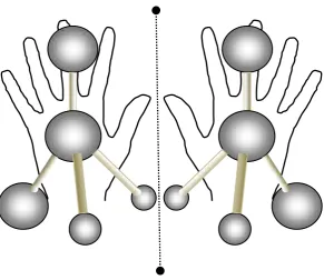
a pair of hands: the left hand cannot be superimposed on the right one (Figure
1.8). Simple chiral molecules exist in two enantiomeric forms, which differ in
their interaction with other chiral systems, but otherwise have the same physical
and chemical behaviour. Most of the molecules which are important to living
systems are chiral, e.g. amino acids, proteins, sugars and nucleic acids. Chiral
drugs have become a dominant feature in today’s pharmaceutical industry, with
1.3 Thin film chiral systems
80% of todays developmental drugs are now chirally pure [79], and improvements
in chiral synthesis, purification and characterisation are being sought.
1.3.1
Overview of the literature
The invention of scanning tunneling microscopy (STM) has opened up ways to
study interactions on a molecular level at well–characterised surfaces. Further
advancements in the field have led to probing chiral phenomena, e.g.
adsorp-tion and reacadsorp-tion on crystalline surfaces, where absolute chiral recogniadsorp-tion can
be attained [80]. For example, chirality and conformation of terephthalic acid
monolayers on graphite [81] has been studied, while Fanget al [82] have used Br
atoms as an STM marker on the stereogenic centre to determine the chirality of
2-bromohexadecanoic acid adsorbed on a graphite surface. Chiral discrimination
by chemical force microscopy has also been successful [83]: by attaching chiral
molecules to the probe tip, the two enantiomers of mandelic acid
(2-hydroxy-2-phenylacetic acid) were differenciated through differences in adhesion and
fric-tional forces measured by the probe. The most relavent example, however, for
this thesis, is the adsorption of cysteine on Au(110) surfaces in UHV [84, 85].
Fig-ure shows chiral recognition in the dimerisation of adsorbed cysteine observed by
STM (Figure 1.9) [84]. Such STM studies have provided important new
informa-tion but, in general, alternative methods of detecinforma-tion of chirality at surfaces are
needed in order to perform these experiments under realistic synthesis conditions,
Figure 1.8: Schematic showing the effect of chirality with an enantiomer pair. The enantiomers, like a pair of hands, are identical but non-superimposable mirror images of each other.
1.3.1.1 Optical techniques
The most popular method of distinguishing between enantiomers is using optical
circular dichroism (CD) around the visible of the spectrum. A chiral molecules
will absorb left– and right–circularly polarised light in different amounts, and
CD involves measuring this difference as a function of wavelength. When
circu-larly polarised light interacts with a chiral molecule in solution, the CD can be
expressed as,
Al−Ar
AT ot
1.3 Thin film chiral systems
Figure 1.9: (S)–(−)–cysteine pairs fromed on the Au(110) observed by STM, after [84].
whereAl andAr are absorbances for left– and right–circularly polarised light, re-spectively, andAT otis the total absorbance. The responses from CD are extremely weak, typically of the order of 10−3 of the total absorbance. Other limitations of
this technique include the inability to measure samples in reflection, as the effect
is annulled. CD cannot be used to characterise thin films of chiral molecules on
planar surfaces.
Chiral detection at the very early stages of a reaction would be a
break-through, as chiral organic synthesis is complicated and expensive. The key would
be to achieve chiral discrimination at the monolayer level, which is difficult on
surfaces. Nonlinear optics has the sensitivity to do this. The fact that chiral
molecules are, by definition acentric, means SHG is capable, in principle, of
de-tecting enantiomeric excess at surfaces, if it has sufficient sensitivity.
films of 1,1’–binaphthalene–2,2’–diol (binol) at fused silica and liquid interfaces,
that initiated the use of nonlinear optics, specifically SHG, to reveal chirality from
monolayers [41, 42]. They used SHG–CD, which is the nonlinear optical technique
analogous to CD which measures the difference in SH efficiency of the sample for
left– and right–circularly polarised light as a function of wavelength. Chiral–SHG
was observed on thin films of binol on quartz. Using a quarter wave plate the
SH efficiency was measured as a function of frequency of the laser, as was tuned
towards the resonance energy of binol. A racemic surface, (i.e, a 50:50 mixture of
the two enantiomers), yielded no difference in SHG efficiency for the left– or right–
circularly polarised light. In bulk binol solutions measured using CD, the effect
was found to be small, with absorption coefficients for left– versus right–circularly
polarised light varying by a factor of ∆/ ≈ 0.1% , whereas the asymmetry in SHG can reach values up to 100% on resonance. This work was extended to
larger molecules, such as cytochrome c, and combined with surface enhanced
Raman spectroscopy [86]. More recently, the work by Schanne–Klein et al on
an acridine substituted Tr¨oger base was shown to have an excitonically enhanced
chiral response, that produced a rotation of 66◦ in the SH polarisation, which was
estimated as being six orders of magnitude larger than the linear response (Figure
1.10) [87]. No work has been published on small chiral molecules adsorbed on
well–characterised single crystal surfaces, which is an essential first step in probing
chiral catalysis at solid surfaces. Small molecules are less polarisable than large
ones and it is not clear whether SHG will have sufficient sensitivity to detect the
chiral response of a ML of small molecule adsorbed on a single crystal surface.
Two chiral molecules have been studied during the course of this work:
in-1.3 Thin film chiral systems
Figure 1.10: α–p response of the acridine substituted Tr¨oger base, as a function of quarter–wave plate angle, showing a 66◦ rotation between enan-tiomers. Top: (+) enantiomer, bottom: (−) enantiomer. Arrows at +45◦ and −135◦ indicate that the polarisation of the fundamental laser beam is right–circular. The lines indicate the fitted data. Di-agram on the right hand side shows the (+)–7S,17S enantiomer of the acridine substituted Tr¨oger base.
terest. Of the 20 natually occurring amino acids, only cysteine contains a thiol
group which allows a disulfide bond to be formed with other cysteines, which is
important in the formation of active structural domains. In addition, the thiol
group, –SH, enables excellent binding to gold surfaces. As mentioned above, it
has been shown recently by STM that a racemic mixture of cysteine adsorbed on
the Au(110) surface, under UHV conditions, forms homochiral molecular pairs
[84], giving compelling evidence for chiral discrimination in molecular
of (R)–(+)–cysteine on Au(110) in both UHV and electrochemical environments
[88] and, due to the self–limiting growth of the molecule, a fingerprint spectrum
for a cysteine ML adsorbed on Au(110) was obtained. No chiral studies were
undertaken and, as RAS is based on reflection, no direct chiral optical response is
expected. Indirect effects associated with different adsorption sites at the surface
at the surface cannot be ruled out, however.
In conclusion, the potential for RAS and SHG to compliment well
estab-lished techniques, for the investigation of surfaces, interfaces, ultrathin films and
nanostructures is gathering momentum, which makes epioptics an exciting field
to study. The research described in this thesis demonstrates how surface sensitive
optical techniques of this kind can be used to characterise plasmonic
nanostruc-tures and ultrathin chiral films of small molecules. It is important that these
techniques continue to be developed and applied in order to enhance our
Chapter 2
Theory and phenomenology of
experimental techniques
“A painter should begin every
canvas with a wash of black,
because all things in nature are
dark except where exposed by
the light.”
–Leonardo da Vinci
The propagation of electromagnetic waves through a material gives rise to a
number of optical processes, including reflection, refraction, absorption and
trans-mission. By measuring the variation of these processes it is possible to define the
optical properties of the material. When the intensity of the incoming radiation
is low, the resulting optical processes are linear in nature and are described using
observed; these effects are described by nonlinear optics (Section 2.2).
2.1
Linear optical response of materials
Under low incident light intensities, the forces exerted on electrons are small
compared to their binding energy. As a result, the electric polarisation induced
in the material P depends linearly on the electric field of the light wave,
P =0χ(1)E (2.1)
where0 and χ(1) are the dielectric permittivity and the first order susceptibility
respectively. χ(1) is a measure of the extent to which the incoming electric field causes polarisation and can be seen in the form,
= 1 +χ(1) (2.2)
where is the complex dielectric function, and is described as,
=1 +i2 (2.3)
This can be related to the complex refractive indexN by taking the square root of the dielectric function,
2.1 Linear optical response of materials
where n is the real part of the complex refractive index and k is the extinction coeffient. The complex refractive index is a frequency dependent quantity
ac-counting for the absorption of light with increasing distance into the material.
Equation 2.4 can then be solved to obtain,
1 =n2−k2 (2.5)
2 = 2nk (2.6)
leading to,
n= √1
2(1+ (
2 1+ 2 2) 1 2) 1 2 (2.7)
k= √1
2(−1+ (
2 1+ 2 2) 1 2) 1 2 (2.8)
If the medium is only weakly absorbing from Equation 2.6, 2 is very small and n ≈ √1 is thus determined by the real part of the dielectric constant. The
reflectivity,R, also depends on both n and k, and at normal incidence we have:
R =
N −1
N + 1
2
= (n−1)
2+k2
(n+ 1)2+k2 (2.9)
2.1.1
Reflection anisotropy spectroscopy
RAS is a linear optical technique which measures the difference in reflectance ∆r, normalised to its total reflectance r, between orthogonal symmetry directions in the surface plane at near normal incidence. Reconstructions of the surface layer
the reflectance anisotropy and is defined as,
∆r r =
2(rx−ry)
rx+ry
(2.10)
whereris the mean reflectance, and rx andry denote reflection coefficients along the orthogonal polarisation axes in the x and y direction respectively. RAS is very useful for monitoringin situgrowth and layer completion because anisotropic
surface reconstructions can vary from layer to layer. A comprehensive review of
RAS has been published by Weightman et al [10].
Figure 2.1 illustrates the measured polarisation state and the sample
ori-entation of a Au(110) surface. The two main symmetry directions of Au(110)
are [1¯10] and [001]. An anisotropy of the surface will result in a slightly
dif-ferent amplitude and phase component being reflected, converting the incident
plane–polarised light into elliptically polarised light. For Au(110) the resulting
reflectance anisotropy becomes,
∆r r =
2(r1¯10−r001) r1¯10+r001
(2.11)
The amplitude of the ellipse is related to the real part of the RAS signal, while
the phase of the ellipse represents the imaginary part of the signal. The RAS
signal is generally measured using a photoelastic modulator (PEM) (see Section
3.3). An alternative approach is to use a rotating sample setup. However, this can
be difficult to implement for in situ studies and is less sensitive [89]. The PEM
and analyser polariser combination converts a polarisation modulated signal into
2.1 Linear optical response of materials
Change in amplitude and phase upon reflection
Linear polarisation incident on surface
plane
[001]
[110]
Figure 2.1: Principle of RAS demonstrated on Au(110). Normally–incident light is linearly polarised and upon reflection becomes elliptically polarised due to a phase and amplitude change which is related to the in–plane anisotropy. Note that the angle of incidence has been exaggerated for clarity.
2.1.1.1 Origin of a RAS signal
RAS is sensitive to surface structure by symmetry considerations. The bulk
structure of cubic materials will yield no RAS response i.e. xx = yy, while the surface will often reconstruct to break cubic symmetry, so any sizeable RAS
response from cubic materials will be due to the surface or interface region. Non–
vicinal anisotropically reconstructed (100) or (111) surfaces of cubic materials
should give a response, but two or three equivalent domains, respectively, often
form at the surface which prevents a RAS signal from being observed, as the beam
1 . 0 1 . 5 2 . 0 2 . 5 3 . 0 3 . 5 4 . 0 4 . 5 - 1 0
- 8 - 6 - 4 - 2
0
2
4
R
e(
∆
r/r
) (
10
-3 )
p h o t o n e n e r g y ( e V )
d o u b l e - d o m a i n S i ( 0 0 1 ) - 2 x 1 A u ( 1 1 0 ) - 2 x 1
Figure 2.2: Comparison of the RAS response of Au(110)–2×1 and double–domain Si(100)–2×1.
and tend to form single domain surfaces. The RAS response from reconstructed
Au(110)–2×1 and double domain Si(100)–2×1 are compared in Figure 2.2. The
clean Au(110) surface reconstructs at room temperature to produce a 2×1
‘miss-ing row’ reconstruction [90], which was confirmed with LEED (see Figure 3.12).
The RAS features above 3 eV are thought to arise from surface modified bulk
transitions, while the RAS response in the region 1.5–2.5 eV is sensitive to
sur-face reconstruction [91, 92]. Studies of various semiconductors have found that
the electronic bands of the bulk crystal are modified by the presence of a surface
layer, which in turn contributes to the RAS profile [93], and it is thought that
similar contributions occur in metals.
Several phenomenological models have been developed in order to relate the
2.1 Linear optical response of materials
is the three phase model of McIntyre and Aspnes [94]. In this approach, a thin
anisotropic layer of thicknessd, is located between a semi–infinite isotropic bulk, of dielectric function b, and a semi-infinite ambient layer of dielectric function
m. The surface anisotropy s is then expressed by the two different diagonal tensor components in thexand ydirection, ii. The RAS signal for a detector in the ambient region is given by,
∆r r =
4πd√m
λ
i(s
xx−syy)
b−m
(2.12)
where λ is the wavelength of the light (dλ). Equation 2.12 can be used to calculate the RAS response when ∆s is determined using ab initio electronic structure theories [10].
2.1.2
Spectroscopic ellipsometry
Spectroscopic ellipsometry (SE) is a linear optical technique widely used for the
characterisation of thin films [95]. This well established method that, in its
gen-eral form, is useful for analysing a number of parameters including layer thickness,
dielectric function and surface and interfacial roughness (and thus constituent
and void fractions). However, in order to extract this information, modelling is
required to allow full optical characterisation of thin films [96].
Ellipsometry works on the principle that linearly polarised light reflected from
the surface of the thin film becomes elliptically polarised as shown in Figure 2.3.
The change in polarisation is measured by analysing the light upon reflection
E E
p-plane p-plane
θ linearly polarised
light
elliptically polarised
light
∆
s-plane
ψ
Figure 2.3: The principle of ellipsometry. When linearly polarised light is inci-dent on the sample, the reflected light is elliptically polarised. The ellipticity of the reflected light depends on the optical constants of the sample.
major axis of the ellipse and the positive direction of the x axis [97], while ∆ is the phase difference between thesandpcomponents (Figure 2.4). Attenuation of thes andpcomponents of light determines the tilt of the ellipse, while the phase shift of the s and ppolarised light is related to the ellipticity of the ellipse. The amount of induced ellipticity depends on the optical constants of the material.
Ψ and ∆ are related to the Fresnel reflection coefficients, rs and rp for s and p polarised light respectively, whereris defined as the ratio of reflected to incident electric field amplitude. The complex ratio of the reflection coefficients of light
polarised parallel and perpendicular to the plane of incidence is defined by;
ρ= rp
rs
2.1 Linear optical response of materials
Ers
E
rpψ
Major axis of the ellipse
Figure 2.4: When sand pwaves are reflected, they experience a phase shift and amplitude reduction (not necessarily the same for both waves) de-fined by the ellipsometric parameters Ψ and ∆. These parameters determine the ellipticity.
The value ofρ is complex and frequency dependent and contains both the ampli-tude ratio and phase difference ∆. The quantities in Equation 2.13 are defined
as:
tan(Ψ) =
rp
rs
(2.14)
cos ∆ =δp−δs (2.15)
and are related to the intensity ratio and phase difference δ in the s– and p– polarised reflected beams. The overall response of the volume sampled by the
beam is described by the pseudo dielectric function of the sample, which is given
by
< (ω)>= sin2θ+ sin2θtan2θ(1−ρ(ω)) 2
whereθ is the angle of incidence and ρis given by Equation 2.13. For a general, multi–component system, modelling is required to relate the dielectric function
and thickness of the layers to< (ω)> [97].
2.2
Nonlinear optical response of materials
While the interaction of radiation of low intensity with matter is much more
common, high intensity, coherent radiation of the order of MW/cm2, from a laser,
causes electrons in a solid to behave nonlinearly as a result of the high electric
fields driving them. These nonlinearities contribute to the induced polarisation of
the material and can produce complex effects such as sum frequency generation
(SFG) and second–harmonic generation (SHG), where a response at twice the
exciting frequency can be produced. The electric polarisation P, induced in a material by an electromagnetic field E(ω) is given by:
P(k, ω) =0[χ(1)E(k, ω) +χ(2)E2(k, ω) +χ(3)E3(k, ω) +....] (2.17)
whereχ(i)is theith order susceptibility tensor of ranki+1 describing the material response.
2.2.1
Second–harmonic generation
The advent of the laser led to the first observation of SHG, in 1961 by Franken
et al [23], and SHG has been intensively studied since, as described in the book
by Shen [98]. The first term on the right hand side of Equation 2.17 describes
![Figure 1.2: The field of epioptics covers a range of different techniques includingRAS, Ramen and SHG, see [2] for details.](https://thumb-us.123doks.com/thumbv2/123dok_us/1374377.671026/19.595.145.498.167.403/figure-eld-epioptics-covers-dierent-techniques-includingras-details.webp)
![Table 2.2: Independent components of tensors χeee, χeem and χmee, for both achi-ral and chiral surfaces [110].](https://thumb-us.123doks.com/thumbv2/123dok_us/1374377.671026/56.595.142.496.179.418/table-independent-components-tensors-xeee-xeem-chiral-surfaces.webp)