Design and Implementation of 2by3 Prescaler
using Different Logic in CMOS 45nm
Technology
Siddharth A. Koshiyar, Narendra J. Patadiya, Prof. Bharat H. Nagpara,
Student, Department of ECE, C. U. Shah College of Engineering and Technology, Wadhwan city, Gujarat, India. Student, Department of ECE, C. U. Shah College of Engineering and Technology, Wadhwan city, Gujarat, India. Professor, Department of ECE, C. U. Shah College of Engineering and Technology, Wadhwan city, Gujarat, India.
ABSTRACT: Frequency division is one of the important applications of flip-flops. A wide-band frequency synthesizer implemented by phase-locked loop (PLL) uses prescaler (also called N/N+1 counter) as fundamental block. In PLL high frequency output of VCO is coupled directly to the prescaler directly. As process technology is reducing, channel length and supply voltage is decreasing rapidly. Therefore prescaler has to work at high frequency as well as low operating voltage. Using pass transistor or CMOS Technology are the incorporation of additional logic gates between the flip-flops to achieve the two different division ratios, the speed of the prescaler is affected by creating another propagation delay and the increases the switching power.
KEYWORD: LT-Spice-IV, VCO (voltage controlled oscillator), DMP (Dual Modulus Prescaler) TG (transmission gate),PTL(pass transistor logic).
I. INTRODUCTION
The CMOS Technology has been the main integrated circuit technology for at least 15 years due to its advantages in terms of integration level, power consumption, High Speed, easiness of Implementation, or Design and low cost& easy and easy stimulation using Software. With the continuous reduction (Or change in term of width & length of transistor) of the transistor dimensions, some of these advantages, such as integration level, have increased and new ones have been added, such as the technology speed, extending the technology uses to areas where only faster and more expensive technologies (Bipolar and GaAs) were applicable. One of these new application areas is RF circuits: circuits for transmission and reception of information through radio frequency waves. This area presents wide spectrum of applications varying from command devices for automatic gates to sophisticate cellular phones.
In the more complex RF systems, or Wireless Zigbee system an important block is the frequency synthesizer. This block is responsible for the generation of signals in specific frequencies that are used for channel modulation and demodulation inside the transmission band[1],[2]. A synthesizer is composed of a voltage controlled oscillator (VCO), counters, phase comparators, and filters or frequency divider. Some architectures of synthesizer use, with the counters, a dual-modulus prescaler N/N+1: a frequency divider that can divide an input clock by N or N+1.
In general the prescaler is a block with critical operation in terms of speed and power consumption since it receives the clock directly from the VCO output, the fastest signal in the synthesizer. In this work, we will present the design and simulation results of a dual-modulus prescaler 2/3. In the prescaler was used the TSPC technique or another different logic style of D-flip-flop like transmission gate, pass transistor logic or also GDI logic.
Vol. 3, Issue 3, March 2015
II. PRESCALER ARCHITECURE
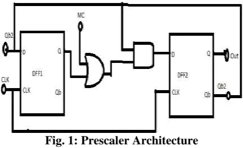
The block diagram of the 2/3 Prescaler architecture is shown in Figure.1 [9]; the dual-modulus prescaler is based on both synchronous and asynchronous divider which scales the input frequency to a lower frequency to ease the complexity of asynchronous resettable modulo-P and modulo-Scounters.
Fig. 1: Prescaler Architecture
From the circuit topology view point, prescaler and presettable counters are often implemented using different logic families or using various type or style of designing or implementation of D-flip flop, owing to their different speed specifications and a level shifter is required after the DMP to compensate different voltage rails. The basic programmable frequency divider architecture is shown above.
III. IMPLIMENTAION OR DESIGN OF D-FLIP FLOP USING VARIOUS LOGIC
In this chapter we discus about the making or design of D-flip-flop using various logic like TSPC (true single phase clock),pass transistor, transmission gate. These all logic style of D-flip-flop affects on circuit output that means change (reduce) power dissipation and make circuit fast (reduce delay) and make circuit more reliable
.
A.D-flip flop Using TSPC (True Single Phase Clock)
Dynamic or clocked logic gates are used to decrease circuit complexity, increase operating speed, and lower power dissipation. Of various dynamic CMOS circuit techniques, a TSPC dynamic CMOS circuit is operated with one clock skew exists except for the clock delay problems, and even higher clock frequency can be achieved. Single-phase- clock strategies like TSPC achieve higher clock frequencies because they can simplify the clock distribution and removed phase overlapping problems or other benefit of TSPC is no need to extra source for give frequency to the circuit, it works only on one single clock, that’s why power dissipation is become less[9].
Fig. 2: D-flip-flop using TSPC Logic
Fig.2[9] shows a conventional dynamic TSPC D-flip-flop. The flip-flop consists of nine transistors, where the clocked switching transistors are placed closer to power/ground for higher speed. The state transition of the flip-flop occurs at rising edge of the clock signal, clk.
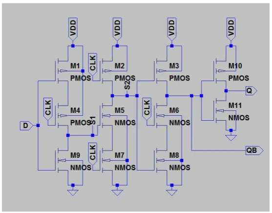
B.D-flip flop using Transmission gate
Transmission gate and inverters are utilized to implement D flip-flop circuit as illustrated in Figure 3 shows. Transmission gate is a most commonly used CMOS structure for implementing integrated circuits that maintains switch function, efficient layout and logic reduction .In figure 2 transmission gates T1 and T4 are turned ON and transmission,
Fig. 3: DFF using Transmission gate Logic(TG)
Vol. 3, Issue 3, March 2015
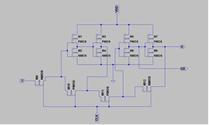
C. D-flip-flop using Pass Transistor Logic (PTL)
It is confirmed that pass transistor based CMOS logic can be frequently utilized where high speed and high packaging density is a major concern.
Fig. 3: DFF using Pass Transistor Logic (PTL)
The logic results in reduction in the number of transistors of the circuit by introducing differential logic and eliminating additional transistors.
In pass transistor logic style we use either NMOS or PMOS transistor to build a design. Logic levels are passed between nodes of circuit as transistors are utilized as switches. The amount of active devices is thus reduced; however as the number of stages increase it becomes difficult to observe a significant difference between high and low logic levels. Master-slave latches have been implemented using inverters and pass transistor logic (PTL) as shown in figure2. The two chained inverters are in memory state when the PMOS loop transistor is on, that is when clock (clk) = 0. Other two chain inverters on the right hand side acts in the opposite way. The flip-flop changes its state during the falling edge of the clock.
IV. SIMULATIONS RESULTS OF THE 2/3 PRESCALER Divided by 2 output:
Divided by 3 output:
Fig. 6: divided by 3 waveform
V. CONCLUSION
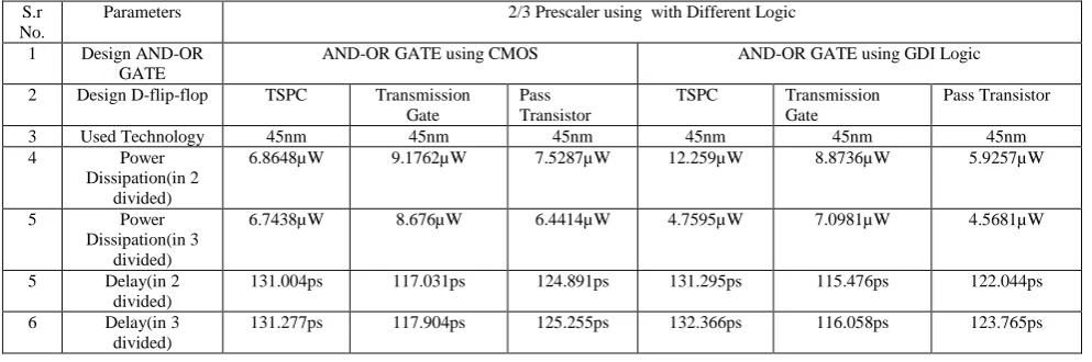
This paper presents a 2/3 Prescaler (Programmable Frequency Divider) designed in 45-nm CMOS process with various logic of D-flip-flop. After analysis these all stimulation results of all 2/3 circuit we conclude that power dissipation of 2/3 Prescaler design using the PTL is very low ,and Speed of 2/3 Prescaler design using the transmission gate is very high that means delay is very less compare to another logic at 1v supply in 45nmTechnology. The DFF in the prescaler is controlled by the mode controlling signal and powered off in the idle state, the DFFs in the program counter and swallow counter are shared, and thus power consumption is reduced. The experimental results show large power reduction is achieved by the proposed divider. We can conclude that the proposed divider is more perfect for low power design
TABLE I
Comparative Analysis of 2/3 Prescaler
S.r No.
Parameters 2/3 Prescaler using with Different Logic
1 Design AND-OR
GATE
AND-OR GATE using CMOS AND-OR GATE using GDI Logic
2 Design D-flip-flop TSPC Transmission
Gate
Pass Transistor
TSPC Transmission
Gate
Pass Transistor
3 Used Technology 45nm 45nm 45nm 45nm 45nm 45nm
4 Power
Dissipation(in 2 divided)
6.8648µW 9.1762µW 7.5287µW 12.259µW 8.8736µW 5.9257µW
5 Power
Dissipation(in 3 divided)
6.7438µW 8.676µW 6.4414µW 4.7595µW 7.0981µW 4.5681µW
5 Delay(in 2
divided)
131.004ps 117.031ps 124.891ps 131.295ps 115.476ps 122.044ps
6 Delay(in 3
divided)
Vol. 3, Issue 3, March 2015
REFERENCES
1. Seok-Ju Yun, Kwi-Dong Kim, and Jong-Kee Kwon “A Low-Spur CMOS PLL Using Differential Compensation Scheme”. ETRI Journal,
Volume 34,Number 4,August 2012.
2. Te-Wen Liao, Jun-Ren Su, and Chung-Chih Hung, “Ring-VCO Based Low Noise and Low Spur Frequency Synthesizer” , IEEE ,pp.1861-
1864,201
3. Haijun Gao, Lingling Sun and Jun Liu. “Pulse swallow frequency divider with idle DFFs automatically powered off”. ELECTRONICS
LETTERS 24th May 2012 Vol. 48 No.11.
4. Don P John, “High Frequency 32/33 Prescalers Using 2/3 Prescaler Technique”. IJER, Jul-Aug 2013, pp.655-661.ISSN: 2248-9622, Vol. 3,
Issue 4.
5. Razavi Behzad, Principles of Data Conversion System Design, IEEE Press, 1995.
6. R. Jacob Baker, CMOS Circuit Design, Layout and Simulation, Third Edition, Wiley Publication, 1964, pp. 1-31, 931-1022.
7. B. Chang, J. Park, and W. Kim, “A 1.2 GHz CMOS dual-modulus prescaler using new dynamic D-type flip-flops,” IEEE J. Solid-State Circuits,
vol. 31, no. 5,pp. 749–752, May 1996.
8. Sung-mo kang,Yusuf leblabici. “CMOS digital integrated circuit analysis and disign”.3rd Edition.
9. Rajesh A. Dabhi,’’ A Low Power 1MHz Fully Programmable Frequency Divider in 45nm CMOS Technology’’IJIRST,Vol. 1, Issue 1, February
2014.
BIOGRAPHY
Mr.Siddharth A. Koshiyar and Mr. Narendra J. Patadiya arepursuing B.E.(final year) Degree in Electronics and Communication Engineering from Gujarat Technological University, Ahmadabad