ISSN(Online): 2319-8753
ISSN (Print): 2347-6710
I
nternational
J
ournal of
I
nnovative
R
esearch in
S
cience,
E
ngineering and
T
echnology
(An ISO 3297: 2007 Certified Organization)
Vol. 6, Special Issue 11, May 2017
An Implementation of Well Organized
Delay-Area Carry Select Adder
Ranjit Chandrakant Gawande, Mr. Vinodkumar P. Patil,
ME-II, Nagaon Education Society's Gangamai College of Engineering, Nagaon, Tal Dist– Dhule, (M.S.), India Assistant Professor, Department Electronics & Telecommunication Engg.,Nagaon Education Society’s Gangamai
College of Engineering, Nagaon, Tal Dist-Dhule (M.S.), India
ABSTRACT: The logic operations used in conventional carry select adder (CSLA) and BEC-based carry select adder (CSLA) i.e., binary to excess-1 converter based carry select adder are estimated in this paper, to study the data dependence and to identifythe unnecessary logic functions. In this paper, all the unnecessary logic functions built-in in the conventional CSLAare removed and we proposed a new logic formation for CSLA. In the proposed method, the carry select (CS) function is considered before the calculation of final-sum which is different from the conventional method. Bit patterns of two considered carry words (cin = 0 and 1) and fixed cin bits are used for logic development of CS and generation units. Acapable CSLA design is obtained using improved logic units. The projected carry select adder (CSLA) design utilizes significantly less area and delay than the recently proposed BEC-based carry select adder. Because of the small carry-output delay, the planned CSLA design is a high-quality nominee for square-root (SQRT) CSLA. A theoretical approximation shows that the proposed SQRT-CSLA occupy almost 35% less area–delay–product (ADP) than the BEC-based SQRT-CSLA, which is most excellent between the existing SQRT-CSLA designs, for the different input bit-widths.
I. INTRODUCTION
Plan of high speed digital adders withwell-organized area and delay is one of the mainparts of study in VLSI system design. Adders are the most important part in microprocessors and digital signal processors systems. The RCA i.e., Ripple Carry Adders have the most compact design among the all type of adders, they are the slowest type of adders. On the other hand,Carry Look-ahead Adders (CLAs) are the fastest adders, but their area requirement is large. Carry Select Adders have the advantages of both RCAs and CLAs, as it has the best area like RCAs and the short delay like CLAs.The speed of addition in digital adders is limited by the time required to circulate a carry through the adder. The addition for every bit points in all addersis created in series, only after the prior bit position has been summed and a carry is propagated into the next position. The CSLA is used in a number of arithmeticsystems to solve the complexity of carry propagation delay by independentlygenerating several carry and then choose a carry to generate the final sum [1] [2].
ISSN(Online): 2319-8753
ISSN (Print): 2347-6710
I
nternational
J
ournal of
I
nnovative
R
esearch in
S
cience,
E
ngineering and
T
echnology
(An ISO 3297: 2007 Certified Organization)
Vol. 6, Special Issue 11, May 2017
optimization largely depends on accessibility of unneeded operations in the formulation, while adder delay mostly depends on data dependence. In the presented designs, logic is optimized without giving any consideration to the data dependence. In this paper, we arranged an analysis on logic operations occupied in conventional and BEC-based CSLAs to study the data dependence and to identify unneeded logic functions.
Based on this study, we have designed a new logic formulation for the CSLA. The mainpart of this paper is logic formulation based on data dependence and optimized carry generator (CG) and carry select unit (CS) design. Based on this proposed logic formulation, we have created a capable logic design for CSLA. Due to improved logicunits, the expected CSLA occupy considerably less ADP than the existing CSLAs. We have shown that theSQRT-CSLA using the proposed CSLA design engage almost 32% fewer ADP than that of the corresponding SQRT-CSLA. Logic formulation of CSLA is presented in SectionII. The proposed CSLA is presented in Section III and the performance estimation method is presented inSection IV and the conclusion is given in Section V.
II. LOGIC FORMATION
The CSLA has two units: 1) the sum and carry generator unit (SCG) and 2) the sum and carry selection unit[12]. The SCG unit usesa large amount of the logic resources of CSLA and considerablyput in to the criticalpath. Different logic designs have been recommended for well-organized implementation of the SCG unit. We have made astudy of the logic designs recommended for the SCG unit of conventional and BEC-based CSLAs of [9] by properlogic expressions. The main purpose of this study is to identify unneeded logic functions and datadependence. Therefore, we remove all unneeded logic function and sequence logic operations based ontheir data dependence.
(a) (b)
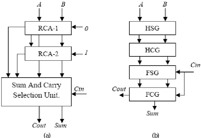
Fig. 1. (a) Conventional CSLA (b) The logic operations of the RCA is shown in split form, where HSG, HCG, FSG, andFCG represent half-sum generation, half-carry generation, full-sum generation, and full-carry generation,
respectively.
A. Logic Expressions of the SCG Unit of the Conventional CSLA.
As shown in Fig. 1(a), the SCG unit of the conventional CSLA [1] is collected of two n-bit RCAs, where n isthe adder bit-width. The logic operation of the n-bit RCA is executed in four stages: 1) half-sum generation(HSG); 2) half-carry generation (HCG); 3) full-sum generation (FSG); and 4) full carry generation (FCG).Assume two n-bit operands are added in the conventional CSLA, then RCA-1 and RCA-2 producen-bit sum (s0 and s1) and output-carry (c0out and c1out)
similar to input-carry (cin = 0 and cin = 1), correspondingly. Logicexpressions of RCA-1 and RCA-2 of the SCG unit of then-bit CSLA are given as
ISSN(Online): 2319-8753
ISSN (Print): 2347-6710
I
nternational
J
ournal of
I
nnovative
R
esearch in
S
cience,
E
ngineering and
T
echnology
(An ISO 3297: 2007 Certified Organization)
Vol. 6, Special Issue 11, May 2017
s01(i) = s00(i) ⊕ c01(i − 1) --- (1b)
c01(i) = c00(i) + s00(i) ・ c01(i − 1) c0out = c01(n − 1) --- (1c)
s10(i) =A(i) ⊕ B(i) c10(i) = A(i) ・ B(i) --- (2a)
s11(i) =s10(i) ⊕ c11(i − 1)--- (2b)
c11(i) =c10(i) + s10(i) ・ c11(i − 1) c1out=c11(n − 1)--- (2c)
Where c01 (−1) = 0, c11 (−1) = 1, and 0 ≤ i ≤ n − 1.
As shown in (1a) – (1c) and (2a) – (2c), the logic expression of {s00(i), c00(i)} is the same to that of {s10(i), c10(i)}.
These unneeded logic operations can be removed to have an optimized design for RCA-2, in which the HSG and HCG of RCA-1 is shared to construct RCA-2. Based on this, [4] and [7] have used an add-one circuit as an alternative of RCA-2 in the CSLA, in which a BEC circuit is used in [9] for the similarreason. While the BEC-based CSLA offers the best area–delay–power efficiency among the existing CSLAs, we discuss here the logic expressions of the SCG unit of the BEC-based CSLA as well.
B. Logic Expression of the SCG Unit of the BEC-Based CSLA.
As shown in Fig.2, the RCA calculates n-bit sum s01and c0out equivalent to cin = 0. The BEC unit getss01 and c0out from
the RCA and creates (n + 1)-bit excess-1 code. The most significant bit (MSB) of BEC signifiesc1out, in which n least
significant bits (LSBs) correspond tos11. The logic expressions of the RCA are the similar as those given in (1a)–(1c).
Fig.2. Structure of the BEC-based CSLA. The logic expressions of the BEC unit of the n-bit BEC-based CSLA are given as s11(0) = s01(0) c11(0) = s01(0) --- (3a)
s11(i) = s01(i) ⊕ c11(i − 1) --- (3b)
c11(i) = s01(i) ・ c11(i − 1) --- (3c)
c1out = c01(n − 1) ⊕ c11(n − 1) --- (3d)
We can find out from (1a)–(1c) and (3a)–(3d) that, in the case of the BEC-based CSLA, c11 depends on s01, which
otherwise has no dependence on s01 in the case of the conventional CSLA. The BEC techniquehence increases data
dependence in the CSLA. We have considered logic expressions of the conventional CSLA and made a more study on the data dependence to find an optimized logic expression for the CSLA. It is exciting to note from (1a)–(1c) and (2a)– (2c) that logic expressions of s01 and s11 are the same except the terms c01 and c11 since (s00 = s10 = s0 ). In addition, we
find that c01 and c11 depend on {s0, c0, cin}, where c0 = c00 = c10 . Since c01 and c11 have no dependence on s01 and s11,
the logic operation of c01 and c11can be planned before s01 and s11, and the select unit can select one from the set (s01,
s11) for the final-sum of the CSLA. We find that a major amount of logic resource is used up for calculating {s01, s11},
ISSN(Online): 2319-8753
ISSN (Print): 2347-6710
I
nternational
J
ournal of
I
nnovative
R
esearch in
S
cience,
E
ngineering and
T
echnology
(An ISO 3297: 2007 Certified Organization)
Vol. 6, Special Issue 11, May 2017
word from the expected carry words {c0 and c1} to calculate the final-sum. The selected carry bitsis added with the half-sum (s0) to
produce the final-sum (s).Using this method, one can have three design advantages:
Calculation of s01can be removed in the SCG unit.
The n-bit select unit can be required as an alternative of the (n + 1) bit.
Small output-carry delay.
All these advantages result in an area–delay and energy-efficient design for the CSLA. We have removed all the unnecessary logic operations of (1a)–(1c) and (2a)–(2c) and rearranged logic expressions of (1a)–(1c) and (2a)–(2c) based on their dependence. The proposed logic formulation for the CSLA is given as
s0 (i) =A(i) ⊕ B(i) c0(i) = A(i) ・ B(i) --- (4a)
c01 (i) =c01 (i − 1) ・ s0 (i) + c0 (i) for c01 (0) = 0 --- (4b)
c11 (i) =c11 (i − 1) ・ s0 (i) + c0 (i) for c11 (0) = 1 --- (4c)
c (i) =c01 (i) if (cin = 0) --- (4d)
c (i) =c11 (i) if (cin = 1) --- (4e)
cout=c(n − 1) --- (4f)
s (0) =s0(0) ⊕cins(i) = s0(i) ⊕ c(i − 1) --- (4g)
III. PROJECTED ADDER DESIGN
The proposed CSLA is based on the logic formulation given in (4a)–(4g), and its structure is shown in Fig. 3(a).It consists of one HSG unit, one FSG unit, one CG unit, and one CS unit. The CG unit is collected of two CGs(CG0 and CG1) equivalents to
input-carry ‘0’ and ‘1’. The HSG gets two n-bit operands (A and B) andproduce half-sum word s0 and half-carry word c0 of width n-bits each. Both CG0 and CG1 get s0 and c0from theHSG unit and make two n-bit full-carry words c01and c11 related to input-carry, Cin= 0
and Cin= 1,equally. The logic circuits of CG0 and CG1are optimized to take advantage of the fixed input-carrybits.
(a)
(b) (c) (d)
(e) (f)
Fig. 3. (a) Proposed CS adder design, where n is the input operand bit-width.(b) Gate-level design of the HSG. (c) Gate-leveloptimized design of (CG0) for input-carry = 0. (d) Gate-level optimized design of (CG1) for input-carry =
ISSN(Online): 2319-8753
ISSN (Print): 2347-6710
I
nternational
J
ournal of
I
nnovative
R
esearch in
S
cience,
E
ngineering and
T
echnology
(An ISO 3297: 2007 Certified Organization)
Vol. 6, Special Issue 11, May 2017
The logic diagram of the HSG unit is shown in Fig. 3(b). The logic circuits of CG0 and CG1are improved
totakeanadvantage of the fixed input-carry bits. The improved designs of CG0 andCG1are shown in Fig. 3(c) and(d),
respectively. The CS unit can be implementedby means of an n-bit 2-to-l MUX. However, we discover from the truthtable of the CS unit that carry words c01 and c11 follow a precise bit pattern. If c01 (i) = ‘1’, at that time c11 (i) =1,
irrespective of s0 (i) and c0 (i), for 0 ≤ i ≤ n − 1. This qualityis used for logic optimization of the CS unit. The improved design of the CS unit is shown in Fig. 3(e), which is collected of n-number of AND and OR gates. The final carry word c is gain from the CS unit. The most significant bit (MSB) of c is send to output as cout, and(n − 1) LSBs are XORed
with (n − 1) MSBs of half-sum (s0) in the FSG [shown in Fig. 3(f)] to obtain (n − 1)MSBs of final-sum (s). The least significant bit (LSB) of s0 is XORed with cin to obtain the LSB of s.
IV. PERFORMANCE ESTIMATION METHOD
A. Area Estimation Method
We have studied that all the gates to be prepared of 2-input AND, 2-input OR, and inverter (AOI). A 2input XOR ismade up of 2-AND, 1- OR, and 2-NOT gates. The area of the 2-input AND, 2-input OR, and a NOT gate(shown in Table 1) are taken from the Synopsys Armenia Educational Department (SAED) 90-nm standard celllibrary datasheet for area estimation.
Table.1. Area Of AND, OR, And NOT Gates Given In The SAED 90-Nm Standard Cell Library Datasheet.
AREA (μm2)
AND-Gate OR-Gate NOT-Gate 7.37 7.37 6.45
In this project we estimate the entire number of AOI gate used by the different design. This information isfound from the advanced HDL synthesis report after the execution of every design on Xilinx ISE designsuit 12.2. The HDL synthesis report shows the how much number of 1-bit Adder, 2:1 Mux and XOR gates areused by each design. From this report we then analyze the total number of AOI gate used by every 1-bitAdder, 2:1 Mux and XOR gates in design. The area of a design is calculated using the following relations:
A = (a ・Na) + (r ・No) + ( i・Ni)
Where (Na, No, Ni) indicate the (AND, OR, NOT) gate counts of the complete design. Whereas (a, r, i) stand for thearea of one (AND, OR, NOT) gate. We have calculated the (AOI) gate counts of every design for area estimation.
B. Delay Estimation Method
Here the delay for each design is taken from the Post-PAR Static Timing Report. In these report we getthe Data Sheet Report which shows the delay among the Source Pad and Destination Pad.
For the delay calculation of 16-bit CSLA we have taken the delay between the Pad no (a< 15>) to (s<15>) which is final sum delay and (a <15>) to cout which is carry out delay.
And for 32-b CSLA we have taken the delay between the Pad no (a< 31>) to (s< 31>) which is finalsum delay and (a <31>) to cout which is carry out delay.
V. SYNTHESIS RESULTS
ISSN(Online): 2319-8753
ISSN (Print): 2347-6710
I
nternational
J
ournal of
I
nnovative
R
esearch in
S
cience,
E
ngineering and
T
echnology
(An ISO 3297: 2007 Certified Organization)
Vol. 6, Special Issue 11, May 2017
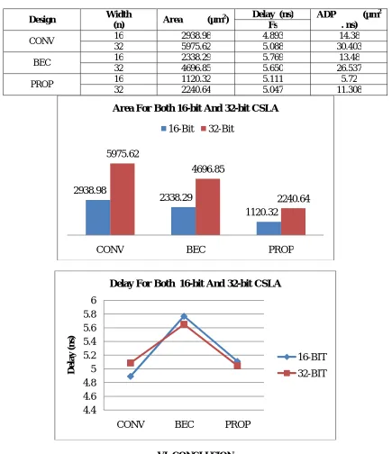
Table 2. Practical Estimate of Area and Delay of the Proposed and Existing 16 and 32-bit CSLA.
Design Width
(n) Area (µm
2
) Delay (ns) ADP (µm
2
. ns) Fs
CONV 16 2938.98 4.893 14.38 32 5975.62 5.088 30.403 BEC 16 2338.29 5.769 13.48
32 4696.85 5.650 26.537 PROP 16 1120.32 5.111 5.72
32 2240.64 5.047 11.308
VI. CONCLUSION
We have estimated the logic function occupied in the conventional and BEC-based CSLAs to study the datadependence and to identify unneeded logic operations. We have eliminated all the unneeded logic operations of theconventional CSLA and proposed a new logic formulation for the CSLA. In the expected design, the carryselect (CS) function is planned before the calculation of final-sum, which is different from the conventionalapproach. Carry words equivalent to input-carry ‘0’ and ‘1’ generated by the CSLA based on the proposedmethod follow a specific bit pattern, which is
2938.98
2338.29
1120.32 5975.62
4696.85
2240.64
CONV BEC PROP
Area For Both 16-bit And 32-bit CSLA
16-Bit 32-Bit
4.4 4.6 4.8 5 5.2 5.4 5.6 5.8 6
CONV BEC PROP
D
e
lay
(n
s)
Delay For Both 16-bit And 32-bit CSLA
16-BIT
ISSN(Online): 2319-8753
ISSN (Print): 2347-6710
I
nternational
J
ournal of
I
nnovative
R
esearch in
S
cience,
E
ngineering and
T
echnology
(An ISO 3297: 2007 Certified Organization)
Vol. 6, Special Issue 11, May 2017
used for logic optimization of the CS unit. Fixed input bits of theCG unit are also used for logic optimization. Based on this, an optimized design for CS and CG units areobtained. By these optimized logic units, an efficient design is obtained for the CSLA. The proposed CSLAdesigns engage significantly less area and delay than the recently proposed BEC-based carry select adder. Dueto the small carry output delay, the estimated CSLA design is an excellent nominee for the SQRT adder. TheFPGA synthesis result shows that the existing BEC-based SQRT-CSLA design involves more area delayproduct than the proposed SQRT-CSLA, for different bit-widths.
REFERENCES
[1] O. J. Bedrij, “Carry-select adder,” IRE Trans. Electron. Comput.,pp. 340–344, 1962.
[2] J.Sklansky, “Conditional-Sum Addition Logic,” IRE Trans. Electron. Comput.,vol. EC-9, pp.226-231, 1960.
[3] T. Y. Ceiang and M. J. Hsiao, “Carry-select adder using single ripple carry adder,” Electron. Lett., vol. 34, no. 22, pp. 2101–2103, Oct. 1998. [4] Y. Kim and L.-S. Kim, “64-bit carry-select adder with reduced area, “Electron. Lett., vol. 37, no. 10, pp. 614–615, May 2001.
[5] M.Alioto et.al, “A Gate Level Strategy To Design Carry Select Adders,” ISCAS 2004.
[6] BehnamAmelifard et.al “Closing the Gap between Carry Select Adder and Ripple Carry Adder,” Proceedings of the Sixth International Symposium on Quality Electronic Design (ISQED’05), 2005.
[7] Y. He, C. H. Chang, and J. Gu, “An area-efficient 64-bit square root carry select adder for low power application,” in Proc. IEEE Int. Symp.CircuitsSyst., 2005, vol. 4, pp. 4082–4085.
[8] B. Ramkumar, H.M. Kittur, and P. M. Kannan, “ASIC Implementation Of Modified Faster Carry Save Adder,” Eur. J. Sci.Res., vol. 42, no. 1, pp. 53–58, 2010.
[9] B. Ramkumar and H.M. Kittur, “Low-power and area-efficient carry-select adder,” IEEE Trans. Very Large Scale Integr. (VLSI) Syst., vol. 20, no. 2,pp. 371–375, Feb. 2012.
[10] I.-C. Wey, C.-C. Ho, Y.-S. Lin, and C. C. Peng, “An area-efficient carry select adder design by sharing the common Boolean logic term,” in Proc.IMECS, 2012, pp. 1–4.
[11] S.Manju and V. Sornagopal, “An efficient SQRT architecture of carry select adder design by common Boolean logic,” in Proc. VLSI ICEVENT, 2013,pp. 1–5.