ABSTRACT
HAN, YIWEI. High-Resolution Electrohydrodynamic (EHD) 3D Printing of Function Materials (Under the direction of Dr. Jingyan Dong)
This study focuses on developing high-resolution printing processes for multi-functional materials. First, we investigated a high-resolution EHD printing technology for the fabrication of micro-scale 3D structures with phase change ink. A series of experiments have been performed to characterize the EHD printing process. In this study, the droplet size and droplet printing frequency can be directly determined by the applied voltage. For a better controlling of the printing frequency and droplet size, a DC pulse voltage based printing process was developed and characterized. We also characterized the printing process using AC voltage, which allows neutralizing the charges on the droplets and will benefit high-resolution 3D printing especially with conductive material on insulating substrates. After finding the optimal parameters for the e-jet printing, a few 3D structures were directly fabricated with good quality and high-resolution.
To understand the mechanism of the drop-on-demand EHD printing, FEA-based
In the traditional EHD printing system, a substrate is placed between the ground electrode and the printing nozzle, which limits the maximum height of the printed structures. In order to have substrate independent printing, a ring electrode was designed and fabricated in this study. The ring electrode has a circular hole in the middle of a thin glass slide coated with conductive material. This grounded ring electrode was integrated into the printing nozzle that free the ground electrode under the substrate in the traditional printing system. FEA simulations were performed to find the best design parameters that can provide the enough electric field to start EHD printing. With the help of the FEA model, the best design parameters can be found, and with this new electrode design, high-resolution 3D structures with large aspect ratio can be fabricated.
Lastly, this study investigated high-resolution EHD fabrication of flexible and stretchable conductors with two advanced materials. The first material is low melting point metal alloy. A high-resolution EHD printing process was developed and characterized for the molten metal, which was capable of producing metallic features with a sub-50µm resolution. High-resolution 2D patterns and 3D structures have been printed to demonstrate the printing capability for flexible and stretchable electronics. Bending test and stretching test of the printed conductors showed the excellent performance on the flexibility and stretchability. A high-resolution and high-density capacitance sensor has been successfully printed and tested. An FEA model was created to simulate the behavior of the capacitance sensor. The second material is one
showed excellent performance in both flexibility and stretchability. Two wearable devices were fabricated and tested to demonstrate the potential application of this EHD printing technique for AgNW based flexible and stretchable devices.
High-Resolution Electrohydrodynamic (EHD) 3D Printing of Function Materials
by Yiwei Han
A dissertation submitted to the Graduate Faculty of North Carolina State University
in partial fulfillment of the requirements for the degree of
Doctor of Philosophy
Industrial and Systems Engineering
Raleigh, North Carolina 2018
APPROVED BY:
_______________________________ _______________________________ Jingyan Dong Paul Cohen
Committee Chair
DEDICATION To my family
BIOGRAPHY
ACKNOWLEDGMENTS
First of all, I would like to express my most profound appreciation to my advisor, Prof. Jingyan Dong for his knowledge, guidance, and support in the last five years. I also would like to express my gratitude to my committee, Prof. Paul Cohen, Prof. Yuan-shin Lee, and Prof. Yong Zhu for their valuable thoughts and feedback. In addition, I would like to thank Prof. Mohamed Bourham for taking the role of Graduate School representative on my committee.
TABLE OF CONTENTS
LIST OF TABLES ... vii
LIST OF FIGURES ... viii
CHAPTER 1 INTRODUCTION ... 1
1.1 Motivation ... 1
1.2 Research Objectives and Scope ... 4
1.3 Dissertation Outline ... 8
1.4 Chapter Summary ... 8
CHAPTER 2 LITERATURE REVIEW ... 9
2.1 Overview of Traditional Additive Manufacturing ... 9
2.1.1 Liquid Based Additive Manufacturing ... 9
2.1.2 Solid Based Additive Manufacturing ... 13
2.1.3 Powder Based Additive Manufacturing ... 14
2.2 Overview of Current Printing Technologies ... 19
2.2.1 Inkjet Printing ... 20
2.2.2 EHD Printing ... 21
2.2.3 pyroelectrodynamic printing ... 21
2.2.4 Saw Printing... 22
2.2.5 Screen Printing ... 23
2.2.6 Offset Printing ... 24
2.2.7 Gravure Printing ... 25
2.3 Overview of EHD Printing Technology ... 26
2.4 Chapter Summary ... 31
CHAPTER 3 HIGH-RESOLUTION EHD 3D STRUCTURE PRINTING ... 32
3.1 EHD 3D Printing System and Material ... 32
3.1.1 Printing Material ... 32
3.1.2 Printing System ... 33
3.1.3 Pattern Characterization ... 35
3.2 EHD Printing Processes and Characterization Under Continous DC voltage ... 36
3.3 EHD Printing Process Under Controlled Voltage ... 39
3.3.1 EHD printing process under DC pulsed voltage ... 39
3.3.2 EHD printing process under AC voltage ... 46
3.4 EHD 3D Structures Printing ... 50
3.5 Chapter Summary ... 53
CHAPTER 4 MODELING OF EHD 3D PRINTING PROCESS ... 55
4.1 Modeling for Droplet Formation ... 55
4.2 Modeling for Droplet In-Flight Velocity ... 55
4.3 Modeling of Droplet Settlement on Substrate ... 65
4.4 Modeling Results of EHD Printing ... 67
4. 5 Chapter Summary ... 70
CHAPTER 5 Ring Electrode Design for EHD Printing ... 71
5. 1 EHD 3D Printing System with Ring Electrode ... 71
5.1.2 Printing Material ... 72
5. 2 Ring Electrode Design ... 72
5. 3 FEA Modeling of Ring Electrode Design ... 75
5.4 Characterization of Ring Electrode Design ... 82
5.4.1 Verification of Ring Extractor Design ... 82
5.4.2 Characterization of EHD printing using Ring Extractor ... 85
5.5 EHD Filament Printing of 3D Structures ... 89
5. 6 Chapter Summary ... 90
Chapter 6 EHD printing of electronics with advanced materials ... 92
6.1 High-resolution EHD direct metal printing of electronics ... 93
6.1.1 printing system and printing material ... 93
6.1.2 EHD Metal printing process and characterization ... 95
6.1.3 Direct molten metal printing of 2D and 3D features ... 101
6.1.4 Direct Fabrication of Flexible and Stretchable Conductors ... 103
6.2 EHD printing of electronics with silver nanowire ... 114
6.2.1 EHD printing of AgNW... 114
6.2.2 Morphology and Electrical Properties of Printed AgNW ... 118
6.2.3 EHD Printing of AgNW Devices ... 123
6.3 Chapter Summer ... 125
CHAPTER 7 FUTURE WORK, SUMMARY AND TIMELINE ... 128
7.1 Research Summary ... 128
7.2 Future Work ... 131
LIST OF TABLES
LIST OF FIGURES
Figure 2.1 Principle of FDM process [44] ... 10
Figure 2.2 Schematic of polyjet 3D printing process [50] ... 11
Figure 2.3 Schemes of two types of stereolithography systems. (a) Laser-based (b) digital light projection.[54] ... 12
Figure 2.4 (a) Mechanism of the LOM machine. (b)LOM building process. [70] ... 13
Figure 2.5 3D printing process: 1 and 2 place a layer of powder. 3 Binder is printing to this powder layer. 4 The whole will be repeated for every layer [73] ... 14
Figure 2.6 Schematic of LENS system setup [77] ... 16
Figure 2.7 Schematic of EBM system setup [82] ... 17
Figure 2.8 Schematic overview of SLS system [90]. ... 18
Figure 2.9 Schematic of SLM system setup [96] ... 19
Figure 2.10 Schematic of drop on demand inkjet printing [97]. ... 20
Figure 2.11 (a) Schematic of the pyroelectrodynamic printing system, including two plates and a heat source. (b) Droplet deposited onto substrate.[106] ... 22
Figure 2.12 Schematic of nanoscale wave propagation and atomization [108]. ... 23
Figure 2.13 Schematic of the screen printing process [111]. ... 24
Figure 2.14 Schematic of the offset printing process [111]. ... 25
Figure 2.15 Schematic of the gravure printing process [112] ... 25
Figure 2.16 EHD printing system set-up [7]. ... 28
Figure 3.1 Schematic of the EHD printing set-up... 33
Figure 3.2 (a) interchangeable nozzle base (b) Nozzle glued with base (c) Syringe ... 35
Figure 3.3 (a) Cone-shape at initial start voltage under pulsation mode (b) Printed larger size droplet at initial start voltage. (Scale bar 50μm) ... 37
Figure 3.5 (a) Printed satellite droplets (b) Multi-jet in EHD printing. Scale bar: 100
µm. ... 39 Figure 3.6 The regular DC pulsed voltage signal ... 40 Figure 3.7 The result of printed droplet under pulsed DC voltage with different voltage
amplitudes; (scale bar: 50 μm) ... 41 Figure 3.8 The result of printed droplet under pulsed DC voltage with different duty
cycles (scale bar: 50 μm) ... 42 Figure 3.9 The result of printed droplet under pulsed DC voltage with different pulse
frequencies. (Scale bar: 25 μm) ... 43 Figure 3.10 Different combinations of voltage and duty cycle for a printing frequency of
50Hz. (scale bar: 50 μm) ... 44 Figure 3.11 (a) The modified DC pulsed voltage signal (b) 50Hz of printing frequency
under voltage of 1250V (scale bar: 50 μm) ... 45 Figure 3.12 (a) Square AC voltage signal pattern (b) generated square AC voltage in
function generator. ... 47 Figure 3.13 Printing result under different AC voltage frequency (Scale bar: 50 μm) ... 48 Figure 3.14 Printed droplet under continuous DC voltage of (a) 900V and (b) - 900V. ... 49 Figure 3.15 Printed droplet under different duty cycle (a) 60% positive voltage and 40%
negative voltage (b) 70% positive voltage and 30% negative voltage. ... 50 Figure 3.16 Micro-structures printed from EHD printing process (a) pyramid (b) Single
layer wall (c) Rectangle tube (d,e) circular tube with thin walls. (f) Close
view of a single pillar (g,h ) Micro-pillar array matrix (i) 3D letter of NCSU. ... 51 Figure 4.1 Schematic configuration for FEA modeling of the electrostatic force and
surface tension on the droplet. ... 57 Figure 4.2 (a) The created model for the simulation (b) and (c) The zoomed in picture
around the nozzle tip. ... 58 Figure 4.3 The model after applying voltage load to the nozzle and bottom surface of
the substrate. ... 59 Figure 4.4 (a) The picture of the model after solved. (b) and (c) The electric field
distribution round the meniscus. (d) Electric field intensity around the
Figure 4.5 FEA model of droplet in-flight between tip and substrate. ... 62 Figure 4.6 (a) Electric field distribution along center axis. (b) The amount of charge of
droplet under different voltages. (c) Droplet velocity under different voltage and different flight time (d) Droplet impact velocity with different printing
voltages. ... 63 Figure 4.7 Modeling of the four stages (a) Initial statue of droplet impact (b) Droplet
impact on substrate. c) Droplet spreading on substrate surface. d) Droplet
settlement and solidification. ... 66 Figure 4.8 (a) In-flight droplet before impact the substrate. (b) Initial impact of the
droplet on substrate. (c) Droplet spreading on substrate surface. (d) Droplet
settlement and solidification. ... 68 Figure 4.9 Comparison between droplets height (a) and diameter (b) from FEA (lines)
and experimentally measured results (data points) at different process conditions. (c) Experimentally measured droplet cross section on substrate.
(Unit of x and y coordinates is μm, and measurement is shown as red line). ... 69 Figure 5.1 Schematic of EHD printing system with a ring extractor... 72 Figure 5.2 (a) Schematic of ring extractor design. (b) Ring extractor and tip picture that
taken from experiment camera. ... 73 Figure 5.3 (a) Microscope cover glass (b) Vertical view of the cover glass ... 74 Figure 5.4 Schematic configuration for FEA modeling of the electrostatic force on
droplets. ... 76 Figure 5.5 (a) Electric field potential distribution (b) electric field strength around the
printing tip of non-extractor at 825v with a standoff of 150 μm (unit of the
scale bar is V/μm). ... 77 Figure 5.6 (a) (b) FEA model of the cross-section of the nozzle, ring extractor, ejected
material and substrate. (c) Electric field strength around the printing tip at
1600V (unit of the scale bar is V/μm). ... 78 Figure 5.7 The relationships between the electric field strength and (a) standoff height,
(b) ring diameter, and (c) tip to ring extractor z-distance. ... 80 Figure 5.8 The printing behavior at the nozzle tip (a) without ring-extractor at 1s, 7s,
and 20s, and (b) with ring-extractor at 1s, 3.5s, and 9s. ... 83 Figure 5.9 Printed filaments at different voltage from 1400v to 1800v (scale bar: 100
Figure 5.10 Printed filaments under different printing speed from 10mm/s to 20mm/s
(Scale bar: 100 µm) ... 88 Figure 5.11 EHD filament printing of 3D microstructures. (a) Thin wall structure with a
tilt angle of 45 degree. (b) Thin wall structure with a tilt angle of 80 degree. (c) Thin wall structure from top view. (d) Ring structure. (e) Square corner.
(f) Top view of a square corner. ... 90 Figure 6.1 Schematic of EHD printing system ... 93 Figure 6.2 (a) large droplet of molten metal ink extruded under a pressure of 5 psi at the
nozzle tip. (b) Optical image of the pneumatically extruded metal filaments at printing speed of 20, 25, 30, 35, 40, 45, 50mm/s respectively from top to
bottom with a constant pressure of 10 psi. Scale bar: 5mm ... 95 Figure 6.3 (a) EHD printing behavior around the nozzle (b) EHD printed metallic
filaments on glass at different voltage of 500, 1500, 1600, 1700, 1800, 1900, 2000V respectively from top to bottom. (c) Printed metallic filaments on glass substrate at printing speeds pf 0.5, 1, 1.5, 2, 3, 4mm/s respectively from top to bottom (d) Line width of the EHD printed filaments as a function of the printing voltage at constant printing speed of 0.5mm/s. (e) Line width of the EHD printed filaments as a function of the printing speed at a constant
voltage of 1900V. Scale bar: 500µm. ... 97 Figure 6.4 (a) to (c) EHD printed patterns from Field’s metal, Wood’s metal and solder
on different substrates (from left to right: microscope glass slide, PDMS, PET, photo paper) (d) Contact angle for different materials on different substrates. (e) Contact angle between Field’s metal and PDMS substrate.
Scale bar: 5mm ... 100 Figure 6.5 (a) EHD printed high-resolution 2D patterns (b) Vertical metal wire (c)
Metal bridge structure. (d) Thin wall. Scale bar: 500µm ... 102 Figure 6.6 (a) EHD printed conductor on PDMS with a Christmas tree pattern that
connected a battery to light a LED (Sale bar: 500µm). (b) The conductor remained conductive at the bending state. (c) Resistance of the Christmas tree conductor as a function of bending diameter. (d) Resistance of the Christmas tree conductor as a function of the number of bending tests at the
bending diameter of 10mm and 5mm. ... 104 Figure 6.7 (a) Optical image of printed different designed conductor pattern (from top
to bottom: a straight-line, Half-circle, and horseshoe.) (b) Resistance changes as a function of tensile strain (0-70%) for three different designed pattern. (c) Optical image of a metallic conductor with horseshoe pattern under tensile strains of 0%, 25%, 50%. (d) Resistance as a function of tensile strain
Figure 6.8 (a) and (b) Printed feature before and after healing process (c) Optical image of break point in the printed feature before and after healing. (e) Bended feature after healing process (f) Horseshoe pattern on stretching test table (g) and (h) optical image o break point in half circle pattern before and after healing (i) Resistance as function of tensile strain in the initial to third time
of healing process. ... 108 Figure 6.9 (a) schematic of printed touch sensor. (b) Working principle of touch sensor
matrix. (c) Optical images and SEM image of a 20x20 touch sensor array and compared with a one cent coin. (d) A microcontroller board (ARDUINO MEGA 2560) was used to map the signal from 4x4 touch sensors array to a 4x4 LED matrix. (e)The change of the capacitance when touch point under
different sampling point. (f) and (g) Activated LED on point 1 and point 2. ... 111 Figure. 6.10 (a) FEA model for touch sensor design. (b) Cross section of electric potential
of touch sensor with and without a touch pen (c)Simulation result of the changing capacitance (ΔC) of points when the touch pen touch red
point(point 1) (unit: pF). ... 113 Figure 6.11 (a) and (b) Printing behavior for extrusion printing and EHD printing. Scale
bar: 150µm. (c) Three different high-resolution AgNW patterns. (d)
Large-scale AgNW pattern printed by EHD method. Scale bar: 5mm. ... 116 Figure 6.12 (a) and (b) Printed line width as a function of printing speed
and stand-off. (c) Optical image shows the clean and smooth edge. Scale bar: 50µm ... 117 Figure 6.13 AgNW alignment at edge and center of the printed line with a printing of (a)
10mm/s and (b) 1mm/s. Scale bar: 10µm ... 118 Figure 6.14 (a) The resistance of printed AgNW lines with different line widths. (b) The
conductivity of the printed AgNW lines with different line widths. ... 120 Figure 6.15 Optical image of printed AgNW lines on various substrates. (a)(a) Printed on
a variety of substrates (a) letter paper, (b) glass, (c) PET, (d) nanofiber paper, (f) PDMS and (f) polycarbonate filter. ... 121 Figure 6.16 (a) Optical image of bending test of bending angle from 0° to 180°. (b)
Resistance of printed AgNW pattern under different bending curvature. (c) Resistance under 200 bending cycles with a bending curvature of 0.37
(bending radius 2.7mm). (d) Resistance as a function of different strain under different stretching and releasing cycle. (f) Resistance under 300 cycles of
stretching and releasing ... 122 Figure 6.17 (a) IR image of printed AgNW heater under activated/de-activated condition.
Figure 6.18 (a) Printed dry ECG on PDMS film. Scale bar: 5mm. (b) ECG signals collected from the AgNW dry ECG electrode and a commercial 3M wet
CHAPTER 1 INTRODUCTION 1.1 MOTIVATION
Additive manufacturing [1-5] has the capability for rapid prototyping and small volume production of components for many applications such as aerospace, medical device fabrication, electronic device fabrication and automotive industries. Most of the existing additive processes, including selective laser sinter (SLS), electron beam melting (EBM), stereolithography, 3D printing, and fused deposition modeling (FDM) have the best resolution of no better than 50µm, and the improvements of their resolutions are usually very challengeing. For example, for laser or electron beam based additive manufacturing, the resolution is limited by the beam or laser spot size; for extrusion-based additive manufacturing, the resolution is limited by the nozzle size; for particle-based technology, the used particle size will limit the fabrication resolution, and in order to improve those require large energy, high investment cost, high material requirement, high pressure, etc.
High-resolution additive manufacturing is critical for many engineering applications. Lousy accuracy and surface finishing part will significantly limit the applications of the current additive manufacturing process in the production of high precision parts. The high-resolution 3D printing can provide high accuracy and quality surface finishing, which can effectively reduce the post-processing time and cost. High-resolution printing technology can also reduce the complexity of manufacturing process in many industrial areas such as aerospace, automotive, healthcare, etc. For instance, in the aerospace industry, with the high precision printing
printing allows printing the unique model for different patients without increasing any workload when compared with traditional manufacturing technologies. In the tissue engineering, the biocompatible scaffolds are crucial to support cell functions and regulate cell response to the scaffold such as cell alignment and cell contact guidance [6,7].
EHD printing [8-10] has been developed for several decades, and it is a high-resolution printing approach, in which the ink is subjected to the electric field to form a Taylor-cone and produce fine jet or droplet from the apex of the cone, thus to overcome the limitation from the nozzle size in tradition 3D printing. Drop-on-demand EHD printing with phase change ink has a unique advantage of quick solidification after printed on the substrate that would provide a promising process for micro-scale 3D structure fabrication. For other widely used aqueous or solvent-based inks, usually a small portion of functional materials can be preserved after solvent evaporation or post-process, which leads to a very low layer thickness of the printed feature. However, with phase-change ink, the printed layer will have a higher thickness about 1μm that usually hundred times larger than that using aqueous or solvent-based inks. The reason is that phase-changed ink will get solidified very quickly once it printed on the substrate; and with the short solidification time, limited ink spreading will also result in a higher thickness.
Currently, most of the EHD printing process are focused on the one dimension or two dimension printing, and only a few of the research has investigated the 3D EHD printing [11,12], so it is a great challenge to develop a 3D multi-materials EHD printing process that has the ability to printing arbitrary 3D structures. Though lots of efforts have been put into EHD
model should be created for EHD printing process, which can apply to more general printing conditions. For the traditional planar EHD print 3D structure, the process is becoming more and more difficult to control, and the height of printed parts is also limited because of the ground electrode is placed under the substrate, which makes this printing process not substrate independent. So a new printing system has to be developed for EHD printing, and this system can overcome the substrate effect and standoff distance (distance between the substrate and the nozzle), which can allow the system to print higher structure with better controllability and process stability.
Flexible and stretchable electronics are vital for the next generation electrical devices, but the materials used for printing electronics such as metal nanoparticles [13-15], conductivity polymers [16-18] and liquid metal [19-24] are either expensive or low conductivity or low resolutions. Moreover, most of the fabrication approaches for those materials need post-treatment, which increase the fabrication time and cost. Currently, only a few research
investigated direct writing of molten metal [14,25-27] for the fabrication of electronics but also with limited resolution. Since EHD printing has the potential to provide high-resolution and cost-effective printing, molten metallic materials can be applied to this method for fabrication of high-resolution and high conductivity flexible and stretchable electronics. Metallic nanowires is another advanced material for fabrication of flexible and stretchable electronics because a random network of nanowires can provide high conductivity and good flexibility and
the “rule of thumb,” the size of the particles in ink is suggested not to exceed 1/100 times of the nozzle size to prevent from nozzle clogging, the printed resolution is limited by the nozzle size. Since EHD printing does not require very small nozzle to produce high-resolution, it is an ideal technique for printing of AgNW based flexible and stretchable electronics. Few studies have investigated the EHD printing with metallic nanowires. However, they are focusing on the alignment of the NWs, which has a very low NWs density in ink and the printed lines are not conductivity.
This study is focused on developing a high-resolution EHD 3D printing process using polymeric and metallic materials; modeling of drop-on-demand EHD printing process and a new printing head model to simulate the EHD printing process; developing EHD printing process for the fabrication of high-resolution flexible and stretchable electronics. These research objectives and the scope of this research are discussed in the following section.
1.2 RESEARCH OBJECTIVES AND SCOPE
The broader objective of this dissertation is to develop a new printing method, which can provide high-resolution DoD printing; create a model that will give a hand to better understand the insight of the printing mechanism and process optimization; design a new printing head for substrate-independent printing; apply EHD technology to metal nanowire to fabricate high-resolution flexible and stretchable electronics; and high-high-resolution direct EHD printing of molten metal to fabricate 3D structure and electronics.
The specific objective of this dissertation proposals are as follows:
process will be performed for printing with different types of printing votlages, DC voltage, and AC voltage. In DC voltage characterization, two different types of voltage signal will be applied to the system. When using the regular DC voltage signal in printing, the characterization will focus on the influence of the voltage amplitude to the droplet size and droplet printing frequency. When using the DC pulsed voltage signal, three main parameters (voltage amplitude, pulse frequency, and duty cycle) will affect the droplet size and printing frequency, and each of those parameters will be charactered in the experiments. When using the DC voltage, the printed droplet will contain charges especially for printing on a highly insulating substrate. In order to reduce the charges, an AC voltage will be introduced for printing process. In the characterization process for using AC voltage, three parameters (voltage amplitude, frequency, and duty cycle) will be investigated for finding the relationship between those parameters and droplet size and ejection frequency.
Process models will be developed to simulate the overall EHD printing process that includes droplet formation around the meniscus, droplet inflight in the electric field between the nozzle and substrate, droplet impact and spreading on the substrate and final droplet
in-flight velocity is also simulated by FEA, and the simulated final droplet impact velocity will be used for the droplet impact and spreading phase. Droplet impact spreading and solidification will be simulated together, and the simulation results will be used to compare with the experiment results for validation. If the final experiment results have reasonable agreement with the
simulation result, which indicated that this printing model has the capability to predicate the final droplet size and shape.
For E-jet 3D printing, the most significant challenge is that the printing system is not substrate independent. The ground electrode is normally placed under the substrate. While building the structure layer by layer, the built structure will distort the electric field and cause an unstable printing condition because of the distorted field from the uneven surface. This will make the whole printing process difficult to control. In order to solve this problem, an integrated ring ground electrode will be designed for the printing system. The ring electrode will be
combined with the printing nozzle that will free the traditional planar ground electrode and make this printing system substrate independent so that the substrate and the printed structure will have zero or less effect to the printing system. The new printing head design will be first designed and studied using the FEA to find the optimal design parameters, and then the design will be
validated by experimental tests. If promising experimental results could obtain, which indicate that this design could overcome the dificulty of the traditional electrode setup, and improve the stability and controllability of the printing system effectively. 3D structures with high aspect ratio can also be fabricated with this integrated ring electrode design
production efficiency is low especially in large scale electronics traditional production. Directly metal printing can provide low cost with high fabrication efficiency. However, most of the printing technologies cannot provide high-resolution, which is not suitable to be used in micro-fabrication industry. Here, the EHD printing technologies will be applied to the molten metal ink. The overall printing process will be studied in the first place to find out the best combination of printing voltage, printing speed, temperature, back pressure, and standoff distance. Then 3D metallic structures will be fabricated to demonstrate the capability of EHD printing in 3D printing. Moreover, electronic devices will be produced to illustrate its ability to produce high-resolution micro-scale electronics using EHD printing technology. Bending, stretching, and self-healing test will be performed for the printed features to find their best performances.
A few groups have investigated the printing metal nanowires using EHD technology. However, the printed features with nanowires in the filament is not conductive because of the low density of the nanowire, which does not suitable for electronic fabrications. High-resolution printing will benefit micro-electronic industry in the aspect of reducing post-process, high conductivity features, and low cost. The material used in EHD printing is the solution that mixed silver nanowires and PEO solution. The different concentrations of the PEO will be first printed and charactered. Then, the different concentrations of AgNW will be mixed with the chosen concentration of PEO solution to find the optimal AgNW density. After obtained the value to AgNW density and PEO concentration, the characterization process will focus on the voltage amplitude, printing speed, and applied back pressure. With the optimal printing parameters, conductive features will be printed for bending and stretching test. Last, some high-resolution micro-scale electronics such as ECG and heater will be fabricated and tested for their
1.3 DISSERTATION OUTLINE
This dissertation proposal is composed of seven chapters. Chapter 2 is the literature review which includes traditional additive manufacturing, current printing technologies, and EHD printing technology. In the EHD printing review section, some limitations have been pointed out and which will be solved in this research. Chapter 3 first discussed the
characterization process for high-resolution EHD printing. The characterization includes printing process under both DC and AC voltage. Then the 3D structure printing process is discussed in the next part of chapter 3. In order to better understand the mechanism of the EHD printing, in chapter 4, an EHD printing model was developed for simulating of EHD printing process from droplet formation at the apex of the nozzle to the final droplet settlement on the substrate. The simulation results have a good match with the experimental results that indicate that this model can be used to predicate the droplet footprint under different given printing parameters. Chapter 5 presented an integrated designed of printing nozzle, which can overcome the substrate
limitation. The designed printing head was a substrate independent, which can improve the stability and controllability of the printing processes. The chapter 6 will discuss high-resolution EHD printing of molten metal and AgNW for fabrication of flexible and stretchable electronics. The chapter 7 will summarize the research and discussion about the expected research
contributions and some of the future works.
1.4 CHAPTER SUMMARY
This chapter discusses the research motivation of developing a new 3D printing
CHAPTER 2 LITERATURE REVIEW
This chapter began with literature reviews on traditional additive manufacturing. Some unique advantages and some limitations of traditional additive manufacturing such as
stereolithography, selective laser sintering (SLS), electron beam melting (EBM), 3D printing, etc. would be discussed in this chapter. The second section will discuss about current printing technologies, which include inkjet printing, screen printing, Electrohydrodynamic (EHD)
printing, etc. As one of the high –resolution printing methods, EHD printing will be discussed in the third part of this chapter, which included some backgrounds, developments, current research and some critical issues need to be solved.
2.1 OVERVIEW OF TRADITIONAL ADDITIVE MANUFACTURING
Additive manufacturing has been developed for over 30 years, and it is one of the best technologies for producing small volume parts and rapid prototyping for many applications. The major advantage of this technology is the reduction of the time and cost [40]. Many different kinds of traditional additive manufacturing technologies have been developed since the first time of this idea came up. Based on the material types, traditional additive manufacturing can be divided into three categories: liquid-based process, solid-based process, and powder-based process [41].
2.1.1 Liquid Based Additive Manufacturing
In the FDM process, usually, a thin filament of thermoplastic polymer feeds into a machine, where a temperature controlled extruder will semi-melt the material and force the material out from the extruder, and deposited the material onto the desired position on the substrate layer by layer [42,43]. The substrate will be lowered, or the printing nozzle will be lifted when a layer is finished and start to print next layer. The printing path and other parameters such as extruder moving speed, temperature setting, fill-gap, hatch pattern, strand-strand distance and layer thickness will be determined by the material used, required mechanical properties, part requirements and the application. Based on the shape of the final part, post-processing will be selected to perform accordingly. Figure 2.1 shows the scheme of FDM process [44]. The material used in this process are acrylonitrile butadiene styrene (ABS), polycarbonate (PC), PC-ABS blends, PC-ISO (medical grade PC), and polyphenylsulfone (PPSF) [43,45,46]. Another
type of the materials, for example, the thermoset polymers are difficult to be used in this technology, because they need curing process to solidify and form a structure once they
deposited on the substrate. The advantage of this technology is that no chemical post-processing required and cost-effective [47,48]. The main disadvantage of the FDM is that the typical
resolution is not high enough to produce high precision parts for many applications, the common resolution of this process is greater than 100 micros, because the material is extruded from the nozzle, the produced jet size is larger than the nozzle size. When reducing the nozzle size, the required pressure is increasing rapidly, which usually difficult to obtain. Another reason is that it requires high accuracy flow delivery and temperature control system, and this will tremendously increase the system cost.
Polyjet is an additive manufacturing process using inkjet technology to printing parts. The printing nozzle will move on the X and Y axis, and the printed material will be cured by the UV light, which the light is acted as a catalyst after finished each layer [49]. Figure 2.2 gives a schematic view of polyjet printing process [50]. The best layer thickness of the technology is
about 20 microns, but the X-Y resolution is still around 200 microns, and the mechanical properties are weaker due to the properties of the materials [51,52].
For stereolithography technology [41,53], the liquid photosensitive polymer will be placed in the ink bed, and a UV light will cure the material cross-section by cross-section. A platform will be used during the printing if some overhanging structures are designed. Once the overhanging layer is finished, the platform will be lowered down. Figure 2.3 shows the schemes for two type of stereolithography system [54]. Currently, many different low-molecular weights, multi-functional monomers, highly cross-linked materials have been used in this technology [55,56], and many more advanced materials have also been developed in recent years, such as liquid crystalline polymers [57-59] which have high stiffness and thermal stability,
hydroxyapatite [54,60,61], ceramics [62-65], and some metals [66,67]. For those advanced materials, a VU-curable prepolymer, photoinitiator, and other additives have to be mix with those materials to form a suspension. Stereolithography can provide high-resolution, good surface finishing parts, but the two main limitations of this technology are the high requirement of the materials, and the difficulty improvement of the printing resolution, which is limited by the UV-light size. Some of the other disadvantages of this method are that sometimes a final
(a) (b)
piece will be overcured for the overhanging part and the scanned line shape due to the scanning process [68].
2.1.2 Solid Based Additive Manufacturing
Laminated object manufacturing (LOM) process is a solid based additive manufacturing process, which the laser beam will be used to cut the desired shape from the material with a sheet
Laser (a)
(b)
shape. Each layer will be stick together by applying heat activated plastic [69]. Figure 2.4 has shown the components and the mechanism of the LOM machine and the schemes of the LOM processes [70]. This process is a low cost, no deformation or phase change process, and also it does not require any supporting structures. This technology has the potential to build large parts with internal cavities when compared with other additive manufacturing method. The drawback of this process is that it cannot produce high-resolution parts due to the laser beam size, and this process will generate a large amount of waste material. The produced part will have a large shrinkage in exchange for better strength after the thermal post-process [40].
2.1.3 Powder Based Additive Manufacturing
3D printing, Laser Engineered Net Shaping (LENS), Electron Beam Melting (EBM), Selective Laser Sintering (SLS), and Selective Laser Melting are the most common used powder-based additive manufacturing technology.
3D printing is an inkjet-based process, which the water-based liquid binder will be
printed from the nozzle onto a starch-based powder bed during the printing process. The powders in the powder bed stick together when the liquid binder is deposited on the bed [71]. The
structure will be built layer by layer by lowing the powder bed, and a fresh layer of powder is spread over the previous layers [72]. Once the final part is finished, post-processing is required to wash away the residue. Figure 2.5 shows the printing sequences of this printing process [73]. This printing technology has the capability to be used for a variety of materials such as metal, shape memory alloy (SMA), polymers, and ceramic [69,74-76]. This process does not require support material, because 3D printing uses powder as a substrate in each layer. However, the drawbacks of this process are inadequate surface quality, limited printed feature size, and porosity. Due to the almost identical printing process as inkjet, the jetted droplet size is directly determined by the nozzle size, and currently it very difficult to improve the nozzle size to obtain a better droplet size for a higher resolution. Also, once the droplet is deposited on the powder bed, the wetting of the droplet will reduce the resolution.
Laser Engineered Net Shaping (LENS), which the schematic of system setup is shown in Figure 2.6 [77], is an additive manufacturing process that a part is fabricated by melting metallic powder, which the powder is injected into a specific location. A high-powered laser beam will be used to melt the powder. The material will get solidified when it cooled down to form the
problems of this process is that the residual stresses by uneven heating and cooling processes will be significant in high precision processes.
In EBM process, a heated tungsten filament emits electrons, which are collimated and accelerated to a very high kinetic energy level, and this electron laser beam will be used as a heating source to melt or fused the powder [81]. The electron beam will first scan over the powder layer with a predefined pattern and consolidates the desired areas into solid and dense metals. Then the laser beam will preheat powders to a sintered state with fast scanning on the powder bed. During the melting or fusing process, the laser beam will scan the powder bed at a very low speed for each layer. After finished the current layer, a new powder layer is laid on top, and the scanning process is repeated until final part are completed. Figure 2.7 shows a typical EBM system [82]. The process takes place in a high vacuum chamber and to avoid build-up of
electrical charges in powder, very low amount of helium gas is added to the chamber [83]. This process can be used for a variety of metal powders, such as aluminum alloys, niobium, nickel alloys, beryllium alloys, stool steel, etc [83-88]. Typically, this method is used for industrials like aerospace that require high precision manufacturing and doesn’t need large volume production. The advantages of using this process are that it can melt metal powder with a very high melting point which only a few additive manufacturing processes can achieve the same, and it also can produce very high precision parts. The drawbacks of this process are also very obvious. This process requires vacuum chamber, which will cost lots of money; and this is a laser-based process, which means it also requires large energy and the printing resolution will be limited by the laser spot size.
SLS is also a laser-based powder additive manufacturing process, in which a
high-temperature laser is used to sinter a layer of fine powder with the selected pattern. Once the layer is finished, a roller will spread fresh layers of powder on the top of the bed to create a new powder layer for the next laser sintering [89]. Figure 2.8 shows the consists of the SLS system [90]. When using fine powders to achieve high-resolution printing, a vacuum chamber has to be used in this process, because those fine powders will have higher reactivity against humidity and oxygen. Moreover, due to prevailing interparticle forces, layers of finer powders are very loose, and those fine powder will also easily get agglomerated [91,92]. Some unique methods [93] have to be performed to prevent the agglomeration, especially for the fresh powder layer. A variety of materials can be used in SLS, for example, plastics, metals ceramic and polymers [94,95]. The resolution of this process is usually larger than 500 micron for the commercial SLS system because the laser spot size is limited and also the limitation that comes from the powder size.
SLM process that shows in Figure 2.9 is very similar to SLS process [82], but the powder will be fully melted in the SLM process, which gives a chance to make much denser structure than the parts made by SLS [96]. Another advantage of SLM process than the SLS is that it can produce much more precision parts as high as 40 microns. However, this process requires much more energy and higher system cost than SLS.
2.2 OVERVIEW OF CURRENT PRINTING TECHNOLOGIES
Printing is a process that can reproduce text or images, and it is widely used in many areas such as manufacturing (food, prototyping, tooling), medical (pills, medical devices, bio-printing), industrial (apparel, automotive, aerospace), and sociocultural (art, communication, publication). This section will review someof the current printing technologies, which include
inkjet, EHD printing, pyroelectrodynamic printing, saw printing, screen printing, offset printing and gravure printing.
2.2.1 Inkjet Printing
There are two different printing mechanisms in inkjet printing, piezoelectric and thermal, and the scheme of inkjet printing is shown in Figure 2.10 [97]. Traditional inkjet printing use a binary operated electrostatic field to control the system to produce droplet [98], and usually, this kind of technology cannot provide high-resolution printing. However, some groups have
demonstrated an inkjet technology that can produce a droplet with a diameter of 5 microns. They bonded a thin piezoelectric annular disc to a thin edge clamped circular plate to eject a droplet.
By controlling the different frequency, droplets with different size will be produced. This technology can apply to many fluids and fine solid particles [99-101]. Currently, most of the inkjet is applied to print 2D pattern, only a few groups have demonstrated the capability of printing 3D structure by using inkjet [102,103], but higher system setup or material is required to achieve the 3D fabrication.
2.2.2 EHD Printing
In the EHD printing, the ink will subject in an electric field, and the mobile ions in the ink will generate a electrostatic force, which will drag ink out from the nozzle to produce droplet or jet. By relying on the electrostatic force, it can overcome the nozzle limitation and produce high-resolution structures. The detail of the EHD printing will be introduced in section 2.3. 2.2.3 pyroelectrodynamic printing
2.2.4 Saw Printing
The surface acoustic waves (SAW) printing [107] uses acoustic fields to drive the fluid’s movement, which generate nanometer scale (1-10nm) amplitude waves. The nanoscale wave will spread on the surface of the substrate that is made of elastic material. The energy from those waves will be confined to a depth of 3-4 times of the wavelength into the substrate, and finally,
(a)
(b)
other energy will be concentrated to a spot, which has a size equal to the wavelength of the radiation using focusing transducers [107]. Once the energy gathers around the spot, it can generate a large surface acceleration (~107 m/s2) that will distort the fluid-air interface, and then a single elongated column of liquid is produced. Figure 2.12 shows the schematic of this method [108]. With this technology, the best resolution can be archived is about 100nm when using nanoparticles [108,109]. The drawbacks of this printing method are that it cannot print free-form geometries, for example, text or pictures, which means it does not have the capability to produce 3D structures.
2.2.5 Screen Printing
The screen printing is developed back to the early of the 20th century. It is a versatile printing approach, which allows for full 2-dimensional patterning of the printed layer [110,111].
The main distinction from all other printing techniques is a large wet film thickness and a requirement for relatively high viscosity and low volatility of the ink. In the screen printing process, a squeegee will be forced into a screen that will bring it into contact with the substrate. Then the squeegee will go linearly across the whole screen and force the ink to go through the blank areas that in the screen onto the substrate to produce the desired pattern. Figure 2.13 shows the screen printing process [111]. The main advantage of this method is the unique visual result it can create. The ink used is very durable and can either print larger or small size pattern. The disadvantage of this process is that it requires multi-steps process (such as place screen and align) to finish the final product. Also, this method cannot provide a high-resolution printing,
2.2.6 Offset Printing
In the offset printing shows in Figure 2.14 [111], the ink image or roller is transferred to an image roller or plate that only the pattern area will be printed ink. The printed ink pattern will offset to a roller and transfer to the web. Usually, most of the process is water chemistry based, and the printed area is made of hydrophobic material, which can be easily wetted by the ink.
Offset printing is a fast process with relatively low cost on system and material [112].
2.2.7 Gravure Printing
Gravure printing directly transfers of inks through physical contact of the engraved structures to the substrate. This technology can provide a high-quality image with low system cost. The printing system consists of a giant roller electroplated with copper and engraved with
Figure 2.14 Schematic of the offset printing process [111].
micro cells that show in Figure 2.15 [112]. The microcells are fabricated by using either electromechanical or laser [113]. The cylinder is coated with a thin layer of chrome to protect from wear and tear during the printing process. Once the cells are filled with ink, a doctor blade is used for removing extra ink from the rotating roller. Ink will be transferred through capillary action onto the substrate, and Surface properties of the substrate will also be modified to assist the transferring process.
2.3 OVERVIEW OF EHD PRINTING TECHNOLOGY
EHD printing is a high-resolution printing technology, which has the ability to produce droplet or jet with a very high resolution that will overcome the nozzle size limitation. A Typical EHD printing system is displayed in Figure 2.16 [7]. Compare with the thermal or piezoelectric printing it will be easier to drag ink out from the nozzle using electrostatic force rather than applying high pressure. In the EHD printing, a voltage will be applied between the nozzle and ground electrode, which will generate an electric field around the nozzle. This electric field will accumulate the mobile ions in the ink to gather around the surface of the meniscus. With the Coulombic repulsion, a cone shape that also named as Taylor Cone will form at the apex of the nozzle [114]. When the electric field reaches a sufficient level, the electrostatic force will
overcome the surface tension, and small dimension droplets or jet will be ejected from the Taylor cone. Currently, a variety of materials such as polymers, nanoparticles, biomaterials have been successfully used in EHD printing [6,115-117], and printing resolution can reach to a few
microns or nanoscale. EHD printing process depends on many different parameters (e.g., applied voltage, printing speed, standoff distance, ink viscous, ink surface tension, etc.). Different
printing parameters will bring different EHD printing modes [114,118-124], such as
3D printing because it is very difficult to control the printing process to printing desired pattern. For example, during the electrospinning, the printed fiber on the substrate is usually random because of whipping behavior (bending instability). This unstable printing behavior is caused by the evaporating of the solvent in the printing ink, which is essential to the electrospinning. For electrospray, the electrostatic force will break jet into numerous tiny droplets. Although this is an axis-symmetric process, the produced tiny droplets cannot be controlled, which result in an unstable EHD printing. Those instabilities are necessary for those two printing modes, but for high-resolution EHD 3D printing, they are no longer have the capability to meet the requirement obviously. To achieve a high-resolution EHD 3D printing, very stable printing modes have to be used, which are EHD drop-on-demand printing [104,125-128] and EHD direct jet plotting [129,130]. In the drop-on-demand printing, a meniscus will be formed under the electrostatic force, and droplet will detach from the apex of the meniscus once the electrostatic force that applied on the droplet is large enough to overcome the surface tension force. In the direct jet plotting, due to the high viscosity of the ink, no droplet will detach from the apex of the
meniscus, the only fine filament will form at the apex of the meniscus and plot on the substrate when applying a proper voltage value to the system.
Drop-on-demand EHD printing with phase-change ink in pulsation mode can produce single tiny droplet each time, and this process has good controllability, which gives a potential to be used for high-resolution 3D structure printing. Many studies have already revealed the
information for the controlling of the printing process and predicting of printing behavior.
However, it is still very challenging to predict the droplet formation [104,125], in-flight size, and droplet footprint on the substrate under the different printing conditions. Computational
modeling based methods can provide promising result on the droplet formation in electrospray [132-136], but when dealing with the micro-scale droplet with high inflight velocity, this method is very difficult to be used for simulation or prediction for the EHD printing processes due to the highly complex coupled physics (electrostatic force, fluid dynamic, and singularity from the droplet pinch-off). Currently, there is no commercially available numerical solver that can successfully apply to the EHD drop-on-demand printing. Some of the groups [132-134]have developed their own solver to study some sub-set problems during the EHD printing processes. However, those solvers are very sophisticated and requiring high computational ability. Thus lots of computational load needs to be taken during the simulation. Few groups have created some highly simplified printing model to just provide the insight of this processes from engineering
perspective [133,137-139]. However, all of those models cannot simulate the overall printing process, so a model that can simulate the entire EHD printing processes that include droplet formation, droplet in-flight, and droplet settlement is remain.
EHD printing with phase-change ink has the capability to produce high-resolution 3D structures. Currently, most of the EHD printing systems have a planar ground electrode configuration, which the ground electrode is placed under the substrate. In this system setup, usually the applied voltage is a constant value during the printing, and the structures will be printed on the substrate. Once the ink is reached to the substrate, it will have some affections on the overall electric field distribution and intensity because the dielectric constant of the printing materials is different from that of the air. The effect of a single droplet or single layer is limited, and sometimes it can be neglected, but once the structure is building up, this influence cannot be ignored, and the electric field distribution and intensity will be changed extensively. Also, during the 3D printing, the height of the structure is limited by the distance between the printing nozzle and the substrate. For the traditional EHD printing system, the standoff distance is a constant value, which cannot allow the system to print higher structure. One of the methods to overcome this distance is to increase this standoff distance accordingly while printing. However, when lifting this z-direction, the electric field will be changed, and it is very challenging for process control to keep a constant electric field distribution and intensity due to the distortion effect of the electric field by the printed structure. Moreover, if higher structure needs to be printed, it will result in the large nozzle to substrate distance, and the required voltage will be very large, and this value is usually difficult to obtain.
generate the electrosprays for pollution filtration [140]. Mahoney’s research is using a plate ground electrode to generate ion source [141]. Some groups used pole integrated electrode to produce droplet [142,143]. The pole type nozzle will increase the efficiency of the jetting.
improve the stability and controllability of the printing processes. However, those studies only focus on the characterization phase of the designed electrode for the printing process, and a few groups have performed some experiment on the 1D (droplet or lines) and 2D patterns. The investigation of the influence of this ring electrode to the 3D structure printing is still unraveled.
2.4 CHAPTER SUMMARY
CHAPTER 3 HIGH-RESOLUTION EHD 3D PRINTING
High-resolution fabrication is very important for modern manufacturing. It can provide good surface finishing, high precision, and good mechanical properties. Traditional 3D printing technologies are very challenging of producing high-resolution structures due to many
limitations such as high energy required, high pressure required, laser or nozzle spot-size limitation, etc. In order to solve those problems, large amount money or energy has to be
invested into the system, which makes those systems very expensive. Even with some expensive equipment, it is also very challenging to improve some limitations, like laser size and nozzle size, so it will be difficult to fabricate high-resolution structures with traditional printing
technologies, which brings the high-resolution printing technologies to the front. In this chapter, a high-resolution printing technology (EHD printing) will be introduced, which has the
capability to produce structures with a sub-10µm resolution. The printing processes will be characterized using Direct Current (DC) and Alternate Current (AC) Pulsed voltage. Optimal parameters will be obtained after characterization process, and those parameters will be used for 3D structure printing.
3.1 EHD 3D PRINTING SYSTEM AND MATERIAL
3.1.1 Printing Material
mechanical strength. Phase-change materials also have a good corrosion resistance, and the cost is relatively low when compared with other printing materials. So this kind of material becomes very popular in the additive manufacturing. Commonly used phase changed ink in FDM include ABS, PLA, PC, etc. The paraffin wax belongs to phase-change inks, but it is seldom used in the additive manufacturing industry. The paraffin wax has a very low cost with the melting
temperature about 55 °C, which is very easy to melt it into the liquid phase, and this makes it a good candidate material for our EHD 3D printing,
3.1.2 Printing System
The EHD 3D printing platform consisted of four sub-systems: a three-axis (XYZ) precision stage, a thermal control system, a high voltage supply, and a pneumatic dispersion system. The precision stage was installed on an anti-vibration table to reduce vibrational noise, and three linear stages were installed to the precision stage in XYZ directions with repeatability and accuracy of 100nm, and the linear stage was used to move the printing nozzle and substrate to the programmed locations. This precision stage had a working envelope of 100 x 100 x 50mm.
Ground Electrode Substrate
Translational stage Voltage
supply
Heater Back Pressure
z-stage
The thermal control system consisted of three parts, a heating rope, which could provide a temperature up to 900°F (482 °C) for the printing syringe; a thermocouple was used to measure the heating temperature of the syringe; a proportional – integral – derivative (PID) controller was used to control the power of the heating rope. The heating rope was wrapped around the syringe to provide heat for the ink inside the syringe, and the thermocouple was inserted to the top of the syringe that was closed to the nozzle to measure the syringe temperature and provide temperature feedback to the thermal controller (PID). The entire thermal control system had a resolution of 0.5 °C. A function generator (Agilent 3220A) was used to generate a required voltage signal, and the signal was amplified by a voltage amplifier. The voltage amplifier (Trek Model 610E) was purchased from Trek, Inc., which could provide a maximum voltage of 10KV. The pneumatic dispersion system was used to provide the pressure for the EHD printing process and keep the required ink flow rate. The back pressure was provided by an air pump and controlled by a precision regulator, which would provide a maximum pressure of 6 psi. A high resolution (0.5μm) camera was used to monitor the printing processes.
the aluminum film was 50nm, and it was coated to the silicon wafer by using thermal evaporation. The substrate and the ground electrode were located on the XY-stage.
In this research, the 5ml syringe was purchased from CADENCE SCIENCE with a metal Luer lock. The syringe temperature was set to 110 °C, which would perfect melt the wax and also reduce the surface tension and viscosity of the melting wax. The printing precision core that was purchased from Subrex was made of nickel silver and has an ID of 51 μm and an orifice of 150 μm. The precision core was connected with an interchangeable nozzle base (Figure 3.2 (a)) that was purchased from Integrated Dispersion Solution, Inc. to form the printing head by using super glue (Figure 3.2 (b)), and then the printing head was screwed into syringe that shows in Figure 3.2 (c). In this study, the distance between the substrate and printing head was set to 150 μm.
3.1.3 Pattern Characterization
The filaments or micro-droplets will be printed on the substrate by using EHD printing method. The printed filaments or droplets was inspected under optical microscope, Atomic Force Microscopy (AFM) or Scanning Electron Microscope (SEM). The morphology of printed filaments or droplets and printed micro 3D structures were measured by using AFM or SEM.
Figure 3.2 (a) interchangeable nozzle base (b) Nozzle glued with base (c) Syringe
(a)
(b)
(c)
3.2 EHD PRINTING PROCESS AND CHARACTERIZATION UNDER CONTINOUS DC VOLTAGE
In EHD-jet printing, a large voltage was applied between substrate and printing head, which would gather mobile ions in the printing ink near the surface of the printing tip to form chargers. The charges would bring an electrostatic force to deform the meniscus at the tip of the nozzle to form a conical shape (Taylor cone). When increased the voltage, the electrostatic force will increase, which dragged more ink out from the nozzle to form a larger meniscus. When increased voltage to a certain intensity, the electric field was large enough to provide an electrostatic force at the apex of the cone that exceeded the surface tension force at the Taylor cone, a jet or a droplet would be injected from the meniscus onto the grounded substrate. Mostly, the plotting results will be affected by the fluid properties of the ink, printing process conditions (i.e., ink temperature, standoff distance), and applied printing voltage. In this study, only one material will be used during the characterization process, and the ink temperature and standoff distance will keep a constant value of 110 oC and 150μm. Small standoff distance makes it hard for us to observe the process and larger standoff will bring more disturbance during the printing process.
In this study, a positive voltage will be applied to the system, and only the value of this voltage will be changed during the characterization process. For melted wax in EHD printing, at the voltage of zero, no meniscus can be observed at the apex of the nozzle. When we gradually increased the printing voltage, a meniscus and Taylor cone was gradually forming at the tip of the nozzle, and due to the wetting of the printing material (wax), the diameter of the cone shape was equal to the orifice of the nozzle and only a small cone shape can be observed. When continuing increasing the voltage to a threshold value, the cone shape will increase (Figure 3.3 (a), and when the applied voltage was larger enough (around 650v in this system setup) to provide enough electrostatic force to overcome the surface tension, a micro droplet was ejected from the apex of the Taylor cone and printed onto the glass substrate. At this initial stage, the printed droplet that shows in Figure 3.3 (b) has a large diameter and the printing frequency was very low that can be explained as the following, at this initial voltage value, it required more mobile ions to provide enough electrostatic force to separate ink from Taylor-cone. More mobile ions mean it has to bring more volume of ink and longer charge migration waiting time for the mobile ions to gather around at the apex of the nozzle. When continuing increasing voltage, the cone shape will be further increased (Figure 3.4 (a)), because the larger electrostatic force will take out more ink from the nozzle. The droplet ejecting speed will increase, and the droplet size
(a)
(b)
will decrease. Figure 3.4 (b) has shown the droplet footprint size and printing frequency under different voltages from 850v to 1000v. It is obvious that increasing the voltage will lead to increase the printing frequency (from 5 Hz to 19Hz) but decrease the size of the printed droplets (from 17 μm to 8 μm), this can be easily explained by the mechanism of EHD printing. When increased the voltage, the surface charge density of the printing ink at Taylor cone would also be increased, so smaller volume of ink (smaller size of the droplet) will be needed to obtain large enough electrostatic force to overcome surface tension force and eject from the apex of the Taylor cone. Increasing the voltage will also increase the charge migration rate, which give a result of faster charge accumulation time at the apex of the cone to initiate ejection that will increase the printing frequency. Continuing increasing the voltage to a certain threshold, which 1500V in this study, satellite droplets or multi-jet which show in Figure 3.5 will be printed. Satellite droplets are very tiny droplets that occurre when the voltage is too high, because high voltage can provide high electrostatic force, which had the ability to shred droplet into several small droplets (satellite droplets), so the satellite droplet indicates unstable printing condition. High voltage will also split the meniscus to form multi emitting sites around the nozzle so that
Figure 3.4 (a) Cone shape at voltage of 850V. (b) Droplet size and printing frequency at different positive voltages (Droplet size from top to bottom: 17μm, 14μm, 11 μm, 8 μm)
100 μm
(a) (b) 850v
5 Hz 900v 7 Hz
multi-jet will be observed during the printing. Multi-jet mode usually has a higher flow rate but smaller droplet dimension when compared with pulsated mode printing.
3.3 EHD PRINTING PROCESS UNDER CONTROLLED VOLTAGE
3.3.1 EHD printing process under DC pulsed voltage
The voltage used in the experiments above is the DC voltage. The only controlling factor in the voltage is the value. From the last results, the droplet size and droplet jetting speed is directly determined by the applied voltage. The small voltage will result in a large droplet and slow jetting speed, and larger voltage will result in a small droplet and fast jetting speed. So, it is very difficult to obtain small droplet with a controllable jetting speeding when only apply
continuous DC voltage to the system. In the E-jet printing, a controlled printing frequency can bring many advantages, especially in 3D printing. During the 3D printing, a controllable printing speed can reduce many disturbances and deposit droplet more precisely. The DC pulsed voltage shows in Figure 3.6 will be controlled by three factors, amplitude of the voltage, duty cycle and
Figure 3.5(a) Printed satellite droplets (b) Multi-jet in EHD printing. Scale bar: 100 µm.
pulse frequency. The frequency will be used to control the droplet printing frequency, and voltage and duty cycle will match with each other to produce a droplet in a single cycle. To characterize the affection of those three factors to the printing process, we have to characterize one factor each time, and the printing frequency and droplet size will be used to verify the
printing process. The designed DC pulsed voltage wave pattern was created in the computer with Waveform Builder software. This signal will be sent to function generator and stored in the function generator. Once the function generator is on, it will send the pulsed voltage signal to the voltage amplifier, which will amplify the voltage to the required level, before sent to the printing system.
To study the effect of the voltage on the printing, the pulse frequency, and duty cycle will be fixed as 20Hz and 20%. Based on the characterization process in the previous section, when applying a continuous DC voltage of 1000V, the printed frequency is close to 20Hz. So choosing 20Hz will provide a relatively large voltage range that will allow us to perform the test because the start voltage is 650V and the highest voltage level is 1500V. Large duty cycle will easily generator two or more droplets in a cycle with a relatively low voltage, and a small duty cycle will be difficult for the system to generate single droplet in a cycle with a high voltage. So 20% duty cycle was chosen to ensure the easy observation and process control. The standoff distance
(a) Pulsed voltage
0 V
1 Cycle Duty Cycle
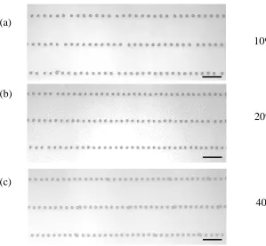
and stage moving speed for all printing will still keep as a constant of 150 μm and 1 mm/s. The result of the printed droplet is shown in Figure 3.7. Obviously, when the voltage is less than 1000V, no droplet with 20Hz frequency can be found. When the applied voltage is low (1150V in the Figure 3.7), there are some missing droplets on the substrate, which means during some cycles, no droplet is generated. At this time, the voltage is little insufficient, the electrostatic force generated during the pulse section cannot drag droplet out every time. When increasing the voltage to 1250V, the printed droplets have a printing frequency of 20Hz, which is match with the setting pulsed frequency. This time, the voltage reached a working level that can produce droplets with the desired frequency. Continuing increasing the voltage to a certain range, the printed droplet will keep a constant printing frequency of 20Hz. The increasing voltage will not lead to high printing frequency that is because the 20% duty cycle pulsed voltage does not have enough time to produce more than one droplet, which limited the number of generation of the droplet, which means the droplet printing frequency is under controlled. There is no obviously changing in droplet size, however, once the voltage exceeds a critical value (1450V in this
Figure 3.7 The result of printed droplet under pulsed DC voltage with different voltage amplitudes; (scale bar: 50 μm)
1150V
1250V
![Figure 2.1 Principle of FDM process [44]](https://thumb-us.123doks.com/thumbv2/123dok_us/1491688.1182535/27.612.159.445.373.678/figure-principle-of-fdm-process.webp)
![Figure 2.2 Schematic of polyjet 3D printing process [50]](https://thumb-us.123doks.com/thumbv2/123dok_us/1491688.1182535/28.612.161.459.467.679/figure-schematic-polyjet-d-printing-process.webp)
![Figure 2.4 (a) Mechanism of the LOM machine. (b)LOM building process. [70]](https://thumb-us.123doks.com/thumbv2/123dok_us/1491688.1182535/30.612.94.500.222.671/figure-mechanism-lom-machine-b-lom-building-process.webp)

![Figure 2.6 Schematic of LENS system setup [77]](https://thumb-us.123doks.com/thumbv2/123dok_us/1491688.1182535/33.612.177.443.73.368/figure-schematic-lens-setup.webp)
![Figure 2.7 Schematic of EBM system setup [82]](https://thumb-us.123doks.com/thumbv2/123dok_us/1491688.1182535/34.612.74.551.94.370/figure-schematic-ebm-setup.webp)
![Figure 2.8 Schematic overview of SLS system [90].](https://thumb-us.123doks.com/thumbv2/123dok_us/1491688.1182535/35.612.102.501.87.339/figure-schematic-overview-sls-system.webp)
![Figure 2.12 Schematic of nanoscale wave propagation and atomization [108].](https://thumb-us.123doks.com/thumbv2/123dok_us/1491688.1182535/40.612.121.456.304.554/figure-schematic-nanoscale-wave-propagation-atomization.webp)