Design and Implementation of Speech
Processing in Cochlear Implant
Pooja T 1, Dr. Priya E 2
P.G. Student (Embedded System Technologies), Department of Electronics and Communication Engineering,
Sri Sairam Engineering College, Chennai, Tamil Nadu, India1
Assistant Professor, Department of Electronics and Communication Engineering, Sri Sairam Engineering College,
Chennai, Tamil Nadu, India2
ABSTRACT: This paper represents the implementation of the speech processing phase of the cochlear implants which are among the great success technologies of modern medicine. This system is used by humans suffering from hearing impairment. In this work, the acoustic speech signal is made to pick up by the microphone and is amplified. The filter banks (I KHz to 6 KHz) is divided into three sub-bands. The appropriate speech signals are decoded by these sub-bands and are thus verified with the help of LEDs that are connected at the respective output of the sub-bands. The processed speech signals are given as input for the cochlear implantable unit. The cochlear implant is also known as a Bionic ear and the only medical technology existing for the sensorineural hearing loss.
KEYWORDS: Cochlear implant, Speech Processor, Bionic ear, Sensorineural hearing loss.
I. INTRODUCTION
Speech is man’s most important form of communication and the loss of hearing affects the communication process with respect to the spoken language. Scientists first attempted to restore normal hearing to the deaf by electrical stimulation of the auditory nerve. The first experiments were discouraging as the patients reported that speech was unintelligible. Today, a prosthetic device, called cochlear implant, can be implanted in the inner ear and can restore partial hearing to profoundly deaf people. Some individuals with implants can now communicate without lip-reading or signing, and some can communicate over the telephone as presented in dallasear.com [1].
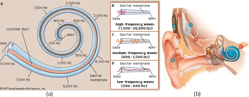
The human ear consists of three parts: (a) Outer ear: It simply funnels incoming speech pressure waves toward the eardrum, where these variations are transformed into mechanical vibrations. (b) Middle ear: The eardrum transfers power to the middle ear, which contains the ossicular bones: malleus, incus , and stapes. Among the smallest bones of the body, these three amplify eardrum vibrations and send them to the oval window membrane of the inner ear. The main amplification effect is due to a large difference in surface area: big eardrum versus small oval window.(c) Inner ear:It contains the cochlea, a very hard bony tube filled with lymphatic fluid. It converts mechanical vibrations of the oval window into electrical energy for its neural outputs. Approximately 30,000 sensory hair cells connect the basilar membrane to the auditory nerve, which leads to the brain. These cells lie in several rows along the length of the cochlea.
(a) (b)
Figure 1: (a) Spatial frequency arrangement of human cochlea, (b) CochlearImplant
If the hair-cell and auditory nerve damage is excessive, the connection between the central nervous system and the external world is lost and the person who has such level of loss is recognized as being profoundly deaf. Cochlear implants are designed to help severely to profoundly deaf adults and children who get little or no benefit from hearing aids. Even individual with severe or profound "nerve deafness" may be able to benefit from cochlear implants as specified in nidcd.nih.gov [2].
A typical cochlear implant device shown in Figure 1(b) consists of a speech processor, a behind-the-ear unit and a cochlear implant. Sound is picked up by a microphone in the behind the-ear unit and sent to the speech processor. Depending on the speech processing algorithm being implemented, the speech processor extracts various parameters from the input signal and determines the amplitude of the current pulses to be sent to the implant. The amplitude information is transmitted to a receiver/stimulator circuit implanted under the scalp of the patient. This circuit sends current pulses to the electrodes implanted in the cochlea of the patient. As a result, the auditory nerve is excited and transmits nerve pulses to the brainstem and brain, where they are interpreted as sound as specified in nidcd.nih.gov [2].
From the Figure 1(b), the sound processor (A) captures sound and converts it into digital code. The sound processor transmits the digitally coded sound through the coil (B) to the omplant (C) just under the skin. The implant converts the digitally coded sound to electrical signals and sends them along the electrode array, which is positioned in the cochlea. The implant’s electrodes stimulate the cochlea’s hearing nerve fibres, which relay the sound signals to the brain to produce hearing sensations.
II. RELATED WORK
III.METHODOLOGY
There are different speech processing strategies developed and are successfully in the cochlear implant like: (a) Continuous Interleaved Sampling(CIS)
(b) Compressed Analog and Simultaneous Analog Stimulation(SAS) strategy
(c) Multipeak strategy
(d) Spectral maxima sound processor
The spectral maxima sound processor (SMSP) was first successfully used in 1989. The processor includes sensitivity control, a microphone preamplifier, and a sound compressor followed by 16 band pass filters, full-wave rectifiers; low pass filters for analog signal processing. A scanning analog to- digital converter (ADC) is used to convert band signals into digital form with 8-bit resolution, and digitized signals are stored into a first-in first-out (FIFO) memory. Digitized spectral information is processed by a microprocessor and the maximum amplitude or amplitudes of the entire speech spectrum is determined. Depending on the external control parameter values, such as loudness and the implantee's stimulus threshold levels, and the position of the spectral maxima, the microprocessor transfers the electrode numbers with stimulus levels to the data encoder. The data encoder converts data frames into pulse streams and sends them to the RF transmitter as stated by Rane and Ram [5].
A) HARDWARE SYSTEM
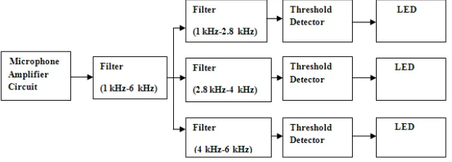
The proposed block diagram of hardware simulation of speech processor for cochlear implant is as follows:
Figure 2: Hardware System
In this system a microphone amplifier circuit, fourth order band-pass Butterworth filter (1 kHz-6 kHz), three filters, threshold detectors are used which helps to glow LEDs according to input sound signal. The basic function of microphone amplifier circuit is to amplify the input audio signal using condenser microphone. The amplified audio signal is given to fourth order band-pass Butterworth filter having cut off frequency of 1 kHz to 6 kHz, and is followed by bank of filters, threshold detectors and LEDs for analog signal processing. The 1 kHz-6 kHz frequency is divided into three sub-bands whose ranges are 1 kHz to 2.8 kHz, 2.8 kHz to 4 kHz and 4 kHz to 6 kHz using three fourth order band-pass Butterworth filters and outputs of those three filters are given to three LEDs through threshold detectors as presented in Rane and Ram [5].
MICROPHONE AMPLIFIER CIRCUIT: The microphone amplifier circuit is shown in Figure 3. The transducer
used in this circuit is the condenser type microphone.The entire circuit consumes a very small amount of power within the range of 10 mW. The voltage requirement of every major component is within the range of 1.8 volts and 15 volts. Therefore, for portability, a 3V DC battery is used to power the circuit.
amplifies the output of the pre-amplifier to an audible level. It comprises of the TDA2822M IC and those external components needed to make the IC function properly. A 32 ohms earphone is used in the output unit of this circuit as recommended by the manufacturers of the TDA2822M IC.
The aim of this circuit is to design a system that pre-amplifies an acoustic signal picked up by a condenser microphone. Capacitors C11 and C12 are called coupling capacitors. Their functions are to block any DC components in the input and outputs of the pre-amplifier.
Figure 3: Microphone amplifier circuit
The pre-amplifier comprises of R5 and capacitor C13 which decouples the power supply of the preamplifier stage, while capacitor C12 and resistors, R2, R3 and R4 with transistor T1 forms a negative feedback amplifier which stabilizes the overall gain. Resistor, R4 is known as an emitter swamping resistor which also adds stability to the amplifier as presented in Rane and Ram [5].
B) MATHEMATICAL ANALYSIS
A band-pass filter is a circuit which is designed to pass signals only in a certain band of frequencies while attenuating all signals outside this band. The parameters of a band-pass filter are the high and low cut-off frequencies, the bandwidth (BW), the centre frequency fc, and the selectivity. The key characteristic of Butterworth filter is that it has a flat passband as well as stopband. A band-pass filter has a passband between two cutoff frequencies fH and fL, where fH > fL and two stopbands 0<f<fL and f>fH. The bandwidth of the band-pass filter is, BW = fH – fL. ,fc is the centre frequency since it is approximately at the centre of the passband on stopband.
A band-pass filter has a centre frequency fc and is defined as √fHfL, where fH is high cutoff frequency (Hz) and fL is low cutoff frequency (Hz). A fourth order band-pass filter is formed by connecting in series or cascading second order high-pass filter and second order low pass filter. As the order of the filter increases, so does its size. Also the accuracy declines, in that the difference between the actual stop band response and the theoretical stop band response increases with an increase in the order of the filter. The overall gain of the filter is equal to the product of the individual voltage gains of the filter section. Any input frequency outside this passband is attenuated as proposed by Rane and Ram [5].
If the quality factor, Q<10 it is a Wide band-pass filter and if Q>10 it is a Narrow band-pass filter.
BW = fH – fL (2)
The rate at which the gain of the filter changes in the stopband is determined by the order of the filter. For second order low-pass filter the roll-off rate is 40 dB/decade, and by contrast the second order high pass filter the gain increases at the rate of 40 db/decade in the stopband , that is until f =fL. To obtain ±40 dB/decade band-pass, second order high-pass and second order low-pass sections are connected in series. Order of the band-pass filter depends on the order of the high-pass and low-pass filter section.
FILTER (1 KHZ-6 KHZ): Here fL=1 kHz and fH= 6 kHz and the component values are:
(a) C1=C2=C3= C4=0.0047 μF (b) R1=R1’= 27 kΩ, (c)R2=R3=33.804kΩ,
(d) R2’=R3’= 5.634 kΩ, (e) RF=RF’= 22 kΩ
Figure 4: Fourth Order Band-Pass Butterworth Filter (1 KHz- 6 KHz)
The above fourth order band-pass Butterworth filter is a combination of second order high pass Butterworth filter and second order low pass Butterworth filter.
BANK OF BAND-PASS FILTERS: All three filters that are used in the circuit are fourth order band-pass Butterworth
filters, designed in such a way that, these filters will divide frequency range 1 kHz- 6 kHz into 3 sub-bands .They are 1 kHz -- 2.8 kHz, 2.8 kHz -- 4 kHz and 4 kHz – 6 kHz.
SECOND ORDER HIGH PASS BUTTERWORTH FILTER FOR FREQUENCY BAND: The three sub-bands can
be implemented in the same circuit as depicted in Figure 4, but with the following Resistor and capacitor values varying depending on the low and high cut off frequencies. The values of components C1=C2=C3=C4= 0.0047 μF, R1=R1’=27 kΩ and RF=RF’=22 kΩ remain same for the three sub-bands and R2,R2’R3,R3’ varies for each sub-band. 1. For, Low Frequency=1 kHz and High Frequency= 2.8 kHz
(a) R2=R3= 33.804 kΩ (b) R2’=R3’= 12.093 kΩ
2. For, Low Frequency= 2.8 kHz and High Frequency= 4 kHz
(a) R2=R3= 12.093 kΩ (b) R2’=R3’= 8.465 kΩ
3. For, Low Frequency= 4 kHz and High Frequency= 6 kHz
(a) R2=R3= 8.465 kΩ (b) R2’=R3’= 5.634 kΩ
IV.RESULTS AND DISCUSSIONS
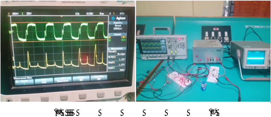
measured as 48mv. The top row of DSO presents the output of the microphone amplifier. This output was measured to be 1.07V.
(a) (b)
Figure 5: (a) Result of microphone amplifier circuit using DSO (b) Hardware setup and the output of the Butterworth filter
The output of the microphone amplifier circuit is given as the input to the fourth order band-pass Butterworth filter and the voltage amplitude of the filter is captured using the CRO. The dual power supply is used to power the op-amps. The hardware setup of both microphone amplifier and the Butterworth filter stage is presented in Figure 5(b). The input fed to the stage is 1.07V and the output voltage measured at the output stage is 2.3V.
V. CONCLUSION
A simple system for the hardware simulation of speech processor for use in a typical cochlear implant system has been implemented. An acoustic signal is picked up by the condenser microphone and then further amplified which is given to a fourth order band-pass Butterworth filter to have as flat a frequency response as possible in the pass-band. The microphone amplifier and the filter circuits have been implemented successfully. The speech processing strategies and its signal processing techniques can be analysed specifically by increasing the frequency response. In this hardware simulation the number of bands in the filter stage after the microphone amplifier circuit can be increased so that many words can be implemented using speech processor. The speech coding strategies can be improved for the tonal languages like Mandarin.
REFERENCES
[1] www.dallasear.com/cochlear-implants-dallas-texas.html referred on 25th Sept 2015. [2] www.nidcd.nih.gov/health/hearing/pages/hearingaid.aspx referred on 11th Oct 2015.
[3] Rahali H., Hajaiej Z. and Ellouze N., “A Novel Speech Processing Applications in Cochlear Implant Research”, Journal of Medical Imaging and Health Informatics, Vol. 5, No. 3, 2015.
[4] Ali H., Ahmad T. J., Ajaz A. and Khan S.A., “Laboratory Prototype of Cochlear Implant: Design and Techniques”, 31st Annual International Conference of the IEEE EMBS Minneapolis , 2009.
[5] Rane M. R. and Ram S. P., “Hardware simulation of speech processor for cochlear implant”, Int. J. Eng Res Gen Sci, Vol. 3, Issue 3 , ISSN 2091-2730, 2015.