FliOW
HEWLETT
.:~ PACKARD
DIRECT MARK.ETING DIVISION • , 32') "",(,,;~ ,,: ,
.
~, ,...
TITLE:
9A7?H f xt.'rndl fape MeMory5er \.. 1 C t"' MiH)lJd 1
MICRorICHE:
PRIHT DR1E:
5/77UPDRTE:
PRIHTED
1M TH[U.S.R.
• • * •
* * * * * * * * * * • • • • • • • * * • • •* • * • *
** * •
•
•
*
*
•
•
*
•
•
•
The product related to this Manual is no longer in production at the Hewlett-Packard Corporation. The Manual is Maintained on a Microfiche nester at Direct Marketing Division. As a service to our custoMers we are providing a hardcopy print of the Microfiche. The print is produced at Direct Marketing Division using a
TAMERAH lBOO-f
Autoprint Microfiche Printing SysteM. In addition, we are providing a duplicate of the Microfiche to provide MaXiMUM flexibility for our custoMers.•
*
*
•
•
*
HEWLETT - PACKARD 9877A
EXTERNAL TAPE MEMORY
SERVICE MANUAL
~~~~~~-SE~ICEMANUAL
HEWLETT - PACKARD 9877A
EXTERNAL TAPE MEMORY
Hewlett-Packard Boblingen Calculator Operations
7030 Boblingen. Postfach 250, West Germany· Tel. (07031) 66 71
LIST OF CONTENTS
CHAPTER 1 GENERAL INFORMATION
Introduction. . . .. 1
Service Concept ... . . . ..
1Environmental Range ... ,
1Power Cords. . . .. 2
Povver Requirements ...
3
Grounding Requirements. . . ..
3
Fuses ...
4External Tape Memory/Calculator Configuration. . . . ..
4
Initial Turn-on Instructions ... . . . ..
5External Tape Memory Cleaning ...
5Case. . . .. . . .. 5
Fan Filter. . . .. 5
Magnetic Tape Head. . . .. 6
Conditioning the Tape ... . . . .. 6
Tape Cartridge Considerations ... . . . .. 7
CHAPTER 2 SETTING UP PROCEDURES
General. . . .. 9
Setting the Select Code ... 9
Select Code Combinations ... . . . .. 10
Standard (1 cartridge unit) . . . .. 10
Option 002 (2 cartridge unit) . . . .. 11
Option 004 (4 cartridge unit) . . . .. 11
9877 A System Test ... 12
CHAPTER 3 FIELD INSTALLATION
Fitting the Field I nstallation Kit ... 13
Three Tape Drive Unit ... . . . .. 13
CHAPTER 4 THEORY OF OPERATION
Introduction ... " 15
Logic Definitions . . . .. 15
General Descript ion ... , 16
I nterface Card (A 1) ... 16
1/0
Controller (A2) ... 16Recording System ... 17
Tape Transport Drive Assembly (A4) ... 17
Power Supply (A5, A6) ... 17
Theory of Operation ... 17
I nterface Card (A 1) . . . .. 17
1/0
Controller (A2) ... 18Power Supply . . . 20
+5 Volt Supply ... 20
-5 Volt Supply ... 21
+20 Volt and -20 Volt Supplies ... 21
+12 Volt Supply ... " 21 -12 Volt Supply ... 21
CHAPTER 5 TROUBLESHOOTING Introduction ... 23
Assembly Access ... ... 23
Transport Logic Board ... , 24
Power Supply Board ... 24
110
Controller ... 24Power Module ... 24
Transport Assembly ... 24
Troubleshooting ... 26
I nterface Card (A 1) ... 26
1/0
Controller (A2) ... 26Power Supply Adjustments and Checks . . . .. 26
. +12 and +5 Volt Supplies ... 26
Other Suppl ies ... . . . .. 27
Power Supply Checks . . . .. 27
± 20V Povver Supplies . . . 28
-12 V Power Supply ... . . . .. 28
-5V Povver Supply. . . .. 28
+
12V Povver Supply ... . . 28+5V Power Supply ... 28
Povver-Valid r.irr.I..!:~ {PVAL) ... 28
LIST OF ILLUSTRATIONS
Figure
Frontispiece HP. 9877 A External Tape Memory and the HP 9825A Calculator
1-1 1-2 1-3 2-1 3-1 4-1 4-2 4-3 5-1
5-2
5-3 5-4 5-5 6-1 6-2 6-3 6-4 6-5 6-6Povver Cords
9877 Al9825A Configuration
Tape Cartridge
I nterface Card Select Code Switch
Location of "option" switches on
1/0
Controll..:r Board and I nterface Board
Overall Block Diagram (Option 004)
Timing Diagram
Power Supply Block Diagram
9877 Without Top Cover
Location of Front Panel Screws
Front Panel with Tape Unit
Povver Supply Test Points
Troubleshooting Tree
Component Location
Exploded View of Case
Exploded View (Sub-assemblies)
A5 Power Supply Assembly Schematic Diagram
A 1 I nterface Board Assembly Schematic Diagram
A2
1/0
Controller Assembly Schematic Diagram
CHAPTER
1
GENERAL INFORMATION
INTRODUCTION
This manual provides the information necessary to service the 9877 A External Tape Memory. The chapters include theory of operation, troubleshooting and replaceable parts. This chapter provides general service and installation information.
For operating instructions on how to control the 9877 A with a 982SA Calculator refer to both the following manuals.
SERVICE CONCEPT
982SA Operating Manual Part No. 0982S-900oo 9877A Operating Man.ual Part No. 09877-90000
The I/O I nterface Card A 1,
I/O
Controller A2, Power Supply AS and Power Module A6 can be either repaired to a component level or exchanged with a new replacement assembly (See Block Diagram, Figure 4-1). All other electronic assemblies should be exchanged with the 9825 service kit assembly. The defective assembly should be returned (on the exchange program) to peE (Europe) or Calculator Products Division Loveland.ENVI RONMENT AL RANGE Operating Temperature: Storage Temperature: Ambient Humidity:
SoC to 40°C (ambient) -40°C to
+65°C
POWER CORDS
Power cords supplied by HP will have polarities matched to the power-input socket on the external tape memory, as shown below.
• L = Line or Active Conductor (also called "live" or "hot") • N = Neutral or Identified Conductor
• E = Earth or Safety Ground
WARNING
,---
---IF IT IS NECESSARY TO REPLACE THE POWER CORD, THE REPLACEMENT CORD MUST HAVE THE SAM-E POLARITY AS THE ORIGINAL. OTHERWISE A SAFETY HAZARD FROM ELECTRICAL SHOCK TO PERSONNEL, WHICH COULD RESULT IN DEATH OR INJURY, MIGHT EXIST. IN ADDITION, THE EQUIPMENT COULD BE SEVERELY DAMAGED IF EVEN A RELATIVELY MINOR INTERNAL FAILURE OCCUAED.
L_____
_
______
J
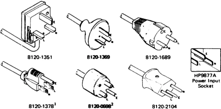
Power cords with different plugs are available for the external tape memory; the part number of each cord is shown below. Each plug has a ground connector. The cord packaged with each unit depends upon where it is to be delivered. If your unit has the wrong power cord for your area, please contact your local HP sales and service office.
8120-1l&9 8120·1689
~
~
HP9877APower Input Socket
..
L I
8120·1351
8120-13181 81~ 8120·2104
1 UL and CSA approved for use in the United States of ~ and Canada when set for either 100 or 120 Vac operation.
2 ULand CSA approved for use in the United Stales of AIBaica and Canada when set for either 220 or 240 Vac operat ion.
[image:9.615.93.456.440.619.2]POWE R REOUI REMENTS
The HP 9877 A has the following power requirements:
• Line Voltage: 100 Vac
+
5%, -10% 'I'120 Vac
+
5%, -lOCAl Switch Selectable220 Vac
+
5%, -10% 240 Vac+
5%, -10% • Line Frequency: 48 to66
Hertz• Power Consumption (maximum):
I
I
I
- - " - " - - - I
Standard Option 002 3 tape drives Option 004
G~OUNDING REQUIREMENTS
100/120 Volts 1.5A 1.7SA 1.8A 2.0A
220/240 Volts 700mA 800mA 860mA 920mA
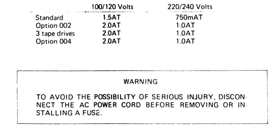
FUSES
The fuse irstalled in the external tape memory oepends upon the unit type and the power supply voltage. Check that the fuse installed in your unit conforms to the table below.
Standard Option 002 3 tape drives Option 004
100/120 Volts
----+---.---~
1.SAT 2.0AT 2.0AT 2.0AT
WARNING
220/240
Volts750mAT 1.0AT 1.0AT 1.0AT
TO AVOID THE POSSIBILITY OF SERIOUS INJURY,
DISCON-: NECT THE AC POWER CORD BEFORE REMOVING OR
IN-L
ST AL LI NG A._FU_S_c_. _ _ _ _ _ _The fuse is located on the rear panel of the external tape memory to the left of the power socket. To change the fuse, disconnect the power cord to the unit. Remove the fuse cap by pressing inward while twisting it counterclockwise. Remove the fuse from the cap and insert the correct replacement fuse (either end) into the cap. Put the fuse and cap back into the f'''';3e holder. Press on the cap and twist it clockwise until it locks in place.
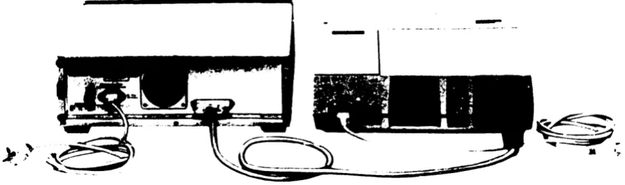
EXTERNAL TAPE MEMORY/CALCULATOR CONFIGURATION
Place the external tape memory and calculator on a flat surface where they are to be used. Raise the two front tilt stands located underneath the front of the HP 9877 A.
CAUTION
The interface connector must not be inserted or removed from the external tape memory or calculator with the power on. To do so wi II cause dam3ge tL the equipment.
[image:11.613.52.488.101.313.2]-\.. .. ~
I ) '
..
Figure 1-2. 9877 A/9825A Configurat ion
INITIAL TURN-ON INSTRUCTIONS
1. Set the external tape memory voltage selector switche!' to the setting applicable to your a.c. mains supply. The voltage selector switches are located on the rear of the unit. Switch settings for the nominal line voltages are shown below.
100 Volts 120 Volts 220 Volts 240 Volts
2. Check that the calculator voltage selector is set to the cn~rect position (see 9825A Cal-culator Operating and Programming Manual).
3.
Connect both the external tape memory and calculator power leads into a.c. mains sockets.4.
Using the switches on the front panel of the external tape memory, and on the right hand side of the calculator, switch on the power.EXTERNAL TAPE MEMORY CLEANING
Case
The external tape memory case can be cleaned by using a soft, moist cloth. Do not use harsh or abrasive detergents, and do not allow moisture to penetrate the external tape memory.
Fan Filter
[image:12.613.89.536.36.168.2]Magnetic Tape Head
To ensure the reliability of tape operation, it is recommended that the tape head be cleaned after every eight hours of tape operations. It's a good idea to clean the tape head before making important recordings.
The tape head is cleaned as follows:
1 . Remove the tape cartridge if installed.
2. Clean the tape head with a cotton swab that has been dampened with head cleanir.~
solution (HP part no.
8500-1251).
Wipe the top of the tape head a few times with the cotton swab. Remove any other dust that has accumulated in the vicinity of the tape head.CONDI TIONING THE TAPE
Repeated 0perations over a short length of tape (usually less than
4000
bytes or1.5
m (5 ft.)) can cause slack (extreme changes in temperature can also cause this). The outer layer of tape can slip and rub on the cartridge, causing damage to the tape. I f operation continues, the tape may jam and be ruined.NOTE
This problem is most likely to occur if exclusive use is made of one file or two adjacent files near the beginning or end of tape.
If a particular application requires such operation, this slack can be prevented by condition-ing the tape periodically. For example, for a tape with
80
files where only files0
and 1 are used, execute the following program segment after every200
operations on file0
or 1:B:
fdf:::~1TAPE CARTRIDGE CONSIDERATIONS
I f the tape unwi nds completely fror,l one of the reels, refer to Figure 1-3 and use the ~ro
cedure below to rethread the tape.
1. Remove the 4 screV'.s holding the cart-rirl~~ :C've-f tir'J(J ~umove the cover.
2. Thread the tape around the guides as shown in Figure 1-3, making sure it passes through the tape scraper.
3. With the tape extended almost to the drive belt, moisten the end of the tape so that it wi II st ick to the take-up reel.
4. Use a pencil (or other sharp instrument) to guide the tape between the drive belt and the take-up reel. Keeping the tape taut, wind the tape onto the take-up reel using the pencil.
5. As you wind the tape onto the reel, ensure that there is no slack in the tape. If the tape is not tight, repeat the operation. Be sure the tape follows hub around for the first turn.
6. Wind at least 20 turns of tape onto the rp.el by turning the drive roller. I f any rollers creep up away from the plate, press them back again.
7. Reassemble the cartridge.
tape scraper
[image:14.612.138.391.340.592.2]CHAPTER
2
SETTING UP PROCEDURES
GENERAL
The external tape memory cartridge units are Identical to the unit fitted in the calculator. Also, tape care, format ,,:\~u commands are ident ical. Therefore, before using the exterr.al tape memory the user should read :hapter 9 (tape cartridge operations) in the calculator operating and programming manual. The follewing chapter only provides the additional in· formation required to use the HP 9877 A.
SETTING THE SELECT CODE
The select code is a number by which the calculator identifies a peripheral device. When a select code is addressed in a prograrr t")r through the calculator keyboard, a communication link is set up between the calculator and peripheral. Although the external tape memory is
~ssentially one peripheral, each tape cartridge unit is considp"~d by the calculator to be art individual peripheral. The reason for this is that the, calculator can only service one tape cartridge unit at a time.
To provide the communication link between the 9825A calculator and a specific tape car-tridge unit in the 9877 A, there are two stages in setting up the select code. This is accom-plished by setting a switch on the imerface card and by a calculator keyboard entry or by specification in a peripheral control pr09ram.
[image:15.612.105.549.570.670.2]The select code number set on the imerface card (see Figure 2-1) identifies the HP 9877 A as a whole.
If
you also have other peripherals or instruments connected to the calculator each of these will be allocated their own code number. You must therefore choose a select code whose combination does not include a number already allocated to another device (see select code combinations). This number, once set, does not normally need to be altered again.The select code number entered througr 'lne Lliculdtor keyboard, or speclfred In a peripher~d
control proqrarl'l. Identifies the ,r,dl\lldual tape cartrldqe units. When the 9877A is being used as an external memory, the user muSt Identify the specific ctrtridqe eac:l time he wishes to use it by dddressing It In the control program or through the keyboard with the dppropriate select code. This includes the calculator built In unit which is always ident ifted by select
code number 1 (ssc ll.
When the unit is being used to duplicate a master tape, the DUPL ICATOR tape cartridge supplied with the HP 9877 A IS used. The program contained on this cartridge Includes the car
tridge select codes. Therefore the user only needs to set the tnterface card selector.
SELECT CODE COMBINATIONS
The select code numbers you choose to set on the 9877 A interface card and through the calcu-lator keyboard (or control program) are governed by various restrictions. It is important that you observe these restrictions in order that the 9825A/9877 A configuration functions cor-rectly.
Decribed below are the combinations of select codes applicable to each of the three versions of HP 9877 A.
NOTE
After upgrading it is possible to have a
3
tape drive unit. See Chap-ter3
for this special r.ase.L - . _ _ _ _ _ _ .
For all versions select codes 0 and 1 must never be used as these are allocated to functions within the 9825A calculator (0 selects keyboard and display and 1 selects the built-in car-tridge). I n addition, select codes 2 and
3
must not be used with option 004. I f either 2 or3
is used a mean ingless response will result. The select code combinations for each version is as follows:Standard (1 cartridge unit)
Option 002 ~2 cartridge unIt)
~
IT L
4
!
Ielect Code 2
3
1 5 6 7ape Cartridge ::1 ::2 :: 1 I ::2 ::1 ::2
I
8
1 9 10 ! 11 ::1: ::2 ::1 i ::21
II
12 I
I
,
#1 I
I
1~'
114:: ,) 1 ::
J.~1.5
1~
Select codes 2 to 15 inclusive are available. The code numbers are divided into pairs. To identify the 9877 A as a whole either number of a pair may be set on the interface card (e.g. 2 or 3; 4 or 5; 6 or 7 etc.). However, if either numbt::r of a pair is being used to identify another peripheral then neither number is available for use with the 9877 A. Also, whichever number you choose to St;t on the 9877 A interface means that its partner number cannot he used to identify other peripherals.
To identify the individual tape cartridge units, select codes must also be addressed through the calculator keyboard (or by control program). The select codes used here must relate directly to the number set on the interface card. For example, if 6 is set on the interface only 6 or 7 may be used to identify the individual cartridge units. For each number pair the lower number always identifies tape cartridge:: 1 and the higher number tape cartridge:: 2.
Option 004 (4 cartridge unit)
1
!
10r
Select Code 4 5 l
6
7
8 9 11 1213
141 15Tape Cartridge ::1
::2\
::3
::4 ::1 ::21 ::3
::4 :+1 ;:2#31
#4Only select codes 4 to 15 inclusive are available and these are divided into groups of four as shown above. To identify the 9877 A as a whole, any number of a group may be set on the interface card provided that this number, or any other number in it's group, is not being used to identify other peripherals. Similarly the number you choose to set on the interface, along with the other three numbers from its group, cannot be used to identify other peripher-als.
9877A SYSTEM TEST
This description contains 3 test procedure to verify the performance of the 9877 A. It is good
practice to initially check the 9825 Tape Cartridge, to verify that tr.e 9825 is working cor-rectly.
Then run the test as follows:
1. Turn on the calculator and external tape memory.
2.
Insert the System Test Cartridge into the tape cartridge unit to be tested.3.
Press:( \
8EJC~lU
o
0 0
xx0
(where xx=
select code number1
800m
4.
The calculator display will show:[
:~ ~T
_t_","_,i __
- _ _ _ _ _ _ _ _ _ _ _ _
__'
5. Press:8 (
eO.TO_I]
6.
The following display and printout should be seen:CARTRIDGE TEST
7.
Remove the System Test Cartridge and insert a scratch cartridge* , then press8.
8. After about 45 seconds the following display and printout should be seen.REPLACE TEST CARTRIDGE
9.
Remove the scratch cartridge.,',CARJRIOGE
TEST
~COM'PLETE
.
CHAPTER 3
FIELD INSTALLATION
FITTING THE FIELD INSTALLATION KIT
The following procedure describes the field installation of the 11242A field installation extension. You should read 'Assembly Access' (Chapter 5 of this manual) before any kit installation to get faiTtilidf with the 9877 A construction.
Proceed as follows:
• Remove the front panel assembly as described in 'Transport Assembly', Chapter
5.
• Remove the four screws from the left most panel f·iller (looking from front) in the sub-panel and the front sub-panel.
• I nstall the tape cartridge unit and the tape drive. • Replace the panel assembly.
• Remove the filler boards.
• Set the "Option" switches as described at the end of this Chapter.
• Connect the right most tape unit (looking from front) with the lowest transport logic board. Connect the board above with the next tape unit on the left and so on.
• I nstall the new transport logic board at the place of the lowest filler board and connect it to CARTRIDGE #
1.
• Upgrade the boards with filler boards if needed.
• Check and replace the fuse if necessary (see Chapter 1 for fuse ratings).
Three Tape Drive
UnitAfter upgrading, it is possible that a customer has a 9877 A unit with three installed tape car-tridges. As there is no description in the operating manual for you to cover this possibility, check the following points for a correctly working device.
• Set the "option" switches as described at the end of this Chapter.
• Use the select code-combinations as for option 004. The select code numbers 4,8 and 12 of the three possible corminations are not used in this case, you can use them in the same manner as code numbers 2 and 3 for other peripherals connected to the calculator.
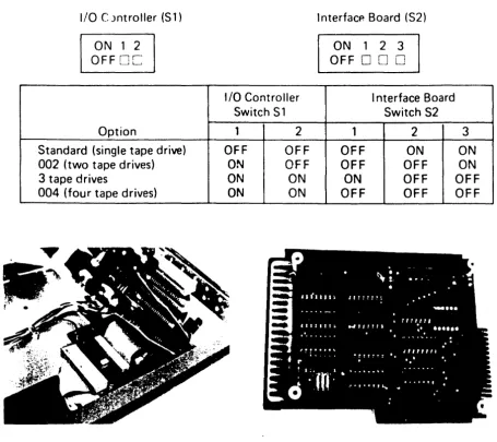
SETTiNG THE "OPTION" SWITCHES
Depending upon which option is installed in the External Tape Memory, the switches on the I/O Controller board and interface board must be positioned in the following way:
I/O C )ntroller (S1)
ON 1 2 OFF
0
c:
Option
Standard (single tape drive) 002 (two tape drives) 3 tape drives
004 (four tape drives)
1/0 Controller Switch S1
1 2
OFF OFF
ON OFF
ON ON
ON ON
Interfacp. Board (S2)
ON 1 2 3
OFF
0 0 0
I nterface Board Switch S2
1 2
OFF ON
OFF OFF
ON OFF
OFF OFF
3
ON ON OFF OFF
[image:20.617.48.504.88.493.2]CHAPTER
4
THEORY OF OPERATION
INTRODUCTION
This chapter provides the principles of operation of the external tape memory. It includes a block diagram, a general description and a brief theory of operation for those boards which are on component level repair. Schematic diagrams of the PCB's are given in Chapter 6,
Figures 6-4, 6-5 and 6-6.
LOGiC DEFINITIONS
The following logic conventions are used when describing the tape memory signals:
• Logic levels are nominally 0 volts and +5 volts;
OV
is referred to as the "Iow" state and +5V as the "high" state.• The mnemonics, which are given to the logic signals are of two types:
1. Those with a bar over the characters are true when they are in "low" state.
2. Signals without a bar over the characters are true when they are in "high" state.
BLOCK-DIAGRAMM (OPTION 1.1
EXT TAPE ~
CALC
r---~----~~.~
POWER POWER -'lt1V
-'2Y -12Y
- SY MODULE SUPPlY
ASSEMBLY ASSEM8l.Y
[image:21.613.126.502.416.672.2]46 - SY
GENERAL DESCRIPTION
Interface Card (A 1)
The
9877 AExternal Tape V1emJry functions with the
9825ACalculator using the dedicated
'nterface
09877 -07901 wh;r:~":;, delivered with the External Tape Memory.
The I/O card plugs into any of the calculator
liD
slots. The funct ion of the I/O card is to
provide the select code for the external tape memory and to co-ordinate and buffer the data
exchange between the calculator and the external tape memory. When the sending device has
data
1'0be transferred, the
1/0
card accepts the data, performs any necessary buffering and
logic operations, and outputs the data when the receiving device is ready. Power for the
1/0
card
isprovided by the +5V from the calculator.
Mnemonic list for the external tape memory
PA (0-3)
Peripheral Address
INIT
Ini!ialize
INT
lilterrupt
DOUT
Data
Out
IOS8
I nput-Ou-:put-Strobe
CTL
(1-2)Control Li.1e
DMAR
Direct Memo,'., Access Request
FLG
Flag
STS
Status
100
(0-7)
I nput -Output
0at a line
MYPA
MyPeripheral-Address
SHLD
Shield
1/0
Controller (A2)
•
Record ing System
The recording system consists of h-.O major assemblies.
• The tape transport logic board.
• The tape transport drive assenlbly.
These assemblies control the data transfer between the tape cartridge and the calculator.
Tape Transport Logic Board (AJ)
The tape transport logic board contains the following circuits.
• Control and timing
• Command latch
• Status registers
Tape Transport Drive Assembly (A4)
The tape transport drive assembly consists of an analog board and the motor-tach assembly. The analog board supplies (or receives) serial data to-or-from the read/record head and con-tains the servo motor control circuits. The motor-tach assembly drives the tape cartridge as required by the analog board.
Power Supply (AS, A6)
The power module assembly and the power supply assembly provides ±20V, !: 12V, and ±5V
to the external tape memory.
THEORY OF OPERATION
NOTE: The symbol. indicates the 'AND' function.
I nterface Card (A
1 )
U
1
(open collector outputs) compares the select code chosen by the select code switch on the Interface Card with the four per.pheral address lines PAO - PA3 during an operation. For each version of the 9877 A this operates as follows:- Standard (single cartridge) unit. MYPA. INT goes high when PA3, PA2, PA 1 and PAO agree with bits 3, 2, 1 and 0 of the select code, and the I NT iine is also high.
- 002 (two cartridge) unit. MYPA. INT goes high when PA3, PA2 and PA 1 agree with bits 3, 2 and 1 of the select code, and the INT line is also high.
U2 and U5 are used as line drivers and tri-state buffers. During data-exchange U2 and U5
are enabled with a low DI5AB signal. Only when the reset key is pressed, or when the
9877is
switched on, the DI5AB line goe! high for 1,4 j.Js and disables these buffers fcrcing the
output-lines high.
U3,U4 and
U9are tri-state buffers, which allow input or output transfer with
A2. With a low output at
U7pin
8,data can be transferred from the external tape memory
to the calculator. With the inverted signal at
U7pin 12, data transfer is enabled in the other
direction. The option s'wvitch 52 is used to select the addressed transport logic boards together
with
U 1 A, U 1 B, U 1 C and Ul D. It's position depends upon the option (see Chapter 3, setting
the "option" switches).
The external tape memory can
pulldown the
~and 5T5 lines when the calculator wants
the
9877to input or output data. These
twolines are enabled with a high MYPA •
INT
signal (which is inverted in U6 and enables the tri-state buffers
U 1
D).The DMAR line should only be enabled when in the search mode. Q of the D-Flip-Flop
Ul 1
enables this line. The condition for the clock pulse of
U11 is:
Clock
=
D OUT. IOSB. CTL
1 •INT. MYPA. CTL2
I/O Controller (A2)
The I/O Controller selects one of the transport logic boards. This is addressed by its
sel~ctcode via the interface-board. Every transport logic board has its internal select code. To
address each of the transport logic boards, two of these lines are required:
The lines PA 1 (transport logic boards 1 and 2),
PA 1 (boards 3 and 4),
PAD (boards 1 and 3) and
PAO (boards 2 and 4).
To address for example, board 3, PAO and PA 1 must be high, and PAD and PA 1 low.
Depending upon the option and the positions of the "option" switches (see Chapter 3),
there are up to 4 transport logic boards addressable via the interface-board. The resistors
R2, R3 and R4 are used to avoid line noise on the interface cable. U3B, CR1, 01 and the
resistors R5, R6, R7 and R2 are necessary for a correct INIT signal. The INIT line goes low
when the reset-key is pressed or when the 9825 is switched off.
The PVAL signel is derived from the 9877 A power supply and suppresses any command to
the transport logic boards during a powpr failure (PVAL - low).
U4.A. is triggered with a high going collector output at Q 1, and outputs a 1,4 J..Ls pulse, refer to the timing diagram below (Figure
d-2L
I~
I
O(U4P,) ~I
I
- - - . l.4pS - -
- 4-1
OIU4~~
______________ . ____________________________________~1
Q(U4~~
________~~~
__________~
,. O.75~S---.
1..--
O.3pS ~ I~O.3pS ~IL-..--_-....ll
, - - - I _ __O(U5B)
U
U
~.lIJS*- --+IO.lpS~
Q(U4~
State 1
[image:25.615.84.548.75.388.2]+
State 2+
Figure 4.2. Timing Diagram
Q
of U4A forces CTl2 low during this period. Q of U4A clocks U48, which outputs a 0,75~s pulse, and this holds the CTl 1 and DOUT lines low for the period of the first word.Q of U4A also triggers one-~ot USA. With the trailing edge of the O.~ulse at output Q of U5A, U5B is triggered and Q of USB goes low for 0.1 JlS, forcing the IOS8 line low.
With the low 10SB signal, state 1 is latched in the transport logic boards.
CTl1 CTl2 DOUT IOS8
State 1 0 0 0
0
State 2 1 0 1
0
With the trailing edge of Q (U4B), U5A is triggered again and U5A Q goes high for a second
Power Supply
The power supply provides six different voltages and one status signal to the calculator. The voltage lines are used by the various circuits, as shown in Figure 4-3 for power distribution. PVAL is used to suppress any command to the transport logic boards when going low (power failu re).
+ 20 -·20 +12
+20 -12 -20
POWER +12
SUPPLY -12
+ 5
.s
-5 -5 [image:26.615.98.394.117.266.2]PVAL.
Figure 4-3. Power Supply Block Diagram
+5 Volt Supply
The +5V power supply utilises a switching regulator technique to provide maximum output current with minimum heat dissipation by the series pass transistor. Since
03
draws current only when saturated, power dissipation in 03 is minimised.02 is switched by a small voltage difference between U4 pin 2 and U4 pin 3 (inputs to the IC operational amplifier). A +5V reference is established on the amplifier non-inverting input (pin 3) by voltage divider R 14 and R 16. When the supply output is less than the reference Voltage, U4 switches 03 on. The +20V 03 collector voltage, divided by R15 and R17, estab-lishes a higher reference voltage. When the supply output increases to the higher reference Voltage, U4 sWitches 03 off and the previous reference decreases to the level originally estab-lished by R 14 and R 16. 03 is switched on when the voltage output is again equal to the ref-erence voltage.
The 03 output is a 20V square wave, which is filtered by L2 and C10. The output of the filter (+5V) is the average of the 03 collector signal. C R5 provides a continuous path for inductor (L2) current when 03 is off. L 1 isolates the capacitance of Cl 0 from external filter capacitance, couples the ripple voltage to the +5V sense line and provides additional +5V fil-tering.
CAUTION
--5 Volt Supply
The source for the
--5
Vf)it supply '5 !t1.e -12 volt supply. C R8 and R7 establish the 5volt supp;y. An addition<tI resistor. R 1 (82 ~2), is soldered to the edge connector between pins Lend 17. This provid~s a higher current output at the -5V power supply.
+20 Volt and - 20 Volt Supplies
The -+20 volt and --20 volt supplies are unregulated and filtered only by C1 , C: and C \ _ These
voltages are used by the tape transport. They are also tl .~ source of power for the regulated
supplies.
+12 Volt Supply
The U3 internal reference zener diode provides a + 7 .15V reference for the operational ampli-fier ~. U3). The + 12V supply functions as a non-inverting amplifier wh ich amplifies the zener ieference voltage. The gain of the arT'plifier is determined by the voitage at the wiper-arm of the output voltage adjust, R 11. The range of this adjustment on the output voltage is typ-ically ± 0.5 volts of nominal.
R 13 (in conjunction with U3) provides current limiting for Q4.
The + 12V supply provides the reference voltage for the +5 volt supply, any changes or adjust-ments of the + 12 volt supply will affect the +5 volt supply.
-12 Volt Supply
CHAPTER 5
TROUBLESHOOTING
INTRODUCTION
This chapter provides assembly aa:255 and troubleshooting procedures. 1.1 conjunction with the theory of operation and the sdIIematic diagrams (see Chapter 6, Figures 6-4, 6-5 and 6-6) it wi II aid you in the repair of the 9877 A External Tape Memory.
ASSEMBLY ACCESS
Disconnect the AC-pcMer cord, before removing any external tape memory assemblv_
Most of the 9877 A assemblies
mar
be accessed by removing the screw located on the back of the top cover. Then slide thebJpcover backwards and remove it. [image:28.612.196.481.426.691.2]cover relec!Se SCIlWS
Transport Logic Board
To remove the transport logic board, press the removal tool (paper spindle from calculator) down over the white keepers, one at a time, while lifting that area of the PC board. To remove the board from the stack, remove the cable connectors, pivot the board and then disengage the hinge, by sliding it forward (about 1 cm).
The other transport logic boards are accessed in a simi lar manner. To remove the board, which is conner-ted to the left most tape unit, remove the two screws at the handle on the left side of the case and slide the left side panel backwards.
Power Supply Board
To remove the power supply, remove the three screws from the heatsink shown in Figure 5-1 and remove the heatsink. The power supply board can now be lifted out of its edge connector and removed. Do not remove the heats;"k from the power-supply board, if the 9877 A is to be turned on.
I /0 Controller
With the transport logic boards removed, the
liD
Controller can also be removed. To do so, remove the screws at the corners of the board, remove the cable connector to the back panel and the +5V and PVAL single pin connectors.Power Module
To remove the power module, remove the right side of the case and release the two screws which secure the power module to the case. Release the four corner screws in the base of the power module (note, one of these screws hds a ground lug). Remove the screw holding the power cable to the power module
case.
Unsolder the wi res to the voltage selector switches. Lift the power module from the chassis.Transport Assembly
To remove the transport assembly,
1. Remove the top Gover and the bottom cover of the 9877 A. To do this, remove the two screws shown in F igu re 5-1.
2. Disconnect the installed tape units and transport logic boards. To remove the plug from the left most tape unit it is
necessary
to remove the left side of the unit. This is possible when the tNO screws by the left handle are removed. Then slide the left side panel back-wards and remove it.3. Disconnect the power switch and the LED.
5. Remove the top trim as shown in Figure 5·2 and the side trim from the left and right side to gain ac.cess to the tape unit securing screws.
6. Remove the screws on the left and right side (two on each side) and on the top and bot· tom cover (thref! on each).
7. Slide all the tape units, together with the front panel, forward.
[image:30.613.133.480.174.692.2]8. To remove a tape unit, rem::>ve the four screws and remove the unit, see Figure 5-3.
TROUBLESHOOTING
INTERFACE CARD (Al)
The following procedure assumes, that the problem has been isolated to the A 1 assembly.
Visually inspect the bOi3rd for ddmaged cc,mponents or foreign conductive materials. I f any defects are found, they shou Id be corrected before proceed ing fu rther.
• I f the external tape memory fails to work completely. check the address circu its U 1, U2 A - C, U6A, U6B, USB and the flag and status lines U9B. U9C.
• If the 982S does not read or write data correctly or if the calculator does not accept 9877 A status, check U4, U3, UB, U7A, U7B .. USE.
• If calculator commands are not accepted correctly, check the tri-state line drivers U2
D -
F,US
D - F.
• If the 9877 does not work correctly in search mode, check U9A, Ul0, U7C, U6
D -
F,'!' If the drives are not correctly addressed, check the position of the select code switches.
Also check U1A, U1B, U1C and U1D and replace if defective.
'/0
CONTROLLER (A2)The following procedure assumes that the problem has been isolated to the A2 assembly:
• If the 9877 A dOEsn't stop working when the reset key is pressed, or when the 982S is switched off, check U 1 ,. C R 1 and 01 and replace if defect ive.
• If the 9877 A does not start working check if 01 collector is high. If not, check U 1, CR 1 and 01 and replace if defective.
• If 01 collector is high, check disabla line at U4A pin 13, it must be low for a correct work-ing device. If not replace U4.
• Check U60, U6A, U6B, U6C and replace if defective.
• If with the first cassette operation Error 43 occurs in the calculator display, check U4 and U5 for correct output pulses (refer to the timing diagram, Figure 4-2) and rep~ace if defec-tive.
• If more than one cassette starts working at the same time, check U2B and U2C and replace if defective.
POWER SUPPL V ADJUSTMENTS AND CHECKS
+12 and +5
VoltSupplies
The reference vc.ltaqe fo:- the +5 Volt supply is provided by the + 12 Volt supply, adjustments will affect the +5 V~lt supply. Each of these voltages should be checked and rechecked after making an adjustment to the +12 Volt supply.·
Other Suppl ies
Th~ remaining supplies are non-adjustable but their output can be checked for proper opera· tion. Refer to Table 5-1 and Figure
64
in Chapter 6 .
.--Nominal Tolerance L~wer Limit Upper Limit
Voltage (Absolute value) (Absolute value)
Adjustable
+12 ~2% +11.76 +12.24
(R 1 1)
+5 ~3% +4.85 +5.15
Non-Adjustable -5 ±5% -4.75 -5.25
!
-12
±5% !-11.4 -12.6
[image:32.613.89.533.167.636.2]I
Table 5-1. Power Supply Voltage
-20V
+20V-5V Figure 5-4 Power Supply Test Points.
POWER SUPPLY CHECKS
[image:32.613.95.523.171.337.2]Check the supplies in the ~ollowing
sequence-! 20V Power Supplies
Before checking any of the other voltages, check the output of the full-wave bridge rectifier for !20V (unregulated). If this output is satisfactory, check the other supplies.
- 12V Power Su pply
I f the - 12V power supply is defect ive, change U2.
- 5V Power Supply
I f the - 12V power supply output is satisfactory, but the - 5 V output is incorrect, check C R8. Replace C R8 if it is suspect. If the current output is insufficient, check resistor R 1
(82 n) at the edge connector.
+ 12V Power Supply
To troubleshoot the
+
12V power supply,• I f the power supply is not within the specifications, adjust trim-pot R 11 to obtain the correct power supply output.
• Check, and replace if defective, fuse-resistor R 13 and 04.
• Replace voltage-regulator U3. Then adjust pot R 11 for the required power supply output.
+5V Power Supply
As the +12V power supply provides the reference voltage for the +5V regulator U4, any changes in the + 12V output will affect the +SV supply.
• Check 03. The collector output of 03 must be a 20V square wave.
• Check CRS, replace if defective.
• I f the collector output of 03 is still not switching, change U4.
• Check 06, replace if defective.
• Check
as
and C R7, replace if defective.• Check L3, L2 and C10 and replace if necessary.
Power·Valid Circuit (PVAL)
• I f the +20V and +SV supplies are within range, but the PV AL level is not within specifica-tions (+5V), check CRS, replace if defective.
Repeor ,he 110_
IUPOIva.v·,
M.A6
No
No
'.
0-00 .... _ " " , , , . "0 Con II 01'" A'J.
'I:> _ _ .,..., • • oft ,,,. C(JI,et;1 pe .. ',on ' - !9 .. - - . ... '.CkK-hon t~,." .nt1 'un
~_ . . . _ ' ' ' ' ' ' ' . ' ' no, c.o"tt<tlld
--
....
-9.
[image:34.617.50.545.22.719.2]o.o.p _ f,.neporl LottC
... ~'o,,,.,.~
_ - " II no, work.", . . . . " . ,
o.a tar __ •• or and
. . . conNCtlOM
____ .... bcwdt..
o.a ... iIur . . . . ", _ - - . ' . . . 0
-... _ _ 'O_"Y' .... ' , ..
"'._Iting
correctlyC'-k ,,,. wlK1 code _let-to ... ,he' ., ., .., fcor
,,.. wlK1 code bel"'''''': If 10. chene- , ... In, .. teu
c...dAI.''''' ....
c._
1f.', ... ,epe,,' ... AI . . v. rtno'. c.o", . . . ,,, , , , . , , . .
DttmnnK1,he
f t . _ t LottC
80erdt AJ. checll
~",pptv
...
'"No
CHAPTER 6
REPLACEABLE PARTS LIST
Table 6-' Replaceable Parts List
REFERENCE
-hp-DESCRIPTION
DESIGNATOR PART NO.
Al 09877-66501 SO A Y Interface
Cl 0160-0174 C: 0.47 MF 25V
C2,C3 0160-2055 C: 0.01 MV 100V
Rl 1810-0076 R-Network 1,8K
R2 1810-0125 R-Network 8 PIN
R3 1810-0142 R-Network 470
n
R4,R8,R9 0757-0283 R2K 1%0.125W
R10,R11,R12 0757-0280 R1K1%0.125W
R13 0757-0437 R 4,75K 1%
U1 1820-1297 IC 74 LS 266 N
U2,U5
1820-1491 IC SN 7407
U3, U4, U8, U10 ICSN 74 LS 367 N
U6 1820-0471 IC SN 7406
U7 1820-12G2 IC SN 74 LS 10
U9 1820-1201 IC SN 74 LS 03
U11 1820-1112 IC SN 74 L5 74
52 3101-2096 Switch
A2 09877-66502 SO AY liD Contr.
C1 0160-0174 C: 0,47 MF 25V
C2, C3, C4, C5 0140-0193 C: 82 PF 300V
- 0360-1705 Connecto r 40 PIN
R1 0757-0437 R 4,75K 1%
R2 1820-0142 R-Network 470
n
R3 1820-0076 R -Netwo rk 1,8 K
R4 1820-0125 R-Network
R5 0757-0410 R: 301
n
R6, R7 0757-0430 R: 2,21 K
R9 0757-0427 R: 1,5 K
Rl0 0698-3359 R: 12,7 K
Rll 0698-3258 R: 5,36 K
R12 0698-0084 R: 2,15 K
R14 0698-3159 R: 26,1 K
U2 1820-1255 IC: OM 8098
U3 1820-1197 IC: 74 L5 00
U4,U5 1820-0579 IC: 74123N
U6 1820-0668 IC: 7407
Ql 1854-0071 TR NPN
CRl 1901-0040 51-DID
51 3101-2061 Switch
[image:35.612.103.561.161.684.2]Table 6-1 Replaceable Parts List (cont.)
REFERENCE
-hp-DESCRIPTION
DESIGNA10R PART NO.
AS 09825--66551 Power Supply Assembly
Cl, C2 0180--2405 C: Fxd 6400 pf 25V
C3 0180--0408 C: Fxd 5400 pf 25V
C4 0180--0229 C: Fxd 33 pf 10V
CS,C6,C12 0180-0210 C: Fxd 3.3pf 15V
C7
o
180--'{) 1 06 C: Fxd 60 pf 6VC8 0180-2614 C: Fxd 100 pf 30V
C9 0180-1701 C: Fxd 6.8 pf 6V
Cl0 0180-2208 C: Fxd 200 pf 10V
Cll 0150-0071 C: Fxd 63 pf 15V
C14,C15 0180-1714 C: Fxd 300 JJf 15V
CRl thruCR4 1901-0662 010: Power Rect.
CRS 1901~11 010: 51 IN 3889R
CR6 1902-3190 010: ZNR 13V
CR7 1901-0040 010: 51 .05A 30V
CR8 1902-0533 010: ZNR 4.00V
Ll,L3 9100-3462 Inductor
L2 9100-3488 Choke
01 1854-0094 XSTR: 2N3646
02,05 1845-0071 XSTR: 2N4398
04 1854-0063 XSTR: 2N3055
06 1853-0045 XSTR: 2N4036
Rl,R2 0683-4725 R: Fxd 4.7KM 5%
R3, 0683-3325 R: Fxd 3.3KM 5%
R4, R18 0683-1025 R: Fxd 1Kn 5%
R5 0757-0410 R: Fxd 301 n 5%
R6 0757-0399
R:
Fxd 81.5 n 5%R7 0686-1815 R: Fxd 108 n 5%
R8 0812-0037 R: Fxd 5n 5W
R9 0698-4431 R: Fxd 3050 n 1%
Rl0 0698-3151 R: Fxd 2870 n 1%
Rl1 2100-2061 R: Var 200 n 10%
R12 0757-0274 R: Fxd 1210 n 1%
R13 0811-3414 R: Fxd 0.2 n
R14 0698-4461 R: Fxd 698 n 1%
R15 0698-3557 R: Fxd 806 n 1%
R16 0757-0416 R: Fxd 511
n
1%R17 0757-0270 R: Fxd 249 K 1%
R19 0683-1005 R: Fxd 10
n
5%R20 0683-2205 R: Fxd 22
n
5%R21 0683-2215 R: Fxd 230 n 5%
R22 0811-3069 R: Fxd 1
n
R23, R24 0683-1045 R: Fxd lOOK
n
5%Ul 1820-0430 IC: LM300K
U2 1826-0123 IC: LM320K - 12
09825-01101 Heat Sink - Fxd
09852-01102 Heat Sink - Removable
09825-64101 Insulator - 03
0340-0155 Insulator - 04, U1, U2
[image:36.620.63.482.72.716.2]Table 6-1 Replaceable Parts List (cont.)
REFERENCE
-hp-DESCRIPTION
DESIGNATOR PART NO.
1 09877-00101 Chassis
2 9100-3455 XFMR
3 09877-66502 liD-Controller Assy
4 3160-0209 Fan
5 09877-00202 Panel- Rear
6 09825-66561 Transport Logic Board
7 09825-66551 Power Supply Assy
8 09877-00603 Power Supply Shield
9 09877-04701 Connector SP RT
10 09877-02301 Holder Transport Assy
11 09877-00214 Panel Filler
12 09815-67902 Transport Assy
13 5040-7827 Cartridge Eject Bar
14 09877-00203 Sub-panel
15 09877-00211 Panel - Front
16 5040-8162 Rocker Switch
3101-2080
17 5082-4955 LED
18 09877-40002 Snap In
19 5040-7779 Door
20 2110-0467 Nut - Hex.
21 5040-7787 PC Hinge Half
22 5040-7721 PC Hinge
23 09877-01201 Fact Folder
24 1251-2500 Connector PC 12 Contacts
25 1251-0334 Connector PC 36 Contacts
26 2110-0470 Fuse Holder - Hex
2110-0465 Cap Fuse
27 11201-24701 Support-Fan
28 5040-8248 Fan-Filler
29 09877-61602 I nput Cable Assy
30 3150-0233 Filter - Foam
09877-67902 Cable Assy - Rear
31 1251-0086 Connector 50 m Plug
32 5040-7860 Cable - moulded
33 98032-66502 Configuration Assy
34 5040-8173 Cover - Right
35 5040-8174 Cover - Left
09877-67901 Interface 8 Bit (Complete)
36 09877 -66501 Interface Assy
37 5040-8161 Case - Left
38 5040-8158 Spring Latch
39 5040-8153 Case - Right
40 0380-0632 Spacer Snap-in
41 1251-2357 Power Connector AC
42 3101-2042 Switch - SI ide
43 0403-0150 Guide
44 09877-02303 Holder XFMR
45 09877-02304 Holder PC Board Front
46 09877-02305 Holder PC Board Rear
[image:37.613.106.537.73.708.2]The following parts also have an excharlge JB1~mber as they are in the blue stripe exchange program.
REFERENCE -hp-EXCHAMiE
DESCRIPTION
DESIGNATOR PARTfiO.
6 C9825-69561 Transport Logic Board
12 0981!HmJ2 Transport Assy
REFERENCE
-lip-DESCRIPTION
DESIGNATOR PART NO.
60 09877-04113 Cover - Bottom 61 09877-04112 Cover - Top 62 5020-8803 Frame - F rant 63 502O-BM Frame - Rear
64 ~ Strut - Corner
65 098n-04111 Cover - Side
66 5OO1~ Gusset - Side
67 5040-7201 Foot 68 5001-001 Trim - Side
69 5()6(HIIJ3 Strap - Handle
70 5040-7201 Cap - Rear
COMPONENT SIDE A5~1
""~"!Ir,r;'ft",,.~-,'~
C2
a: o
~
-'
: )
u
-'
~
u o
...
COMPONENT SIDE A1
HP Part NO 09877-66501
[image:39.1224.130.640.210.425.2]COMPONENTSIDE A2
@
[image:41.1224.210.1144.66.697.2](Sub-assembl ies)
~-t20~
I81
I
-- 2<ll - -~
--120--- --~
r
pOWER ·SUPPLY ASSEMBLY CAl'''''·m''
~~J---),-J~
>--
~--~~--~---~---.---L_
AIS 806 CR6 1)\1 C,) ~)) Al RI7 2L9K 33K An 1001< A7 180~ ____ ~ ______________________ ~~·~ __
~)17>--CR8 C 6 L9911 ~ll
\7
\JAI
, 7K
02
A2
, 7K
01 .I2V
PIIAL
1])--+
C7
I
~60
D'~~ _ _ R~121~(~FU~~~R~E~S~IS~TO~R~J _ _ ~ ______________________________________________________ ~---~.~12~V~--~,,>-T
·
~~
i~
·7.I5V ... -r.= ...
---..J
'tl2 2'10
10
~~---~--~--~---~.,~~~S~EN~~~--~U>__
R2' R9 lOOK 1270
RII 200 RIO
1910
R8
S UI
[image:42.1224.256.1155.53.714.2]Al INTERFACE BOARD 09877-{i651)1
TO CALCULATOR
o
1, - 1 B 2 ~ I' ~ I'
I'
AUT
R P S T 10 ~ I, r--_ _14+-_ _ _ 5+-_ _ ,6-+-_________ B
::.:6't.:!/S1T 0
I
~
r-_--+ __
-+ ___________
8!:!!?-t<D81T ,11
~ ~
r - r - } I I~
" -ft(
=t
2
82~81T
2 : SELECT
2 I ! > : ' 1 14 12 I . - - ~~ 1 28/ \U2A 81~,
?
COO£ SWITCHI
'1-K~+~:
:
~
':
'l.-f-?+~'
" ,,''':, ."
.:,
~o
U5:
5~:/-/,,,,,,,,
- - t - - - t - - - 'J
" f l I T ) !I
I
13 11 5I
f7~
1 , ! : ; 1) 11l
~
C) 5 I - - J 1 - - . 1 8::' 5VI
~~"
"..c-I
~
• ..
oJ''~. ~
, II''"'
,<-,",,0-I
h~~~~il~~~~
~~~8~~~~-'"~~~U:~9~ '~K~m ~~ ~~ ~~
I
I
Ll
~~
Ll
L
r;'
~ ~
~
l
~l ~
" , 3
...---+--+--+--+--+-+-+--+-'-i' r -ro:::t:~5~'~r-J~~-!R4~_O"5V
I~
¢
Q
I
' I
"
~
I
\"'~~
_
_<~X· ~~
I l L109 '~ "J ...--_--="<x" _UIiO~9:...-+_-+_--+--+_-+_+_+--+__1? ~'_
12 I_
I
II~~rI3~--+-_+--+-_~-+-+-+--+-~2
I
..LA7R~'
~
) R3 fL-o"SV ~--~m~_KU6E~"~+--+--+--+--+-+-+---+-~:
I
..LAI " 6A 1 n U98
I
6t---; _ _ '0=3 12
I
I
~I
i
~RO
...L. ...--~-+--_ _r---~~ __ -~-_~--~~--+---+~ar- ~:~~1~----4--+--4--4-+-+-4--+-1~
9
) r - 6 1
~ Q,I-=---I
L -_ _ _ _ _ -+ __ -+ _________ ...,2
0 Ul1 ~10
2
r-12 7
Is
,
I
L1.
. r
R2~ li.. 176 ~.SV
) AI
5
~
Rt
.-_ _ +-... A~Il--() • !IV
.J..
Rn ~. Sv • 5Vo---... AIO
~ 1
"--
-I~
I~
I~
I~
TO EXTERNAL TAPE MEMORY VIA 1/0 CONTROllER
CON 2
[image:43.1229.63.1110.178.650.2]A2 I/O CONTROLLER,09877-&i502
•
I..
•
:>i-,r---I
II
r!-I
I. , 1
I
I
!i
27 I
.- I I
~
,18 'A /I 13 2!1 )1 29l
I 3 5 79
"
1) 15 ,I
,
12
"t~'"
51 !() U26 9 f-o H ~V
• !IV
-Sv
0 (
~
RIO R14
f
T
C2[=-"
1;13
1& 1514 10 r" 17 1&CL
I
B CLU4.o U4B 9
cr , a l!1..-- 1S 12
°ls
~
~
J~
U6B
,
Ii1
-5V
?
Rl
2 1 ] 4 15 iii 7 I
3 2 4· 5 Is 7
•
A4
I
RI
J!.
--'NIT
"
'0- 5V
?9
R2
I
] I' 1
6 Pi
.,
-!IV
,r.:-}
1.. <f
Rli~:: u38
- !IV 9
-Sv - 5V
:>
~
R9 R12 R5
Rl1
3
IT
esl:C
-SV PV.ol 12clT2 T3 16 115 h"- n
B CL
f~
"
I
I
~ USA
.~
• "I"
USB
FRO'" INTERFACE BOARD Al
FlG ST~ O"'AR GND GNO GNO " " ' J
"
"
" 17 19 ) ) )5 37 )9I
)() To a'i Transport logIC Boords To all Tronsporl loeJlC Boards
" 17
19 " 21
)~
I
Pili To TfU'\SPOl1 lDglC Iloc>n:a 14
Pill To Trunsport U>gc ~ 2.4
To 0'1 Transporl L"9IC Boords
) 2 1~ To Transport L<>iI'C Booms ,. )
" I 9"" I To Transport L"9'c
Boards 1 2
" 1
~
" 2
" 3
~ ~3
" --" 3
To all Transport LogiC
Board'S
2
2:) To all
Tron~r'
logiC12 Boards
34
, 1
-,
~ " , " 1 1) 15To 011 Tronaport Logic
[image:44.1224.247.1108.93.724.2]