AUTOMATIC "3-D" PLOTTING WITH THE TR-48
®
/DES-30 DESK-TOPANALOG/HYBRID COMPUTING SYSTEM by
Omri Serlin
INTRODUCTION
This study describes the development of a hybrid program for obtaining "3-dimensional" surfaces of temperature as a function of time and distance in an air-cooled glass slab. The purpose of the program is to demonstrate an effecti ve use of the TR-48/DES-30 Desk-Top Analog/Hybrid Computing System as applied to the simu-lation of a system described by a partial differential equation and towards the improvement of the. man-machine interface by providing a visual, "3-dimensional" display.
The logic for arranging the solutions from the TR-48 General Purpose Analog Computer in "3-D" format, and for controlling the plotting process automatically is supplied by the DES-30 Digital ExpanSion System. This general-purpose, low-cost digital logic package, especially designed for operation with desk-top analog computers, also provides mode control and other logic tasks as required in the high speed repetitive operation (rep op) solution of the system equations.
The DES-30 System, although capable of operating autonomously for use in digital design or instruction, was designed primarily as an expansion to the TR-48 analog computer to provide basic hybrid capabilities to the small computer facility. It also can be combined readily with other general-purpose digital computers to provide extended control functions. Thus, it makes available to the analog computer in this application, the necessary digital logic functions to implement this essentially hybrid program.
TABLE OF CONTENTS
Introduction . . • . . . • . . • . . . • . . . 1
System Description . . . . . . . . • . . . 3
Method of Solution . . . 3
Scaling. . . • . . • . . . • . • . . • . . . • .. 6
How the Program Works. • . . . • . .. 8
Analog Program . . • . • • . . . . • . • . . • . • . . . 9
Master Timer . . . . • • • . . . • . . • . • . . • . . .. 9
y-AxiS Switching . . . • . . . • . • • . . • • . •. 10
Fast-to-Slow Converter . • . • . . • . • • • • . . . • 10
3 - D Plot Control . . • . . . . • . . . • . . • . . .. 11
Appendix I: Boundary Equations . . . • . . . • •. 13
Appendix il: Static Test . • • . • . . . . • . . . • . . . .. 14
Appendix ill: A Typical Result
Appendix IV: Detailed Program
19
SYSTEM DESCRIPTION
The physical system of interest is shown in Figure 1. The problem is to investigate the cooling (by air) of a slab of glass (subsequent to heat treatment).
AU," AT "T" . ,
Figure 1: Glass Slab Being Air Cooled
In particular, it is necessary to determine how cold
the ambient air can be (how low T A can be) before severe temperature gradients in both space (x) and time (t) are developed. (Extreme gradients result in stress cracks). For this, it will be desirable to observe a "surface" of temperature T as a func-tion of distance x and time t.
Cooling is described by the one-dimensional heat diffusion equation:
where
T
=
f(t,x)k
01. =
-pc
METHOD OF SOLUTION
c
=
specific heatp
=
densityk
=
conductivity(1)
Normalizing the Variables: Equation (1) can be
sim-plified by using dimensionless variables as follows:
z
=~L
This results in
aT _
01.aT
at -
L2 09(normalized distance)
(2)
(normalized time)
(3)
and equation (1) reduces to
aT
(4)
09
Obtaining nO) and T(z): PDE(4) is solved in two
dif-ferent ways simultaneously: first, it is solved by finite differencing the z dimension (corresponding to distance) ; there results a set of basiC ally identical equations (see Appendix Ifor derivation of the equa-tions at the air-glass interface):
dT. T. 1 - 2T. + T. 1
---1
=
J+ 2 J J - (j=
0,1,2,3)d9 (boz)
(5)
where J IS the number of a given point in z.
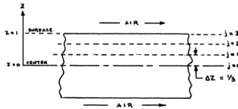
Refer to Figure 2.
II
-- AI,,_
'I.-I -~!!'~ - . . . - - - . - - - - -1" 3
-- ---1-:r.
*----j.,
'1_.
&'I.n • •- - AI1\
-Figure 2: Definition of Points for Space Finite Differencing
Second, it is solved by finite differencing the 8
dimension (corresponding to time) to get the set of equations:
d2T Ti - Ti _1
-2-i
=
A9 (1=
1,2,3,4)*dz ~
(6)
where i is a given instant in time.
The solution of equations (5) ("parallel" solution)
are T j (8) which describe temperatures as a function
of time for a set of discrete points in distance (the index j identifies the point).
Equations (6) ("pseudo serial" solution) yield Ti (z) which describe temperature as a function of distance for a set of discrete points in time (the index i identifies the point). Note that, for this solution, computer time plays the role of dis-tance, z. While all Ti(z) are produced simultan-eously with respect to computer time, they really
°i starts with 1 rather than 0 since at time 8 =·0 (t = 0) the slab is at
[image:3.617.57.293.122.218.2] [image:3.617.315.549.304.412.2]represent "sn!tpshots" of temperature distribution in the slab at progressively -later points in real time.
A Simplified implementation of one equation each of sets (5) and (6) is shown in Figure 3.
MO"'''
..
I
I
I I
+
"'."Ii.
ON • • L.~K O'
,,"&
PARALI. ... urr'.~-~L-I ~.aE
~----'--~~
I
Y
MO .. e
Figure 3: Typical (Simplified) Analog Blocks
Note from the computer diagram that the serial
solution is basically unstable. If it runs too long
(exceed the distance z = 1), it will surely blow
up (diverge). It will also tend to magnify noise.
This is one of the major reasons thepseudo-serial solution is rarely used.
Initial Conaitions: Another reason for not using the
pseudo-serial solution, is that the I.C.'s required
for it are usually difficult to come by. In this case,
the I.C.'s are:
T. (z
=
0) 1dTi
- (z = 0)
dz
for all i (all time)
for all i (all time)
Because of the symmetry of the system, it can be
said that:
dTi
(z = 0) = 0
dZ
(since, at the center of the slab..,-which is the center of symmetry -- the rate of change of temperature with respect to distance is zero). But Ti(z =0) is the temperature atz=O (center of slab) at time to, tl, ---ti, ---tn (where n = 4, in this case).
We can obtain these I.Co's from the parallel solution by having track/stores pick up the values To (0) at the instant ti and de~
liver these values to the I.C. inputs of the second integrator
[Ti(z)] in each block of the serial solution. See Figure 4
below.
-+--+-+--th' •
....
.• ..J
L
"T I "'IN II
Figure 4: Program to Obtain I.C. for the Semi Serial Solution
The DES-30 System generates the proper TRACK-HOLD signals for these track/stores during each operate (OP) period. At four equally spaced in-stances during the OP period, a monostable timer (MT) is set for about 100 fJ.S (the time necessary to assure proper tracking). Each time this happens, a 4-bit ring shift register advances one pOSition. The position of the circulating bit in the register is used to sequence the MT signal to the four track/ stores.
The I.C.'s for the parallel solution are Tj (8=0), the temperature distribution in the slab at time
() =0, which is known.
OP.IC Timing Control: To display the Tj«(}), Ti(z)
functions on the TR-48 scope, both solutions are run in RO controlled by a "master timer program" on
the DES-30. This program (Figure 5) generates a
[image:4.613.81.265.148.419.2] [image:4.613.320.553.182.403.2]I KC
1Io&"1f"
'TRAIN
,0 ,/s C.O"-'"TIllrOI..
,.tifOIi"'''JoI
Figure 5: Master Timer Program
aP
Ie
During the first run, because both solutions are operating simultaneously, the track/store units have not yet established the correct outputs and the I.C.'s of the pseudo-serial solution are incorrect. This situation is corrected on the second run.
Fast-to-Slow Converter (FSC): Solutions generated in
the RO mode t can be plotted on conventional x-y
plotters by means of a "fast-to-slow converter"
program. This program consists of two track/
store units cascaded as shown in Figure 6a. (Tim-ing for this program is shown in Figure 6b.)
To PLOTTCII Y A'II.'.
Figure 6a. Program for Fast-to-Slow Conversion (FSC)
'--_---'I
M~~,--________ ~nL
________
~Il~_ _ _ _
~r-LFigure 6b. Timing for Fast-to-Slow Conversion
The control signal, a, for the' 'Fast-to-Slow
Con-verter" could be generated with two integrators and an electronic comparator. To conserve integrators,
however, as well as to demonstrate DES-3~
capabil-ities, the control signal is generated by an all-digital program. This program operates as a vari-able on -time mono stvari-able timer, generating increas-ingly longer pulses in equal increments. These
increments can be made so small (47 J.l.S in this
program) that the output of the FSC can be plotted directly without smoothing.
With this control signal applied, TIS 34 "mem-orizes" the value of the highspeed solution at times T, 2T, 3T, . . . nT, where T is the basic increment (47 J.l.s).
T/S 35 accepts the high speed solution at T, then 2T, 3T, etc.; its output, therefore, is the value of the function at these instances, changing progres-sively at each RO run. Thus, after the first RO run, the output of T/S 35 is the value of the solution at t = T; after the second RO run, at t = 2T; etc. If the
tNo distinction is made between DES·3D.controlled OP-/C cycle and TR-48 RO-timer.controlled OP./C cycle; both situations are referred to as uRO u in this paper.
increments, T, are small enough, the output of T /S 35 will change only slightly between each
operate cycle. With T = 47 J.l.S and the OP time
being 12 ms, 256 runs are required for T/S 35 to "go through" the entire solution. Since 256 RO runs require 6.16 seconds, we obtain a function slow enough for plotting.
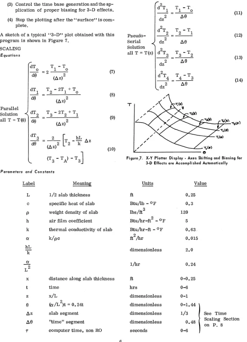
"3·0" Plotting: The focus of the demonstration is
the automatic plotting of a "surface" of tempera-ture, T, as a function of both distance, z, and time,
8, under DES-3~ logic control. The "3-D" effects
are achieved as follows: The function To(O) is
plotted with a constant negative bias, -3v, on the y
axis; T1 (8), with -2v on the y axis and + 1 von the
x axis; T2(8), with -Ivan the yaxis and + 2v on the
x axis; and T3 (8), with no bias on y and + 3v on x.
This biasing produces the depth effect so that, for example, the T j (8) functions appear to begin at equal intervals along a
"Z"
axis (in effect an isometric projection) .The functions Ti (z) are manipulated as follows. Each is displaced by increasing and equal amounts along the x axis; for example, T1(Z) starts at
+ 1.5 v with respect to To(fJ); T2(Z) at + 3 v;
T3(z) at + 4.5 v and T4 (z) at + 6v (where To(8)
ends). In addition, each Ti (z) is superimposed on
a 45° bias (equal ramps on both x and y axes) to simulate the depth effect. Also, a constant -3v bias on the y axis is needed since To(8) is plotted with this bias.
The z-axis has only 3 intervals (as opposed to the 4 intervals on the 8 axiS) and because the z-axis in reality is a 45° line, the lengthofthe time base sig-nal when plotting T i (z) must be shorter than the one
used in plotting Tj (0). Since, in this example, Ti (z)
has only moderate curvatures, this variation in the
time base is achieved by speeding up the FSC by a
factor of 2 and reducing the time base integration rate when plotting T i (z) curves. This comes about because the FSC is actually determining the plotting speed, while the integration rate of the time base integrator is similar in function to the plotter's scale factor controls.
For the 3-D temperature surface plot, the DES-3~
must perform the following tasks:
(1) Select, by means of a set of 8 electronic switches, one of the eight T plots and apply it to the FSC input.
[image:5.615.65.266.67.135.2] [image:5.615.54.284.300.422.2](3) Control the time base generation and the ap-plication of proper biasing for 3-D effects.
(4) Stop the plotting after the" surface" is com-plete.
A sketch of a typical "3-D" plot obtained with this
program is shown in Figure 7.
SCALING
Equations
Parallel
dT T - T
o
=
2 1 0de (Az)2
T - 2T + T
2 1 0
(Az)2
Solution dT 2 T 3 - 2T2 + T1
(Az)2
all T = T(B) de
Parameters ana Constants
Label Meaning
L 1/2 slab thickness
c specific heat of slab
P weight density of slab
h air film coefficient
(7)
(8)
(9)
(10)
k thermal conductivity of slab
a k/pc
hL
k
a L2
x distance along slab thickness
t time
z x/L
e (a/L2)t
=
O. 24tAz slab segment
Aa "time" segment
T computer time, non RO
T - T
2 1
Ae
Pseudo-Serial Solution
all T = T(z) d2T3 T3 - T2
- - =
dz2 Aa
I
d2T 4 = T 4 - T 3l
dz2 AeT
(11)
(12)
(13)
(14)
Figure}. X·Y Plotter Display. Axes Shifting and Biasing for
3·D Effects are Accompli shed Automatically
Units Value
ft 0.25
Btu/lb - OF 0.3
lbs/ft3 139
2
Btu/hr-ft - 0 F 5
Btu/hr-ft - OF 0.63.
ft2/hr 0.015
dimensionless 2.0
l/hr 0.24
ft 0-0.25
hrs 0-6
dimensionless 0-1
dimensionless 0-1.44
dimensionless 1/3 See Time
dimensionless 0.48 Scaling Section
on P. 8
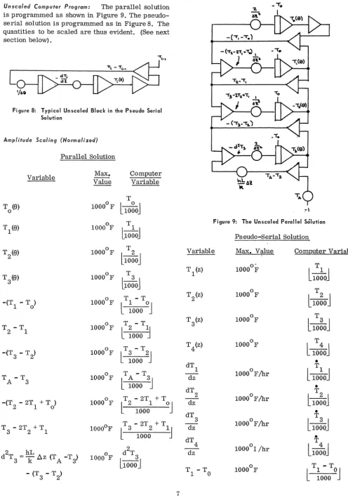
[image:6.612.57.562.61.760.2]Unsealed Computer Program: The parallel solution is programmed as shown in Figure 9. The pseudo-serial solution is programmed as in Figure 8. The quantities to be scaled are thus evident. (See next section below).
~-'
L~
'/,.8
Figure 8: Typical Unsealed Block in the Pseudo Serial Solution
Amplitude Scaling (Normalized)
Parallel Solution
Variable Max. Computer
Value Variable
T
T (9) 10000F
bo~oj
°
T 1 (9) 10000F T1
~oooj
T 2(9) 10000 F T2
L1000j
T 3(9) 10000 F T3
lioooj
-(T - T ) 10000F T -T
1
°
l ~ooo
OJT2 - T1 10000F T - T
t
~ooo
j
-(T - T )
3 2 1000
0F T3 - T2
llOOO
J
TA - T3 10000F TA - T3
t
1000J
-(T - 2T + T ) 10000F T - 2T + T
[ 2 1 oJ
2 1
°
1000T3 - 2T2 + T1 10000F T 3 -2T 2 +T1
l
1000j
d2T
2 hL
. °
d T 3
=
k
6.z (T A -T 3) 1000 F 3L1000J - (T - T )
3 2
,,.\
Figure 9: The Unsealed Parallel Solution
Pseudo-Serial Solution
Variable Max. Value Computer Variable
T 1 (z) 10000
F
T1l1000J
T 2(z) 10000 F T2
[1000J
T 3(z) 10000 F T3 .
[lOOOJ
T 4(z) 10000F
l
T4 1000J
•
dT 1
10000F/hr T1
dz l1000j
•
dT 2
10000 F/hr T2
dz tlOOO-j
•
dT3
°
T3dz
1000 F/hr [1000-j•
dT4 T4
10000 I/hr
l1000J dz
T1 - TO 10000 F
l
T1 ~ TOJ [image:7.620.58.555.61.774.2]Variable
T -T
2 1
T -T
4 3
Pseudo-Serial Solution (Continued)
Max. Value Computer Variable
The scaled equations (not repeated here) are identical to equations (7) through (14) except that a factor of 1/1000 appears on both sides of each equation. This is due to the 1/1000 scale factor which appears in both the variables and their derivatives.
Time Scaling: Since computer time represents
time, (8), for the parallel solution integrators,
while it must, simultaneously, represent distance, (z), for the pseudo-serial solution, there are two "time scale" factors,
.Bj
andt\.
The run time isno longer arbitrary since it represents z, and any
change of the run \time will require rescaling. In
addition, the constants involved in equation (1) are normally stated in terms of units such that time is measured in hours rather than seconds. These factors must be born in mind when trying to inter-pret the. computer program.
The two "time scale" factors, f3j and8i, are
de-termined as follows. Since T =
f3
je
where Tiscomputer time in seconds, then T =0.24~t where t
is real time in hours (recall A = 0 .24t). If we let
0.24Pj = 1, then 1 second computer time represents 1 hour real time. Hence, f3j =1/0.24 =4.16 seconds. (Note the unusual units of this time scale factor. This is due to the normalizationofthe system equa-tion, replacing t bye).
For the pseudo-serial solution, T =
f3
iZ. Tode-termine f3i, it is necessary to know how long a run
is needed for the parallel solution and adjust f3i accordingly so that when z = 1, f3iz equals the run
time. It is anticipated that six hours will be the
maximum period of interest: hence, T = 6 seconds
when z = 1. Therefore, f3i =6 seconds. (Again note the units of 8i).
Note that since there are four stations in space (j = 0, 1, 2, 3), Az = 1/3. In time, (8), there are five stations (i = 0, 1, 2, 3, 4) but the computer
doesn't know this. There are only 4 dynamic
blocks in the pseudo-serial solution, corresponding
to i = 1, 2, 3,4 only since for i = 0 the Ti (z) function is simply a constant representing the original uni-form temperature distribution in the slab. Hence,
/j 8 must be 1/3 of whatever
e
value is representedby 6 hours of real time, namely 8 = 0.24t = (0.24)
(6) =1.44. Hnece, /je =(1.44)(1/3) =0.48.
To summarize:
8j = 4.16 sec (1 sec. computer time
= 1 hour real time)
8i 6 sec (1 sec. computer time
= 1/6 slab thickness
= O.5'~
/jz = 1/3 dim. less (4 stations in space)
/je
=
0.48 dim. less (4 effective stations intime)
The selection of the OP period in the RO moeje is not arbitrary (since run time equals distance for the pseudo- serial solution). Since activating the TR-48 Time Scale bus (DES-30 FAST/NORMAL switch in FAST) causes a 500:1 speed up in solu-tion rate, the OP period must be 6/500 seconds or 12 milliseconds.
The time scale factors are implemented, of course, by manipulating integrator gains rather than writing time-scaled equations.
HOW THE PROGRAM WORKS
Appendix IV shows the detailed program. It is
divided into 3 major functional blocks: Analog Program and Master Timer: Y-Axis Switching and Fast-to-Slow Converter; and, 3-D Plot Control. (The entire diagram can be obtained by combining these three blocks pages on one sheet.)
The system for which this program is written con-sists of the following:
(1) A fully expanded EMC TR-48 (16 integra-tors and 32 amps.), plus two Quad ampli-fier groups (for a total of 36 amps.); with sweep and blanking inputs to the RO scope (allowing it to operate in all modes, not
only RO); pen drop input (logic 1
=
+ 5v=
drop pen): four separate y-axiS to the RO
scope and x, y inputs to the plotter (Yl scope
input not shared with plotter y input); and with 8 electronic comparator units (8 com--parator networks, 16 DA switches, 16 track/
(2) A fully expanded DES-30 with 40 flip flops, 48 AND gates (2-input), 4 down counters, 4 MT-DIF groups, 18 DA trunks, 7 AD trunks.
(3) 1110 plotter
(4) External wide- band oscilloscope for setting the MT and checking the logic program dy-namically.
Analog Program: The parallel solution consists of
integrators 36, 37, 42, 43; amplifiers 24, 25, 40, 41, 28, 29, 32, 33; and pots 45 through 49 and 59.
Pot 04 (with amplifiers 16 and 17) establishes the initial uniform slab temperature To(z) as identical IC's for the integrators of the parallel solution. Thus a convenient control for this parameter is provided.
Pot 49 contains both h (air film coefficient) and k (thermal conductivity of slab) and thus provides control over both.
Pot 59 has on it the cooling air temperature T A'
The pseudo-serial solution consists of integrators 00, 01, 12, 13, 30, 31, 44, 71; amplifiers 04, 02, 15, 19, 47; and pots 03, 00, 16,15,23, 52, 50, 53. Note that P04 provides the function To(z) (a constant) which is needed in the first block of the pseudo-ser-ial solution.
The initial conditions for the h(z) integrators are zero because of the symmetry considerations
al-ready explained. The initial conditions for the
Ti (z) integrators are obtained by the parallel-to-serial IC pickup program which consists of track/ store units, 26, 27, 38, and 65; and GPR 26, AND gates 16A through 16E, and MT6. The function of this program is to sample (and hold) the value
of the temperature as a function of
e
(time) at fourequally-spaced instances of the OP period (cor-responding to i = 1, 2, 3, 4 but not i = 0).
These values are the correct I.C.'s for integra-tors 01, 13, 31, 71 respectively. This is achieved
as follows: The OP period, which is 12
milli-seconds long, is indicated by flip flop 27C being high (this FF is part of the master timer which will be explained shortly). When this is the case, the output of AND gate 16E is four equally-spaced (3 ms apart) blips; the first blip occurs 3 ms after going into OP. These blips are derived from the master timer program. Each time such a blip oc-curs, MT6 generates a 100 microsecond pulse. This pulse is applied to the TRACK ("DIG") input of the track/store units in sequence, beginning with
9
TS-26 down to TS-65. The sequencing is controlled by GPR-26, which is patched as a ring shift regis-ter. During the IC period (FF 27C low), a bit is forced into stage D of this GPR through the L-E
control. Thereafter, each blip that sets MT6 also
shifts this bit one stage ahead. The present posi-tion of this bit determines which of the four AND gates 16A through 16D will transmit the 100 micro-second signal generated by MT6.
A. ,~.
=
,-.
=::::!:I I I IM' • ~~\M". n n n
f"'L--Slit aA --' I
.
-'lit 1.'. s.a. ouc
,.e "U.» L
-AG ,,,. ---1l
"---AGo It-a n
A/lI4.C n
ACi. ,,'0 n
Figure 10: Timing of the Parallel·to.Serial IC Pickup Control
Amplifier 66 is used as a buffer. The low input impedance of the track/store units with the small capacitor causes ringing if the driving amplifier drives 3 or more track/store units simultaneously. Note that amplifiers 36 and 66 drive only two T/S units each.
Master Timer: The function of the master timer is to generate a 12 ms OP - 12 ms IC signals as well as the four equally spaced blips during OP for the parallel-to-serial IC pickup just described. This master timer program consists of down counters 3 and 2, flip flops 27B and 27C, and AND gates 16F and 17F. The function of MT-7 and DIF-7 will be explained shortly; for the time being assume they are removed (Co of DC-2 to Trigger of FF-27C).
AND gate 16-F and FF-27B buffer (clock) the asyn-chronous 1KC square wave source. The output of DIF-6 is a blip every 1 millisecond. DC-3 preset switch is set to 02, so its Co output is a blip every 3 ms (recall that one carry in is required to load the DC with the preset number, during which time EC i is disabled, so the total number of carry-ins per carry-out is the preset number plus one). The Co of DC-3 is thus the signal needed for the parallel-to-serial IC pickup control.
DC-2 counts 3 + 1 =4 of these 3 ms blips, so that
its Co is a blip every 12 ms. This blip may be used to trigger FF-27C so that it is high for 12 ms and low for 12 ms. The outputs of FF-27C can then drive the OP-RST inputs which control the mode of the TR-48.
[image:9.621.326.560.173.246.2]60 microsecond. The reason for this delay will be explained under the fast-to-slow converter description. The delay is achieved by setting MT-7 from the Co of DC-2 and trailing edge differentia-ting (DIF-7) the output of MT-7. Thus the output of DIF-7 is a blip occurring about 60 J.l.s after the Co of DC-2, and it's this differentiator output that is used to trigger FF-27C. Second, in order to assure that the last TRACK signal (the one for TS-65) in the IC pickup program does not extend beyond the OP period, the output of MT-6 is OR'ed in OR gate 18F with the output of FF-27C, and the output of this OR gate is the OP-IC signal. The effect of this modification is felt only at the end of the OP
period; rather than going
to
IC as soon as FF-27Cresets, the TR-48 waits for MT-6 to complete its
100 J.l.s pulse, so that track/store 65 tracks only within the OP period. This is best explained by the timing diagram below. (Figure 11).
• ,. • I I I I I I I I I I
_I~ I I
"'T 1 ~_~_~~~'
__________________
~n~______ __
DI' ,
:1
w:-.21CFigure 11: Master Timer Timing Diagram
AND gates 18D and 18E allow dropping both OP arid RST inputs to logical zero for the HOLD mode. The TR-48 is thrown into HOLD whenever the plot-ter pen is about to be lifted, to prevent streaks. The pen lift operation will be discussed in the 3-D Plot Control section.
The signal out of AND gate 17F is a blip occurring about 60 microseconds prior to going into OP. This signal is labeled MTP (Master Timing Pulse) and is used in the fast-to-slow converter.
Y Axis Switching: Since the plotter will be required
to plot 8 different functions (four parallel and four pseudo-serial solutions), these 8 plots must be switched into the y axis of the plotter in some sequence. (Fast-to-slow conversion must, of course, take place first; this will be described shortly). DA switches 14, 15, 22, 23, 02, 03, 46, 47 accomplish this y-axis-switching. Each switch con-troIs one of the 8 functions and conducts when the
signal on the DA trunk patched into its DIG
(con-trol) input is high (= + 5v). The signals on DA
trunks 0-5, 18, 19 are derived from the 3-D Plot Control which will be explained later.
The switches are patched in a somewhat un-orthodox manner (which may well be the standard configuration in TR-48/DES-30 systems). The
10
input to the switch with its 10K bult-in input re-sistor is not being used at all, since with this low resistor value the switch is non-linear and must be placed in the feedback loop of an amplifier, as shown in the Electronic Comparator Manual; but this implies SPDT operation requiring 2 switches per signal to prevent a no-feedback condition when the
switch is non-conducting. Instead, the GJ (Gate
Junction) input is used with external lOOK resistors. This, incidentally, permits summing into the switch, as shown on switches 14, 15 and 16. The constant voltages summed into these switches in addition to the functions To (8), T1 (8), T2 (8), are bias voltages for 3-D effects. These will be explained in the 3-D Plot Control section. The outputs of the switches ("B") are all patched into the SJ of A23, whose output is minus whichever signal is per-mitted to pass through any conducting DA switch. The "0" point of the DA switches (patched to the amplifier output in SPDT configuration) is not used .
Fast-to-Slow Converter: The function of the
fast-to-slow converter (FSC) is to convert solution shapes produced in RO speeds to identical wave-shapes produced at rates slow enough for plotting. Track/store units 24 and 25 perform this conver-sion. A control signal (the true output of which is patched to TRACK of TS-34 and its complement to TRACK of TS-35) is generated by a "variable-ON-time monostable" (VOTM) program consisting of GPR 21, 14, 20, 15, down counters 0 and 1, and associated flip flop and gates.
The principle of operation of the FSC is this: if the control signal is high from the beginning of the
OP period until time to (where to ~ OP period,
12 ms in this program), then T/S 34 stores the value of the solution at to. T/S 35 begins tracking only when T/S 34 is storing, so its output is also the value of the solution at to. As long as the control signal remains unchanged, the output of T/S 35 remains a constant (this is not true of T/S
34). If the time to is slowly increased (the control
signal remains high for longer portions of the OP period), then the output of T/S 35 will slowly trace the values of the high speed solution.
The three major components of the control signal generation program (VOTM) are: an 8-bit binary down counter, consisting of GPR 21, 14 and gates 12F, 12E, 13E, 13F, 11A, and lOA; an 8-bit binary
up counter, conSisting of GPR 15 and GPR 20; and
a two-decade BCD down counter (DC 0). Note that GPR 15/20 is also patched as a ring shift register, and that GPR 21/14 can accept serial inputs.
DC 0 and FF-29D operate as follows. Every time
[image:10.620.57.282.280.378.2]its carry-out decrements the binary down counter GPR 21/14 and also tries to reset FF-29D through AND gate 12C. As long as GPR 21/14 contain a number other than zero, FF 29D will not reset, so DC 0 reloads itself with 46 and starts counting down again. After GPR 21/14 has been decremented to zero, the Co of DC 0 resets FF29D and stops the counting. The output of FF 29D thus remains
high for a period of 47 (N + 1) microseconds,
where N is the number stored in GPR 21/14 when FF 29D set set.
This number N is loaded into GPR 21/14 serially, before FF 29D is set, from the binary up counter GPR 15/20. This is accomplished as follows. Whenever FF 27D is set, DC 1 counts down 8 clocks and then resets FF 27D. Thus FF 27D out-put is high for exactly 8 clock periods, and this
signal is used to shift the contents of GPR 15/20 into GPR 21/14. The Co of DC 1 (which resets FF 27D and thus stops the shifting) also sets FF 29D which starts the process described in the last paragraph.
The signal that sets FF 27D (thus starting the 8-bit shifting) is either the output of FF 28A or the output of AND gate 19B or 10C. Assume, for the time being, that this signal comes from AND gate 10C, in which case it is the MTP blip from the master timer. (Recall that the MTP indicates the beginning of the OP period, and that it occurs about 60 microseconds prior to the start of the OP period) .
When this is the case, then the sequence of events that take place is as follows:
(1) MTP
(2) GPR 15/20 shift 8 zeros into GPR 21/14
(3) 47 IJ. S microsecond pulse at output of
FF 29D
(4) Wait for next MTP.
Thus, the output of the FSC (T/S 35) is the value of the high speed solution at about 10 microseconds before going into OP; namely this is the IC value.
If, before the next MTP, GPR 15/20 is incremented
(counts up) once, then the sequence above will repeat, except step 2 will read: shift 7 zeros and a 1; and step 3 will read: 94 microsecond pulse,
etc. If GPR 15/20 counts up once before every
MTP, then step 2 in the above sequence will read: shift an 8 bit binary number N into GPR 21/14;
and step 3 will read: 47 (N + 1) microsecond pulse
etc.
11
The incrementing of GPR 15/20 is controlled by FF 27 A, 28A and gates 17E, 18E, and 19E. Assume for the moment that the MTP is routed to AND gate lOB (rather than 10C). The first MTP starts FF 27D - DC 1 as before, this time through AND gate 19B, but it also sets FF 27 A. When the next MTP arrives, it does not pass through AG 19B because FF 27D is set; instead it goes on through AG 17E to set FF 28A and also to increment GPR 15/20 once through OR gate 19E.
If the signal is high, which indicates that the
solu-tion being plotted is one of the pseudo-serial functions, then the output of OG 19E will be high
for ~ clock periods, so it will increment GPR 15/20
twice. In this way the FSC is made to increment
twice as fast as before; this requirement satisfies (partially) the need to Shorten the time base of the pseudo-serial solutions (see 3-D Plot Control explanation). Note that whether GPR 15/20 is incre-mented once or twice, the signal which starts FF 27D and the 8-bit shift (dumping GPR 15/20 contents into GPR 21/14) is the output of FF 28A, so the shifting will not start until the countmg (incrementing) is completed.
The signal that controls the routing of the MTP to AG 10C ("generate FSC control, but do not incre-ment GPR 15/20") is the PEN DROP signal. This
signal, which indicates that the pen is down and ready to plot, is generated by the 3-D Plot Control section. As long as the pen is up, the MTP is routed to AG 10C, and the output of T/S 35 is the IC value. When the pen is down, the MTP goes through AG lOB, GPR 15/20 is incremented on every MTP, and the output of T/S 35 slowly traces the high speed solution.
When GPR 15/20 is full (reading 255), the carry-in from OG 19E causes a carry-out; this Co is the FSC FINish signal, indicating that 1 complete plot has been traced by T/S 35.
The HOLD signal OR'ed into the FSC control Sig-nal (OG 17 A) is generated by the 3-D Plot Control.
It indicates that the pen is in the process of lifting
at the end of the plot; T/S 35 is therefore asked to store (HOLD) so that there are no "streaks" on the paper.
3.D Plot Control: The major components of the 3-D
GPR 22/23 are patched as a ring shift register. Comparator 03 "supervises" the initialization of GPR 22/23 by loading a bit in stage A on the first DES clock, after which the comparator "with-draws". The comparator output is low in PS, so that the complementary output of AD trunk 8 is high, and since the DES is put in RUN before the TR-48 is put in SL, the loading of stage A occurs. Then the TR-48 is put in SL, its mode is cycled between OP and IC by the master timer, comparator 03 out-put is high and AD trunk 8 complementary outout-put is low. The overall effect is as if this situation obtained:
o
The outputs of GPR 22/23 are the signals which control the DA switches in the Y-Axis Switching program previously described. Each time a plot of one function is finished, the EOP (End of One Plot) signal (which will be explained shortly) steps GPR 22/23 and thus selects the next function to be plotted at the input to the FSC (output of A23).
The outputs of GPR 23 are OR'ed in OG llE/llF to generate the signal 0 which signifies that the pseudo-serial solutions are being plotted. This
signal is used in the VOTMprogram. It also causes
DA switch 10 to conduct. This applies the output of integrator 20 to the y-axis to achieve the 45°-line (z-axis) effect, since when switch 10 is conducting, the output of integrator 20 is applied simultaneously to the x and y axes.
Comparator 11 simply acts as an inverter saving a DA trunk which would otherwise be needed to
send
"5
to the TR-48. When 0 = 1, the sum of thecomparator inputs is +4 volts (pot 14 is set to 0.1) so its complementary output is low; when
o
= 0, the comparator input is -1 volt and itscom-plementary output is high. Thus DA switch 11 is
non-conducting when 0 = 1, reducing the time base
integration rate when the pseudo-serial solutions are plotted as explained previously.
The outputs of GPR 22/23 are also used to generate the x-axis bias for each plot. However, since the outputs of the DA trunks are only approximately + 5v when the input is logical 1 and only approxi-mately 0 volts when the input is zero, the pots (25, 26, 27, 28, 40, 43, 42) must be set so that the out-put of A22 gives the correct bias. In addition P29
12
is added so that when all switches are off, it can be adjusted to make A22 output actually zero volts.
The plotting process is started by pushing MP 4C. This sets FF 29C, whose complementary output, the STOP signal, becomes low. FF 28B is also set at the same time, causing the plotter pen to drop. Integrator 20 starts integrating (provide x-axis time base), since the output of OG lIB is low and the complementary output of OG llC/llD is high (OP input
=
1, IC input=
0 on integrator 20).The plotting proceeds until the FSC FIN signal arrives, indicating the completion of one plot. This resets FF 28B (pen up) and sets FF 28C (HOLD mode).
The HOLD mode is retained for about 1 second as follows. FF 29A is enabled by the differentiated 1 CPS square wave. When FF 28C goes high, FF 29A waits for the next 1 CPS blip from DIF 9, and then it goes high until the next 1 CPS blip. FF 28C resets on the same blip that resets FF 29A, so that its output is guaranteed to be high for at least 1 second, and possibly up to 2 seconds (this latter situation occurs when the output of 28C goes high just after 1 CPS blip).
The blip that resets the HOLD flip flop also goes
through AG 19A as the EOP signal - End of One
Plot - which steps GPR 22/23 and also resets the VOTM program so it's ready for the next plot. In addition EOP goes through AG 18C to set MT 9 which generates a 0.5 second (appx.) signal. This signal throws A20 into IC. At the end of the 0.5 second delay, trailing edge differentiator 8 sets FF 28B (pen down) again, and the process repeats.
If LP 5B is depressed, the complementary output
of AG 17B is low. This prevents FF 29C from being reset, so that the plotting process will continue
indefinitely. If LP 5B is released, then when the
bit in GPR 22/23 returns to stage A after completing
8 plots, it causes the next EOP signal to reset
FF 29C rather than set MT 9, thus stopping the process.
REFERENCES
1) Carlson, A.: Investigation of Transient Heat
Conduction; EAI E&T Memo. #9, 2-20-63.
2) Mc Adams, W.H.: Heat Transmission; McGraw
Hill 1954. Page 52.
3) TR-48 Electronic Comparator (Model 40.488)
APPENDIX I: BOUNDARY EQUATIONS
The "parallel" equation at the center of the slab is
dTo T1 -2To +T_1
de
(~z)2But T-1 =Tl by symmetry, hence
The equation at the air-glass interface is
dT3
de
(7)
where T4 is an imaginary point outside the slab. T4 can be obtained from the heat transfer equation across the glass-air interface:
13
by replacing
OZ
and
by then
2~z '
(6.:)2
(h~ ~z
[TA-T3] - [T 3-T2J)
st"t
"'1"0 \.0
-I
st
$C", J' "T
TO .1000 --!.
._-l
'A«ALLtL &oL"'TIO~)E:i~GK
AMPLI'FI,&e,I&"I~
- 'liD \ O'TMEAIoIIS£, GA.N "I.APPENDIX II: STATIC TEST
~ PAItA~L.L-",O-M"·A\"
I Co 11'. C Ie U PC.",,, 'fIlOL..
~M"NUAL\"'"
LOAC> .... I 131''1 S .N E";'fI.'(STOI\Ge i AL~o \ ) . " 0 .... 6<:.'1' tvlT (, ouTPU" l- RGPL"CI::. av LOG' G I 'Fo~ GAT" S
ICoA - 1(; I> .
ELECTRONIC ASSOCIATES INC. RESEARCH AND COMPUTATION DIY.
Box 582, Princeton, N.J.
TR -48 AMPLIFIER ASSIGNMENT SHEET
AOO- A23
PROBLEM _.:::3_-..::t):...;? __ L::.:O __ \' __ .. ~\ ~...::.c;. _ _ _ _
DATE _ _ _ _ _ _ _ _ _ _ _ _ _ _
STATIC CHECK
AMP OUTPUT
NO. FB VARIABLE CALCULATED MEASURED NOTES
CHECK PT. OUTPUT CHECK PT. OUTPUT
00
S
- T,
tT:) /1000 +.o3q.,~ - I01
S
"(%) /1000 .... 1"(.1 ... Cj02 \1\1" _ "(~) 1.000 -.~
c. 03
*-
HI " I-t04
't
( ",(~)
-"To l'fr) )/1000
- .105 INV
_ '-a(e)
/1000 T.c:I06
5
Seol' Eo s,.,eEP07
"N"
- FSC. 08Y
'f A'JII$ IIolPI>T09 ~ X A'\(15 IIJPU,
'5
yf
T/"f;. - "1'0 (&) 11000 ]e= 4A9 +\
Q.,,,t:>
e-Ii ~
S
P.
12
S
- 72,
('l:);'00.,
+.'~'1'~ -\ 13r
"2.(~)
/lrJOO +.\(.,,' - I14
1:
62-"1
)/1000 Tt~) -.115 INII - "'2.(%) /U)O 0 +\
16 INv ' 0('1)/'000 +1
17
",N
- To (i) /1000 -I18
Z.
(""3
-1'2, )/1 000
...
\'-.
19 IN II - 7
a
('i;)/IOOO +.920
S
"Tl1ne e.A$6~ lilly'
T/I(fB)~ooO
-I ~\lAJ)22
L
)C A"jCI~ BIAS23 $1'. F SG 1111 PO"T
M653
ELECTRONIC ASSOCIATES INC. RESEARCH AND COMPUTATION DIY.
Box 582, Princeton, N.J.
TR - 48 AMPLIFIER ASSIGNMENT SHEET A24-A47
DATE _ _ _ _ _ _ _ _ _ _ _ _ __ PROBLEM
_---=3::;.-_l);;...;..P..:;L.;:.0..;. • ..;..T..;...;..;.N~u=_ _ _ STATIC CHECK
AMP OUTPUT
NO. FB VARIABLE CALCULATED MEASURED NOTES
CHECK PT. OUTPUT CHECK PT. OUTPUT
24 ~ _(T,
-'0
)/1000 -.125 INV -'0(9)/1000 +\
26
Tis
- To (9)/'000J 9:: 49 .... 127
TI.s
- lo(9)/i00O]9:'Ue -to I
28 ~ (13 - 2T'2.+T
J
/1000 ... '2.29
L
- ('3 -''3, )
/1000 -.130
S
- ';'3 ('t) /1000 +"~'I1S" - 151
S
13(:C)/IDOO+.''''''1
-.~2
32 2: -d T3
-·S""
33
"Z.
(TAo - T3 ) /'000 +\34
'TIs
fSC.35
Tis
rSC.36
I
'0(9)/1000 + ....32 .. -\
37
I
'T,(9) /1000 -.4:32.4-.9
--,
38
Tis
-T.(9) /1000] 6= 's49 +139 It.lv - T, Ce) /1000 +.C3
40
"L
_(Tl-:2:1'1 "".)/100 0 -+."2.,41
I.
(.'3. -'T, ') /1000 -.\42
J
- Ta(e) /1000 - • .432.4 +J43
S
'.see)
/1000 +.;a'150'*
- .g44
S
- +4
Cil)
/1000 +.O?>4'~ -I'1 I
~ ~
TtJ,(z.)(looo-1-.
I""
'1
- I(tVAt)
46
!
('4-'3 )/ltJOO -.1ELECTRONIC ASSOCIATES INC.
RESEARCH AND COMPUTATION DIV. Box 582, Princeton, N.J.
TR-48 POTENTIOMETER ASSIGNMENT SHEET
POQ-P29
DATE ___________________________ ___ PROBLEM ___ ~_-_O ___ P_L_O_T_i __ I_~_6 ________ __
SETTING STATIC SETTING
POT PARAMETER CHECK POT
NO DESCRIPTION STATIC OUTPUT RUN NOTES NO
CHECK VOLTAGE NUMBER I
00 I / tp~ - . I"", . I te(, i 00
01 01
02 02
03
\ /cPi.
ae) - .0~4'l~ .34'~ 0304 T.(i.) /1000 - I 1.0000 PARA)II&T 6~ 04
05 $Co"PE. SwEll" C w ,DTt\) -. ~lDo .320'0 /'JO "'I .. A I. - Ao:ru~-r 05
06 Sc.o.~ $""E1.6P (ORIGoII'3) -4-1 1.0000
..
..
0607 07
08 08
09 09
10 'TIMa &A6& .... 0""0 .0'1'50 10
II 3AY + .1000 • ~ooo JI),,""U"'I- II
12 12
13 I~
14 0.\ -.1000 ·1000:> COft)6T-""" 61"'$ 14
15
'/~i.
- .1'''' .1("(' , 1516 \fi~i. 68) 16
17 17
18
K
.4000 &~'D"e, liSe. CD~"AOL. 310. 1.61161- 1819 19
20 -rIME aA~6 +.O'lSO .0"750 20
21
4Y
+.'."0 .10 ....".I".,NA
I- 2122 lAy +.2.000 ."2ODO
"
2223
'I
((J, 69) ... 0341'.34,r
2~24 lAy +.)ODO ·aooo ,J 24
25 .6.~ • .2.000 d ItEoucr;: +6\1 ~.14. "1'0 4'lv &KJ -;25
26 lA't .4000
"
II " ,I II -+'1" " 2627 (3Alt ) / 1 0 .0(.00
"
- .1"
"
"
-+'v II 2728 4& lID .'0310 II
..
"
"
..
... I.i II 2829 "lERO ~E.T .. IlO,,, .. T '1'. lD'Ve. AU.wo
"',1'M
29 M654ELECTRONIC ASSOCIATES INC.
RESEARCH AND COMPUTATION DIY. Box 582, Princeton, N.J.
TR-48 POTENTIOMETER ASSIGNMENT SHEET
P30- P59
DATE __________________________ ___ PROBLEM -..,;~;..-_D~_P_L_O_,. __ \ __ \ N---..:G~ ___ _
SETTING STATIC SETTING
POT PARAMETER CHECK POT
NO DESCRIPTION STATIC OUTPUT RUN NOTES NO
CHECK VOLTAGE NUMBER I
30 30
31 31
32 32
33 33
34 34
35 35
36 36
37 37
38 38
39 39
40 2.~e .C::6o<) a6 ."c.~ N ... S., To +3v &_C.T 40
-_
...'-,--41 41
42 4tJ.~/,o •• 200 , ... c IC.E. A££> ... ",.. oj. s'V T<> ... (,,,
'is'''''''
4243 3tJ.9 .1100
"
II..
.\ 'r" ... 4.'5 01 ElI-l>t.T 4344 44
45
'/C'O
6'1~
P->,j ) - .041>'2.4 .2"2. 4546 1/(10 Ai.& ~j) + .O4l'24 ·').1("2 46
47
'/(10
Ai~ ~.i) +.04';S'Z.4 . '2.' (,"2- 4748
'/('0
4,i2. ~ j ) - ~t'Z~O .'1.IC. '2 4849
(hLjk)U
+.(,"1.7 . t.t.t. 1 PAAAMQT"f:R 4950
'/C'i.
Ae)
-.O34'~.3"'S
5051 51
52
' / f3i.
-. ,r.",
.
,,,,,,
5253
'/~i
- . 11.1.'
. ,,,c..1
5354 54
55 55
56 56
57 57
58 58
59 TA /1000 • 10 DO -.\01)0 .4500 PA~AfVI'''E.R 59
M663
,
.-~--...
---~
'i:j 'i:j
t<j
z:
tJ
!;!
H
~
~
t-3
I
I ;
t-<l
'i:j
!
i
i~~E---l--~-I / ; !
;;::::""
i
j014 I
-r
.
~~~~~ ··7~~: -- i-~-~-·-·-~
..
---f---~~-- I I
!
H 0
~ ~
;:0
t<j
ill
-c-~--l c:::: ~
t-3
.~
:~ I
.;;;zr I :
.:r
i IIrf£-~~-#'- ~-;-~- -~~ - --~- -:-~ - - l---~-