ANALOG/HYBRID COMPUTING SYSTEM
ANALOG/HYBRID COMPUTING SYSTEM
RELATED PUBLICATIONS
The table below lists other publications which ma.y be of interest to the readers of this manual. Unless otherwise indicated by title or footnote, all are maintenance handbooks. Note that main-tenance handbooks directly applicable to a particular system are normally supplied with the sys-tem.
Title
Handbook of Analog Computation Basics of Parallel Hybrid Computation 580 Reference Handbook
580 Console Components Manual 580 Computing Components Manual 580 Logic Expansion Group
580/680 Digital Voltmeter, Model 26.268 TR20/TR48 Repetitive Operation Display Units,
Models 34. 034 and 34. 035
NOTIC E
In order to enable us to process your requests for spare parts and replacement items quickly and efficiently, we request your conformance with the following procedure:
1. Please specify the type number and serial number of the basic unit as well as the EAI part number and de-scription of the part when inquiring about replacement items such as potentiometer assemblies or cups, re-lays, transformers, precision resistors, etc. 2. When inquiring about items as servo multipliers,
re-solvers, networks, printed circuit assemblies, etc., please specify the serial numbers of the major equip-ment with which the units are to be used, such as: Console, Type 8811, Memory Module, Type 4.204, Serial No. 000, etc. If at all possible, please in-clude the purchase order or the EAI project number under which the equipment was originally procured.
Your cooperation in supplying the required information will speed the proceSSing of your requests and aid in assuring that the correct items are supplied.
It is the policy of Electronic Associates, Inc. to supply equipment patterned as closely as possi-ble to the requirements of the individual customer. This is accomplished, without incurring the prohibitive costs of custom design, by substituting new components, modifying standard com-ponents, etc., wherever necessary to expedite conformance with requirements. As a result, this instruction manual, which has been written to cover standard equipment, may not entirely concur in its content with the equipment supplied. It is felt, however, that a technically quali-fied person will find the manual a fully adequate guide in understanding, operating, and main-taining the equipment actually supplied.
UNITED STATES AND CANADIAN OPERATIONS
EASTERN REGION
Marketing Division SALES OFFICE
Eastern Reaional Office: West Long Branch, N. J. 07764, Tel: 201-229-1100, TWX 710-722-6597, Telex 01-26655, Cable: PACE West Long Branch. N. J. 07764
Special System Department: West Long Branch, N. J. 07764, Tel: 201-229-1100, TWX 710-722-6597, Telex 01-26655, Cable: PACE West Long Branch, N. J. 07764
Customer Services: West Long Branch, N. J. 07764, Tel: 201-229-1100, TWX 710-722-6597, Telex 01-26655, Cable: PACE West Long Branch, N. J. 07764
Northeastern District Office: 875 Providence Highway, Dedham, Massachusetts 02026, Tel: 617-326-6756
Syracuse District Office: Pickard Building, Room 144-147, 5858 East Malloy Road, Syracuse, New York 13211, Tel: 315-455-5521
SOUTHEASTERN REGION
Southeastern Regional Office: 12260 Wilkins Avenue, Rockville, Maryland 20852, Tel: 301-933-4100 CENTRAL REGION
Central Regional Office: 33166 Des Plaines Ave., Des Plaines, Illinois 60018, Tel: 312-296-8171 Cleveland District Office: 6741 Ridge Road, Parma, Ohio 44129, Tel: 216-842-1840 SOUTHERN REGION
Southern Regional Office: 3514 Cedar Springs Road, Room 211, Dallas, Texas 75219, Tel: 214-528-4920 Houston District Office: 7007 Gulf Freeway, Room 128, Houston, Texas 77017, Tel: 713-MI 4-3678
~~I~~J~I!~8~!;~~~t Office: Holiday Office Center, Suite 2, 3322. South Memorial Parkway, Huntsville, Alabama 35801, WESTERN REGION
Western Regional Office: 1500 East Imperial Highway, EI Segundo, California 90245, Tel: 213-322-3124, TWX 910-348-6284 San Francisco District Office: 4151 Middlefield Road. Palo Alto. California 94303. Tel: 415-321-0363, TWX 910-373-1241 Northwestern District Office: 1107 Northeast 45th St., Room 323, Seattle, Washington 98105, Tel: 206-632-7470
CUSTOMER SERVICES OFFICES EASTERN REGION
Eastern U.S. Headquarters: West Long Branch, N. J. 07764, Tel: 201-229-1100, TWX 710-722-6597, Telex 01-26655, Cable: PACE West Long Branch, N. J. 07764
Northeastern District Office: 875 Providence Highway, Dedham, Massachusetts 02026, Telephone: 617-326-6756 Princeton, New Jersey: U.S. Route No. I, P.O. Box 582, Princeton, New Jersey 08541, Telephone: 609-452-2900 Resident Field Engineers: Bedford, Mass./Florham Park, N. J./Washington, D. C./Baltimore, Md./Eatontown, N. J. SOUTHEASTE~N REGION
Southeastern Regional Office: 12260 Wilkins Avenue, Rockville, Maryland 20852, Telephone: 301-933-4100 CENTRAL REGION
Central Regional Office: 3166 Des Plaines Avenue, Des Plaines, Illinois 60018, Telephone: 312-296-8171 Cleveland District Office: 6741 Ridge Road, Parma, Ohio 44129, Telephone: 216-842-1840
Resident Field Engineers: Detroit, Michigan/Pittsburgh, Pennsylvania/Dayton, Ohio/Warren, Michigan SOUTHERN REGION
Southern Regional Office: 3514 Cedar Springs Road, Room 211, Dallas, Texas 75219, Telephone: 214-528-4920 Houston District Office: 7007 Gulf Freeway, Room 128, Houston, Texas 77017, Tel: 713-MI 4-3678
Huntsville District Office: Holiday Office Center, Suite 2, 3322 South Memorial Parkway, Huntsville, Alabama 35801, Telephone: 205-881-7031
Resident Field Engineers: San Antonio, Texas/Alamogordo, New Mexico/Tulsa, Oklahoma/Houston, Texas WESTERN REGION
Western U.S. Headquarters: CUSTOMER REPAIR FACILITY, 1500 East Imperial Highwa/, EI Segundo, California 90245, Telephone: 213-322-3220, TWX 910-348-6284
Western U.S. Headquarters: CUSTOMER SERVICES FACILITY, 1500 East Imperial Highway, EI Segundo, California 90245, Telephone: 213-322-3220, TWX 910-348-6284
San Francisco District Office: 4151 Middlefield Road, Palo Alto, California 94303, Tel: 415-321-0363, TWX 910-373-1241 Resident Field Eneineers: Edwards, California/Pasadena, California/Moffet Field, California/Martin Marietta Corp., Denver, Colorado/Ryan Aeronautical, San Diego, California
CANADA
Toronto Office: Allan Crawford Associates, ltd., 65 Martin Ross Avenue, Downsview OntariO, Canada, Tel: 416-636-4910 ANALYSIS AND COMPUTATION CENTERS
Princeton Analysis and Computation Center: U.S. Route No. I, P. O. Box 582, Princeton, New Jersey 08541, Telephone: 609· 452-2900
Los Angeles Analysis and Computation Center: 1500 East Imperial Highway, EI Segundo, California 90245, Telephone: 213-322-3220, TWX 910-348-6284
San Francisco Analysis and Computation Center: 4151 Middlefield Road, Palo Alto, California 94303, Tel: 415-321-0363, TWX 910-373-1241
Washington, D. C. Analysis and Computation Center: 12260 Wi IKins Avenue, Rockville, Maryland 20852, Tel: 301-933·4100 Houston Analysis and Computation Center: 7007 Gulf Freeway, Room 128, Houston, Texas 77017, Tel: 713 MI 4·3678
Engineering and Manufacturing Division
Engineerine Department: West Long Branch, N. J. 07764, Tel: 201-229-1100, TWX 710-722-6597, Telex 01-26655, Cable: PACE West Long 8ranch, N. J. 07764
Manufacturing Department: West Long Branch, N. J. 07764, Tel: 201-229-1100, TWX 710-722-6597, Telex 01-26655, Cable: PACE West Long Branch, N. J. 07764
Other Departments, Divisions and Subsidiaries
Instrument Division: Long Branch, N. J. 07740, Tel. 201-229-4400, TWX 710-722-6597, Cable: PACE West Lone Branch, N. J. 07740
Pacific Data Systems, Inc.: 644 Young Street, Santa Ana, California 92705, Tel. 714-540-3610, TWX 714.546-3049 Scientific Instruments Department: 4151 Middlefield Road, Palo Alto, California 94303, Tel: 415·321·7801; TWX 910-373·1241
INTERNATIONAL SALES & CUSTOMER SERVICES OFFICES UNITED KINGDOM & SCANDINAVIA
Electronic Associates, Ltd.: Burgess Hill, Sussex, England, Tel: Burgess Hill (Sussex) 5101·10, 5201-5, Telex: 87183, Cable: PACE Burgess Hill
Northern Area Office: Roberts House, Manchester Road, Altrincham, Cheshire, Tel: Altrincham 5426 SWEDEN
EAI·Electronic Associates·AB: Hagavagen 14, Solna 3, Sweden, Tel: Stockholm 82-40-96; 82·40·97, 83·38-60, Telex Stockholm 10064, Cable: PACE STOCKHOLM
EUROPEAN CONTINENT
EAI·European Continental Regional Office: Centre International, 22nd Floor, Place Rogier, Brussels I, Belgium, Tel: Brussels 18-40-04, Telex: 2.21-106, Cable: PACEBELG Brussels
FRANCE
EAI Electronic Associates SARL: 72-74, rue de la Tombe Issoire, Paris 14e, France, Tel: 535.01.07, Telex 27610 GERMANY
EAI·Electronic Associates GMBH: 5100 Aachen, Bergdriesch 37, West Germany, Tel: Aachen 26042; 26041, Telex 832.676 eai d AUSTRALIA & NEW ZEALAND
EAI·Electronic Associates, Pty., Ltd.: 26 Albany St., Leonards, N.S.W. Australia, Tel: 43-7522, Cable: PACEAUS, Sydney Victorian Office: 34 Queens Road, Melbourne S. C. 2, Australia, Tel: 26-1329, Cable: PACEAUS, Melbourne
JAPAN
EAI·Electronic Associates (Japan), Inc.: 9th Mori Building, 1·3 Shiba-Atago-cho, Minato·Ku, Tokyo, Japan, Tel: 433-4671, Telex: 7814285, Cable: EAIJAPACE
ENGINEERING AND MANUFACTURING
~~~~ro;~cR~~~O~i~r~L. Ltd.: Burgess Hill, Sussex, England, Tel: Burgess Hill (Sussex) 5101-10, 5201·5, Telex: 87183, Cable:
MEXICO
EAI·Electronic ASSOCiates, S.A. de C.V.: Darwin #142, Planta Baja, Col. Anzures, Mexico 5, D.F., Tel: 28-55-13, Cable: PACEMEX
COMPUTATION CENTERS
CONTENTS
CHAPTER 1 - GENERAL DESCRIPTION AND OPERATION OF THE 580 ANALOG/HYBRID COMPUTING SYSTEM
1.1 'GENERAL DESCRIPTION •..•.•••.•.•.••.•.••••••.
1.2 OPERATING CONSIDERATIONS
1-1
1-1
1.3 KEYBOARD PANEL .. • . • • . • • • • • • • • • • • • • • • • . . . . • • • 1-14
1.4 ANALOG READOUT PANEL ••.••••.•••.•••.•...•..• 1-21
1.5 THE AUXILIARY CONTROL PANEL •....•••••.•.•.•. 1-21
1.6 THE LOGIC-CONTROL AND INDICATOR PANEL ••••.•• 1-25
1.7 READOUT DEVICES 1-28
CHAPTER 2 - OPERATIONAL AMPLIFIERS
2 . 1 INTRODUCTION ...•...•....•...•...•... 2-1
2.2 DUAL DC AMPLIFIER PATCHING 2-1
2.3 QUAD DC AMPLIFIER PATCHING 2-4
CHAPTER 3 - ATTENUATORS AND FEEDBACK LTIMITERS
3. 1 ATTE'NUATORS 3-1
3.2 FEEDBACK LIMITER 3-1
CHAPTER 4 - INTEGRATORS
4.1 INTRODUCTION 4-1
4.2 INTEGRATOR TRAYS 4-1
CHAPTER 5 - QUARTER-SQUARE MULTIPLIERS
5. 1 INTRODUCTION .•..•...•••••.•.••...•.••... 0 • • • 5-1
5.2 MODEL 0.7.0146 AND 0.7.0148 QUARTER-SQUARE
MULTIPLIERS ....•.•.•.•.•.•.•.•••.•••....• 5-1
CONTENTS (Cont)
CHAPTER 6 - LOG X DIODE FUNCTION GENERATORS
6. 1 INTRODUCTION .•••.•.•.••.••••.••••••.••.••.•.
6.2 OPERATING CONSIDERATIONS
6.3 OPERATING INSTRUCTIONS
...
'... .
CHAPTER 7 - THE TRACK-STORE, D/ A SWITCH TRAY
7.1 INTRODUCTION
7.2 THE TRACK-STORE CIRCUIT •••••.••••••••••••.•.
7.3 TIlE D/A SWITCH .•.•.•.•••••...••.•.•.•..•..•.
CHAPTER 8 - THE MDFG
8.1 INTRODUCTION
8.2 LOCATION AND ADDRESSING •.•....•••••••••.••••
e.3
APPLICATIONS8.4 SETUP PROCEDURE
CHAPTER 9 - COMPARATORS
AND
FUNCTION RELAYS9 . 1 INTRODUCTION ....•.•..•••...•.••.•.•.•..•.•..
9 • 2 THE COMPARATOR
9.3 FUNCTION RELAYS
CHAPTER 10 - CONTROL TRAY
6-1
6-1
6-1
7-1
7-1
7-1
8-1
8-1
8-1
8-1
9-1
9-1
9-1
CONTENTS (Cant)
CHAPTER 10 - CONTROL TRAY (Continued)
10.2 DVM PATCH TERMINAL ....•••••..•...••.••.•.•.. 10-1
10.3 VM PATCH TERMINAL
10.4 IC AND OP PATCH TERMINALS 10.5 SCOPE PATCH TERMINALS
10.6 PLOTTER PATCH TERMINALS
10.7 CHT ON PATCH TERMINALS
10.8 RDAC PATCH TERMINAL
10.9 A SEL PATCH TERMINAL
10.10 TIMER PATCH TERMINALS
10-1
10-1
10-3
10-3
10-3
10-3
10-3
10-3
10.11 OVD, ORR, AND OLS PATCH TERMINALS •..•.•.•... 10-4
10.12 PP PATCH TERMINAL ..•...•...•...•.••..•. 10-4
APPENDIX 1 - SIMPLE CIRCUITS USING AMPLIFIERS AND ATTENUATORS A1-1
APPENDIX 2 UNITY SCALING . . . A2-1
APPENDIX 3 - TRANSFER FUNCTION SIMULATION ...••...
0...
A3-1APPENDIX 4 - REPRESENTATION OF CONSTRAINTS AND NONLINEARITIES A4-1
APPENDIX 5 - LOGIC PATCHING
APPENDIX 6 - BIBLIOGRAPHY
A5-1
Figure Number 1.1 1.2 1.3 1.4 1.5 1.6 1.7 1.8 1.9 1.10 1.11 1.12 1.13 1.14 1.15 1.16 2.1 2.2 2.3 3.1 ILLUSTRATIONS Title
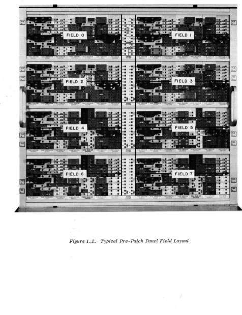
580 Analog/Hybrid Computing System Typical Pre-Patch Panel Field Layout
.I
Physical Layout of the 580 Computer
Amplifiers with Four-Pin Bottle Plugs Providing
Feedback ••.••••••••••..••••••.•••••••••.••••
DVM Zero Adjustment Location Pre-Patch Panel Insertion
Amplifier Balance Control Locations
Computer Component - Field Assignment Areas Removal of Computing Component
Patching Block Replacement ..••••••••••.•••.•••
Keyboard ...•..••.•..•...••••..•..•....••.•....
Analog Readout Panel Auxiliary Control Panel
Logic Control and Indicator Panel Digital Patch ·Panel
Readout Device Connectors
580 Operational Amplifiers (Patch Block Layout and Simplified Schematics) •••.••••.•••••.••• Dual Amplifier, Typical Patching Configurations Quad Amplifier Patching Configuration
Figure Number 3.2 3.3 3.4 3.5 4.-1 4.2 4.3 5.1 5.2 5.3
5.4 .
5.5 5.6 5.7 5.8 6.1 6.2 7.1 7.2
ILLUSTRATIONS (Cont)
Potentiometer Configurations 3-3
Feedback Limiter Patching Block • • 0 • • • • • • • • • • • • 3-5
Typical Limiter Patching 3-5·
Limit Curve 3-6
Integrator Patching Blocks 4-2
Typical Integrator Patching 4-3
Integrator Used as a D/A Switch 4-5
Quarter-Square Multiplier Patch Blocks 5-2
Quarter-Square Mu~~ip1ier, Simplified Diagram 5-3
Multiplier Patching for Multiplication
...
5-4Multiplier Patching for Division
...
5-5Multiplier Patching for Squaring (Two Squaring
Circuits Shown)
...
5-6Multiplier Patching for Square Root 5-7
Multiplier Patching for Multiplication 5-9
Multiplier Patching for Division 5-10
Log X DFG, Simplified Schematic and Patch Block 6-2
Log X DFG Patching 6-3
Track/Store, D/A Switch Patch Block 7-2
Figure Number 7.3 7.4 8.1 8.2 8.3 8.4 8.5 8.6 8.7 8.8 9.1 9.2 10.1
ILLUSTRATIONS (Cont)
Title
Tis
Patching (Typical)D/A Switch Patching (Typical)
MDFG Patching Terminations
Typical Ten-Segment Function
Effect of Changing Slope Pot 5 on DFG Output
DFG Setup Panel (Lower DFG Drawer)
Upper DFG Drawer
Typical Function Requiring Slope Amplification
Initially Horizontal Eleven-Segment Function .•
A Typical Twenty-Segment Function
Comparator and Function Relay Pa'tching Area
Typical Comparator Patching
Control Tray Patch Panel
CHAPTER 1
GENERAL DESCRIPTION AND OPERATION OF THE
580 ANALOG/HYBRID COMPUTING SYSTEM
1.1 GENERAL DESCRIPTION
The EAI 580 Analog/Hybrid Computing System (Figure 1.1) is composed of solid state computing components. The 580 (categorized as a desk-top computer) is compact in size and operates with stability and precision in a normal office or classroom environment as well as a computer laboratory. Each component has input and output terminations on the computer pre-patch panel for inter-connection by bottle plugs and patch cords. The pre-patch panel is arranged in a series of 8 similar patching fields (Figure 1.2), with each field separated horizontally by either a control or trunk trays. The modular design tends to eliminate patching clutter caused by long across-the-panel patching.
The main control panel is located to the lower left of the analog patch panel (Figure 1.3). This area contains a majority of the operating controls.
The analog readout panel, located to the far left of the analog patch panel, contains the overload indicators, DVM readout (an expansion) and a multi-range voltmeter.
The Auxiliary Control Panel, immediately to the left of the analog patch panel, includes 10 handset potentiometers, and override controls for both the compar-ators and the function relays.
The area below the analog patch panel contains two manual diode function generator (MDFG) drawers. The lower drawer contains the set-up amplifier and controls, and up to four, 10-segment MDFGs. The upper drawer is used to house additional segments as required.
The logic package, located at the upper left of the analog patch panel, con-tains the logic patch panel and various indicators and controls for the logic components.
1 • .2 OPERATING CONS IDERATIONS
1.2.1 General
The 580 is completely tested and calibrated at the time of manufacture and is shipped with all components in place. After performing the installation check-out procedure check-outlined in the 580 Maintenance Manual, the computer is ready for operation.
ANALOG
READOUT
PANEL
LOGIC PATCH PANEL
ANALOG PATCH PANEL
Figure 1.3. Physical Layout oj the 580 Computer
MDFG
advertant1y patched to ground or to each other. (Dangling patch cords rarely short to ground because of the plastic patching blocks and because the metal strips between the patching block are covered with a scratch-resistant, non-conductive paint.)
1.2.2 Preliminary Operating Considerations
The following steps are recommended prior to operating the 580 to prevent possible false trouble indications.
1. Be sure that all operational amplifiers have four-pin bottle plugs properly placed and seated as shown in Figure 1.4. This provides the amplifier with feedback. The procedure for inserting and removing the pre-patch panel is described in Paragraph 1.2.3.
2. Turn. the computer on and depress the SP (set pot) button. Initially, the overload lamps of the operational amplifiers will light due to transients; after a few seconds, all of the lamps should extinguish.
3. Check the various supply voltages of the 580. All power supply outputs are connected directly to the voltmeter FUNCTION switch (through appropriate scaling resistors); thus, the check may be accomplished simply and rapidly. (See Paragraph 1.3.5 of this section.)
4. Allow a few minutes warm-up (at least 1/2 hour for the DVM)
time to assure that the computing components (including the
DVM) are up to normal operating temperature. Ground the input,termination in "pp" address mode designated DVM on the control tray and adjust the DVM zero control (Figure 1.5) for a +0.000 reading. Should the polarity relay begin to chatter, turn the zero control slightly clockwise until the chatter stops and the indicators retain the +0.000 display. The DVM
zero adjustment should be checked daily. Initially, this ad-justment may be required more frequently due to aging of the components.
5. Closed relay contacts provide a lOOn feedback resistor for the operational amplifiers when in the set pot mode of the com-puter (SP button on the control panel depressed). (This
4-PIN
BOTTLE PLUGS
4-PIN
BOTTLE PLUGS
THESE PINS JUMPERED
DVM ZERO ADJUSTMENT
DVM READOUT
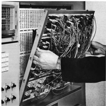
1.2.3 Pre-Patch Panel Insertion and Removal
To insert the pre-patch panel, align the lugs on the bottom of the pre-patch panel frame with the slots in the bottom rail of the patch bay (Figure 1.6). Push the pre-patch panel forward until the lugs on the top of the frame mate with the slots on the top rail of the patch bay. Gently slide the pre-patch panel slightly to the right. Depress the ENG switch. (The computer auto-matically goes into the set pot mode when the ENG switch is depressed.) The patch panel drive system faces the pre-patch panel to the right into the locked position.
Depressing the DIS pushbutton disengages the locking system and forces the pre-patch panel to the left for removal.
1.2.4 Amplifier Balance
'For accurate computation, the operational amplifier must remain balanced. The amplifier must produce a zero output voltage when the combined effects of the input voltages or the absence of input voltages demand it. With this ,require-ment in mind, the amplifiers contain chopper stabilization circuits to minimize
the effect of component drift. Under normal circumstances, the amplifiers do not require balancing for several weeks. However, it is desirable to check this condition periodically; if an amplifier is found to be unbalanced, an adjustment is required. The amplifier balance is checked as follows:
1.2.5
1. Allow a warm-up of 15 to 30 minutes. Place the voltmeter FUNCTION switch in the ABAL position and depress the SP pushbutton of the MODE switch.
2. Use the signal selector system to connect the stabilizer output of each amplifier to the voltmeter. Select AOO and proceed in order. In each case, the voltmeter should reg-ister a deflection that is less than 1/2. division on the meter scale.
3. If an amplifier causes a larger deflection, the amplifier should be balanced. The balance controls for amplifiers are located behind the pre-patch panel on the front block of the amplifiers (Figure 1.7). Adjust these controls for a zero reading on the voltmeter.
Changing Computational Components
In the solution of some problems, it may be necessary to add a computing com-ponent to the existing complement. Since some of the module positions are de-signed to handle more than one type of computing component, a component not required in the problem investigation may be removed and another unit inserted in its place. Figure 1.8 illustrates the various positions of the computing component in the 580 field area. The diagram shows which type of computing component is compatible with each position. The procedure for replacing a
BALANCE CONTROLS
•
•
•
•
•
•
•
•
•
•
•
•
•
•
•
•
(a) 0.6.0614 Dual DC Amplifier
BALANCE CONTROLS
(b) 0.6.0704-2 Quad DC Amplifier
AOO ATTEN A02 A08 ATTEN C AIO ATTEN AI2 Ale ATTEN
POO- A03 P05- 0 N PIO- AI3
P15-P04 P09 T
R PI4 PI9
AMPL INT ---- AMPL MULT AMPL ---- 0 AMPL INT ---- AMPL MULT AMPL
----L
COMPo A04 TIS
TRAY COMPo AI4 TIS
AOI FIR A05 A09 D/A A II FIR AI5 AI9 D/A
A20 ATTEN A22 A28 ATTEN T A30 ATTEN A32 A38 ATTEN
P20- A23 P25- R P30- A33 "'--
P35-U
P24 P29 N P34 P39
AMPL INT ---- AMPL MULT AMPL
----
K AMPL INT ---- AMPl MULT AMPL----S
COMP A24 TIS COMPo A34 TIS
A21 FIR A25 A29 D/A A31 FIR A35 A39 D/A
A40 ATTEN A42 QUAD A48 ATTEN A50 ATTEN A52 QUAD AS8 ATTEN
P40- A43 LOG P45- T R P50- A 53 LOG P55
P44 DFG P49 U P54 DFG P59
AMPL INT
----
AMPL ---- AMPL ---- N AMPL INT ---- AMPL ---- AMPL----MDFG K MOFG
COMP A44 A46 TIS S COMPo A54 A56 TIS
A41 FIR A45 A47 A49 O/A A51 FIR A55 A57 A59 D/A
A60 ATTEN A62 SINEI A68 ATTEN
T A70 AT TEN A72 SINEI A78 AT TEN
P60- A63 COSINE P65- R P70- A73 COSINE P75
P64 P69 U P74 P79
AMPL INT ---- AMPL ---- AMPL ---- N AMPL INT ---- AMPL
----
AMPL----MDFG K MDFG
S
COMP A64 A66 LIMITER COMPo A74 A76 LIMITER
[image:23.615.64.508.59.540.2]A61 FIR A65 A67 A69 A71 FIR A75 A77 A79
1.2.5.1 Computing Module Replacement
1. Remove the pre-patch panel to expose the computing component modules. Remove the two Phillips head re-taining screws from the top and bottom of the module to be removed (Figure 1.9a).
2. Insert the special module extraction tool on the ends of the tray (Figure 1.9b). Pull the tray forward, removing it from the computer.
3. Place the new component in place; be sure the guide pins are properly seated in the guide-pin holes before mating the connectors to the rear of the module.
4. Check that the module is properly installed (connector firmly mated, etc.,) and replace the two retaining screws.
1.2.5.2 Patching Block Replacement
1. The patching blocks of the computing components are held securely in place by the retaining strips on the
front of the pre-patch panel (Figure 1.IOa).
2. The retaining strip above or below the patching block may be removed to change blocks. The retaining strip
is released by removing the four screws directly be-hind the strip on the rear of the pre-patch panel
(Figure 1.lOb). If blocks on two adjacent horizontal rows are to be replaced, remove only the retaining strip between the two rows. The patching blocks can then be removed from the rows above and below the strip.
3. Once the retaining strip is free, remove the original patching block and replace it with the new block (Figure 1.10b). Secure the retaining strip with the four screws. The pre-patch panel is now ready for problem patching.
NOTE
Failure to change the patching block when computing components are changed may prevent proper operation because of the arrangement of the jumpers on
(a) Retaining Screw Location
(a) Removal
(b) Replacement
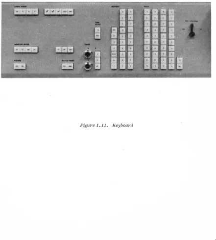
1.3 KEYBOARD PANEL
1.3.1 General
The focal point for control facilities of the 580 is the keyboard panel (Figure 1.11), located to the left of the MDFG drawers. The following paragraphs de-scribe the function and ,use of the various controls and components.
1.3.2 ADDRESS Switch
The ADDRESS switch consists of three vertical rows of pushbutton switches (Figure 1.11). The first row, consisting of seven pushbuttons, is used to select the type of unit to be read out, i.e., A equals Amplifier, P equals Potentiometer. Table 1.1 identifies and describes the function of each switch in this row. The second and third rows contain the tens and units switches respectively. Note that if the position selected is less than 10, the
°
push-button in the 10 column must be depressed. For example, if amplifier 4 in field 0 is to be read out, it has to be addressed as A04.1.3.3 Servo Set Potentiometer Controls (Including RDAC Switches, CL/SET Switches, and the POT CONTROL)
The RDAC switches consist of 4 columns of 10 pushbutton switches with each column labeled 0 through 9. The purpose of these switches is to provide a precise voltage for automatic setting of the Servo set potentiometers.
The CL/SET pushbuttons are used to clear or to ~ an addressed pot once the RDAC pushbuttons have been activated.
The POT CONTROL lever allows adjustment of an addressed pot in any computer mode.
As an example of the operation of the controls described above, assume that a particular pot is to be set to 8 volts. Place the computer in the ~
E2l
mode. Select the pot to be set using the selector system described in Paragraph 1.3.1. Set the RDAC to 8 volts by depressing the 8 pushbutton in the first column and the 0 pushbutton in the second, third and fourth columns. Once the RDAC has been set, depress the SET button and the addressed pot will slew to the proper voltage. If it is necessary to change the value of a pot during problem solution, address the pot and change the value up or down using the POT CONTROL lever.1.3.4 ANALOG MODE Controls
The ANALOG MODE controls are, divided in two types of modes; the computer oper-ating modes and the computer set-up modes. Tables 1.2 and 1.3 indicate the pushbuttons associated with these modes and describes their functions.
1.3,5 PATCH PANEL DIS/ENG Switches
Table 1.1
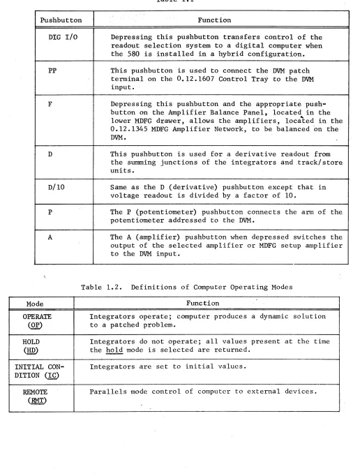
Pushbutton Function
DIG I/O Depressing this pushbutton transfers control of the readout selection system to a digital computer when the 580 is installed in a hybrid configuration.
PP This pushbutton is used to connect the DVM patch terminal on the 08 12.1607 Control Tray to the DVM
input.
F Depressing this pushbutton and the appropriate push-button on the Amplifier Balance Panel, located in the
lower MDFG drawer, allows the amplifiers, located in the 0.12.1345 MDFG Amplifier Network, to be ba lanced 'on the DVM.
D This pushbutton is used for a derivative readout from the summing junctions of the integrators and .track/store units.
D/lO Same as the D (derivative) pushbutton except that in voltage readout is divided by a factor of 10.
P The P (potentiometer) pushbutton connects the arm of the potentiometer addressed to the DVM.
A The A (amplifier) pushbutton when depressed switches the output of the selected amplifier or MDFG setup amplifier to the DVM input.
Table 1.2. Definitions of Computer Operating Modes
Mode Function
OPERATE Integrators operate; computer produces a dynamic solution
(Q£) to a patched problem.
HOLD Integrators do not operate; all values present at the time
(1m) the hold mode is selected are returned.
INITIAL CON- Integrators are set to initial values. DITION (1£)
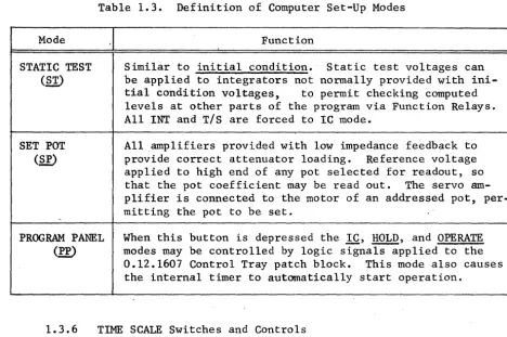
[image:29.612.57.563.45.727.2]Table 1.3. Definition of Computer Set-Up Modes
Mode Function
STATIC TEST
(21)
SET POT
<g)
PROGRAM PANEL
<W
Similar to initial condition. Static test voltages can be applied to integrators not normally provided with ini-tial condition voltages, to permit checking computed levels at other parts of the program via Function Relays. All INT and
TIs
are forced to IC mode.All amplifiers provided with low impedance feedback to provide correct attenuator loading. Reference voltage applied to high end of any pot selected for readout, so that the pot coefficient may be read out. The servo am-plifier is connected to the motor of an addressed pot, per-mitting the pot to be set.
When this button is depressed the IC, HOLD, and OPERATE modes may be controlled by logic signals applied to the 0.12.1607 Control Tray patch block. This mode also causes the internal timer to automatically start operation.
1.3.6 TIME SCALE Switches and Controls
The TIME SCALE and X switches along with the TIMER controls are used to con-trol the analog timer (repetitive operation) circuit. The timer circuit generates the precise time intervals necessary to control the analog modes of the computer for iterative or repetitive operation. The TIME SCALE pushbuttons
p~ovide a 500 to 1 speed-up of the entire computer.
The repetitive operation (Rep-Op) circuit allows both high-speed, and low-speed repetitive operation. Any OPERATE or IC period from 100 ~sec to 100 sec may be selected by the pushbuttons and Vernier controls provided to "bridge the gap" between pushbutton settings. Separate Vernier controls are provided for adjust-ment of the A (IC) and A (OP) periods.
The timer has the following inputs, outputs, and controls:
1.3.6.1 Input. The "RUN" tenninal on the analog patch panel terminates in the control tray in the center of the first row. This input starts and stops the timer, and allows rep-op runs to be terminated by some condition other than elapsed time. For example, if it is desired to operate the analog simulation until some analog variable crosses zero, the RUN input may be patched from a comparator.
[image:30.621.75.543.75.386.2]In ordinary repetitive operation, where the OPERATE period is fixed in advance by the operator, there is no need to patch the RUN input. It is internally connected to the "PP" signal, which is controlled by the ANALOG MODE button labeled "pp" (Paragraph 1.3.3). Thus, ordinary repetitive operation requires no special patching; the operator simply selects the desired A (IC) and A (OP) periods, and depresses the "PP" button. However, if the operator desired to control the timer from an arbitrary logic signal, local patching at the RUN terminal overrides the internal connection.
1.3.6.2 Outputs. The timer has two logic outputs (A and A) and an analog output TB (Time Base). The terminals are connected to the 0.12.1607 Control Tray. The A and
A
outputs normally control the IC and OP buses re-spectively. The IC and OP patch terminals, connected internally to the A andA
terminals, act as inputs to the IC and OP buses. Logic signals at these terminals override the internally generated signals and provide external con-trol of the IC and OP buses.The TB output is an analog ramp generated by an internal integrator and provides a voltage proportional to time. The ramp output may be used to drive the hori-zontal axis of readout devices (Plotting Board, Oscilloscope, etc.,) or may be used as an analog signal for problems requiring a signal proportional to time. The ramp integrates from zero to plus reference voltage during a given operate cycle. Thus, the scaled output is
(tit
),
where t is the length of themax max
operate cycle. (This is a unit scaled notation; the run terminates when t
=
t max' which means (tit )=
1.0 unit, or 10 volts.)max.
1.3.6.3 Controls. The period of the timer is determined by three sets of controls: a pair of dials (one for A, one for
A),
a group of three X (multiplier) pushbuttons (.1, 1, 10), and two TIME SCALE pushbuttons (2 msec, 1 sec). Note that the dials and the multiplier pushbuttons affect the rep-op timer only, while the TIME SCALE pushbuttons control the timer integrator as well as the capacitors in the computer integrators.The A and
X
controls utilize ten-turn Vernier dials with a built-in turn counter. A window at the top of each dial displays an integer representing the number of complete revolutions of the dial~ The graduations around the dial allows a fractional part of a revolution to be set to two figures. Thus, the dial can be set for 5.20 turns, 8.75 turns, etc. The dial has been offset by 0.50 turns. Consequently the minimum position is 0.50 turns while the maximum position is 10.5 turns.The multiplier pushbuttons are a series of momentary contact switches connected in such a manner that when one is depressed it electrically clears any previously selected pushbutton.
A 500 to I speedup of the entire computer is also provided by the TIME SCALE pushbuttons. The TIME SCALE pushbuttons control the time scale relays located in each integrator tray through the time scale bus system. The 500 to 1 speed-up controls both integrators in a dual integrator tray. In the 2 ms range, the time scale bus is at a logic ZERO level energizing the time scale relay. Ener-gizing this relay switches capacitance from 10 ~f to 0.02 ~f, speeding up the problem by a factor of 500. (The problem is automatically rescaled when speeded up by a factor of 500.) The 1 SEC pushbutton switches the time scale bus to a high (+5v) logic level, the relays are de-energized and the computer resumes normal problem speed.
Note that the TIME SCALE pushbuttons only affect the normally patched integrators. By local patching, it is possible to control the time scale input of the inte-grators, located in a particular tray, independent of the master time scale selection system. In addition, it is possible, by local patching, to speed up a factor of 10 to 1 individual integrators.
Table 1.4. Time Periods
TIME SCALE X
(Multiplier) Vernier Time
2 MS XO.l 0.5 to 10.5 100 \-LS to 2 MS
2 MS XI.O 0.5 to 10.5 1 MS to 20 MS
2Ms XlO.O 0.5 to 10.5 10 MS to 200 MS
1 SEC XO.l 0.5 to 10.5 50 MS to 1.0 SEC
1 SEC Xl.O 0.5 to 10.5 0.5 Sec to 10.0 SEC
1 SEC XlO.O 0.5 to 10.5 5.0 Sec to 100.0 SEC
t
1.3.7 POWER Pushbuttons
The POWER pushbuttons control the power for the entire computer. To activate the computer, depress the ON pushbutton. To turn the computer off, depress the OFF pushbutton. The ON pushbutton contains an indicator lamp which lights to indicate that the computer is "ON".
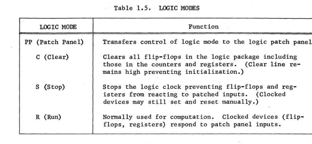
1.3.8 LOGIC MODE Pushbuttons
The LOGIC MODE pushbuttons consist of four momentary pushbutton switches used to control the 580 Logic Package. These switches are connected in such a
manner that when one is depressed it electrically clears any previously selected modes. An indicator lamp in each pushbutton indicates, when lit, which mode is
Table 1.5. LOGIC MODES
LOGIC MODE Function
PP (Patch Panel)
C (Clear)
S (Stop)
R (Run)
Transfers control of logic mode to the logic patch panel.
Clears all flip-flops in the logic package including those in the counters and registers. (Clear line re-mains high preventing initialization.)
Stops the logic clock preventing flip-flops and reg-isters from reacting to patched inputs. (Clocked devices may still set and reset manually.)
Normally used for computation. Clocked devices (flip-flops, registers) respond to patch panel inputs.
1.3.9 Logic Clock Rate Pushbuttons
6 5
The four clock rate pushbuttons (10 , 10 , 10, and STEP) select the clock rate for the synchronized logic elements in the logic package. The pushbuttons are momentary contact switches which, when depressed, select a new6cloc~ rate and electrically clear the previously selected clock rate. The 10 , 10 , and 10 pushbuttons include lamps which indicate which clock rate has been sele~ted.
Table 1.6 lists the function of each clock rate pushbutton.
Table 1.6. Clock Rate Pushbutton Functions
Clock Rate Function
10
STEP
Considered normal clock rate. One clock pulse every micro-second.
One clock pulse every 10 microseconds.
Ten clock pulses every second.
Inhibits all clock pulses when initially depressed. Provides one-clock pulse when subsequently depressed.
1.3.10 Logic RMT (Remote) Pushbutton
[image:33.620.56.561.61.294.2]1.4 THE ANALOG READOUT PANEL
The analog readout panel (Figure 1.12) consists of amplifier OVERLOAD indicators, a multi-range VOLTMETER. A DIGITAL VOLTMETER readout display is also located on this panel if a digital voltmeter (DVM) is provided with the computer. The following paragraphs describe the function and use of the various controls and components.
1.4.1 Amplifier OVERLOAD Indicators
The amplifier OVERLOAD indicators provide a graphic overload display for each individual amplifier. The indicators are numbered (AOO to A79) to correspond with each amplifier position in the computer. The overload indicators are normally extinguished. A lit position indicates that the corresponding
ampli-fier is in an overload condition. During warm-up periods, various overload lamps may light but should be extinguished once the corresponding amplifiers have settled down.
•
1.4.2 The DIGITAL VOLTMETER (DVM) Readout
The DVM readout displays four digits, a polarity sign, and a fifth digit for overrange. The output of any selected amplifier in the coefficient of any selected potentiometer can be displayed on the DVM. The reading may range from ±O.OOOO to ±1.1999 which, when mUltiplied with the reference voltage, represents the voltage into the DVM. As an example a reading of 1.1999 is equivalent to 11.999 volts (UNITS DISPLAYED X REFERENCE VOLTAGE).
1.4.3 The VOLTMETER
The VOLTMETER is controlled by the RANGE and FUNCTION rotary switches located directly below the meter.
The RANGE switch selects the voltage range of the meter. - The ranges provided are: 30, 10, 3, 1, 3, and 0.1 volt for full scale meter deflection. A NULL position is also provided on this switch to convert the VOLTMETER to a null meter.
The FUNCTION switch determines the source of the input signal. Note that many positions on the switch are primarily used for maintenance purposes. However, these positions enable the operator to quickly check all power supply voltages to ensure proper computer operation. Table 1.7 describes the function of each RANGE switch position.
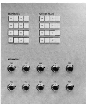
1.5 THE AUXILIARY CONTROL PANEL
The auxiliary control panel (Figure 1.13) contains the pushbutton controls and indicators for the interface components (comparator and function relays), and the ten handset pots (PO through P9).
1.5.1 The COMPARATOR Controls
VOLTMETER RANGE SWITCH
AMPLIFIER """"--.-- OVERLOAD
INDICATORS
DVM ,--.---....,.. READOUT
DISPLAY
~~---~-VOLTMETER
-
-\
0 / , - -' ",.:VOLTMETER FUNCTION SWITCH
COMPAlAto.S FUNCTION .llA YS
...
'"
-POt
-'"
[image:36.618.184.473.151.499.2]comparator output to a particular state regardless of its analog inputs. When the pushbutton is released, the corresponding comparator returns to the state dictated by the patch panel inputs. The numbered pushbutton, when depressed, forces the patch panel output of the corresponding comparator high. Similiarly depressing the blank pushbutton forces the comparator output low.
The numbered pushbutton contains an indicator lamp that lights when the compar-ator output is high. When the comparcompar-ator has a low output the lamp is extinguished.
Table 1.7. VOLTMETER RANGE Switch Functions
Switch Position Function
OFF
PP (Patch Panel)
A BAL (Amplifier Balance) *
S BAL (Stabilizer Balance)*
P SEL
30 (Volts)* 15 (Volts)* 10 (Volts)* 5 (Volts)* -10 (Volts)* -15 (Volts)*
-RV (Relay Volts)*
Disconnects the meter input.
VOLTMETER receives input from VM patch terminal on Control Tray 0.12.1607.
Connects the stabilizer of a selected amplifier to the meter for balancing purposes. Meter deflection should be less than 1/2 division deflection for balanced amplifier.
Connects the stabilizer of either the servo ampli-fier or the ampliampli-fiers on the DFG setup panel to the meter for balancing.
Connects an addressed pot to the meter for setting. This position is used primarily when computer does not contain
a
DVM and is operable only when the RANGE switch is in the NULL position.These switch positions connect the various dc volt-ages in the computer directly to the meter.
*When balancing amplifiers or reading power supply voltages the RANGE switch is inoperative; the appropriate meter ranges are selected automatically.
1.5.2 The FUNCTION RELAY Controls
pushbutton, when depressed, resets the relay. When the pushbutton is released, the function relay returns to the state dictated by the patch panel inputs. If the patch panel inputs are not patched they remain in the state selected by the pushbuttons. Consequently, with no logic signals patched to its inputs, the function relay can be used as a manual function switch controlled by its asso-ciated pushbuttons.
1.5.3 The Handset ATTENUATORS
Ten handset ATTENUATORS (POO to P09) are provided on the auxiliary control panel. Each ATTENUATOR is addressable on the signal selector system and is set in a manner similar to the servo set attenuators except that they are manually
ad-justed. Set each ATTENUATOR to the desired value using the DVM as a readout . device. If the computer does not contain a DVM, the ATTENUATORS have to be set
using the nulling method on the VOLTMETER.
1.6 THE LOGIC CONTROL AND INDICATOR PANEL
The logic control and indicator panel (Figure 1.14) is located at the upper left of the analog patch panel. The panel contains the digital patch panel, AND gate indicators, the REGISTER indicators and pushbutton controls, the in-dicators and thumbwheel controls for the COUNTERS, the general purpose PUSH-BUTTONS and repetitive operation TIME controls (A and
A).
The operation of the various controls and indicators mentioned above are described in the following paragraphs.1.6.1 The Digital Patc~ Panel
The digital patch panel (Figure 1.15) is used to provide access to the inputs and outputs of the logic devices in the logic package. Physically the logic patch panel is divided into four fields (0 through 3) and three trunk areas (0 through
2).
Each of the fields and trunk areas are similar in layout. The particular patching areas and the patch termination functions are described with their associated units.1.6.2 The AND Gate Display
The AND gate display is provided to indicate the output state of each individual AND gate. When the indicator is lit, the output of the gate is high. The
in-dicator is numbered and lettered to correspond to the gates, and in addition, is laid out in the same configuration as the terminations on the patch panel.
1.6.3 The REGISTER Controls and Indicators
REGISTER CONTROLS INDICATORS AND AND INDICATORS THUMBWHEEL SWITCHES
FOR COUNTERS
GENERAL PURPOSE PUSHBUTTONS
REP-OP TIMER CONTROLS
DIGITAL PATCH PANEL
-I'L,D
1
•••••••••••••••••••••••
'iFigure 1.15. Digital Patch Panel
The registers are numbered 0, 1, 2 and 3 while the flip-flops within the reg-isters are numbered in the reverse order. The reverse order of the flip-flops is necessary since, by convention, the most significant bit of a counter is considered to be on the left.
1.6.4 The COUNTER Controls and Indicators
A fully expanded 580 Computer logic package contains four counters which may be used for counting or timing functions. Manual control of the counter is provided by pushbuttons S (set) and R (reset). Pushbutton S contains an in-dicator lamp; it lights whenever the counter output is high.
Depressing pushbutton S sets the output flip-flop and loads the counter. When the count reaches 00, the output flip-flop is reset, and the counter out~ut goes low. The output stays low until the output flip-flop is again set (the counter is loaded). Automatic loading of the counter is accomplished by patching the output through an AND gate (for time delay) to the S patch terminal. The second input for the patched AND gates serves as a controlling input; that is the AND gates can be patched to make the counter operation dependent on two or more separate output functions.
The preset load value is simply a matter of selecting the proper count while the left thumbwheel. represents the tens count. In the event the count is less than 10 (0 through 9) the left thumbwheel is set to zero.
The counter is reset by patching a high to the R (reset) patch ·terminal or de-pressing the manual reset (R) pushbutton on the computer keyboard.
1.6.5 The General Purpose PUSHBUTTONS
The six general purpose PUSHBUTTONS provided in the 580 Computer logic package are latching-type switches whose outputs are terminated on the patch panel. Two pushbutton controls are provided·for each switch. The numbered pushbutton is used to set the switch (output is high), and the adjacent pushbutton (blank) is used to reset the switch (output low). The numbered pushbutton also contains an indicator which, when lit, indicates that the associated output is high. When the output of a PUSHBUTTON is zero, depressing the blank pushbutton
asso-ciated with that output, generates a synchronized pulse (one clock period in length) available at the output terminal.
1.6.6 The TIMER Controls
The rep-op TIMER controls (A and A) are used to manually force the timer into the corresponding mod~s (A
=
IC,A
=
OP). The A pushbutton contains an indicator circuit which lights when the timer is in the IC mode.1.7 READOUT DEVICES
AT ,
-\ii' • •
•
...
,
RECORDER CONNECTOR
(REC-I)
Figure 1.16. Readout Device Connectors
OSCILLOSCOPE
CONNECTOR
(SCOPE-I)
CHAPTER 2
OPERATIONAL AMPLIFIERS
2.1. INTRODUCTION
The operational amplifier is the basic computing element in an analog computer. The amplifier may be used in conjunction with appropriate networks to perform linear computations such as summation, integration, multiplication by a con-stant, and inversion. Accessory components permit use of the amplifier for nonlinear operations such as multiplication and division of variables, and the generation or analytic or arbitrary functions.
There are two amplifiers used in the 580. These are:Dual DC Amplifier, Model 0.6.614-1 and Quad DC Amplifier, Model 6.704-2. Figure 2.1 shows the patch block layout and simplified schematic of each amplifier type and the associated resistor network.
2.2 DUAL DC AMPLIFIER PATCHING
The input and output terminations of the dual amplifier and dual resistor net-works are terminated at the pre-patch panel and are arranged for ease of patching. The nonlinear components are also located in close proximity to the amplifiers for ease of patching and short patch cord runs.
Patching an amplifier for use with an integrator network, or one of the non-linear components, is covered in the separate sections of this manual pertain-ing to the particular component. This section is limited to the description of the amplifier used in conjunction with a resistor network.
Figure 2.2 illustrates two of the more ·common patching arrangements for the Model 0.6.614-1 Amplifier. The patching shown for the upper amplifier (Figure
2.2a) makes use of the standard 4-pin bottle plug and provides the summing circuit shown schematically in Figure 2.2b. This configuration has two gain-of-one and two gain-of-ten inputs. The basic programming symbol for this cir-cuit is shown in Figure 2.2c. Note that the amplifier address number is norm-ally placed in the triangle. Normally, only those inputs to be used are shown.
The lower amplifier (Figure 2.2a) is patched for one of-one and three gain-of-one-tenth inputs using two 2-pin bottle plugs. The simplified schematic and programming symbol for this configuration are illustrated in Figures 2.2d and e. Additional input resistors can be made available by connecting the RJ terminations of different resistor networks together as shown in Figure 2.2f.
Resistors may be patched in series or parallel in the input or feedback circuit to obtain desired gains. Some of these configurations are summarized in
NOTES:
lOOK
I
I
SET POT ~SET POT RELAY BUS
KI
(a) 6.614-1 Dual DC Amplifier Palch Block and Simplified Schematic (One Channel)
10K RJ
IF~O
10K
10
I
.
~IOK
~
10K
10
loon
I
~
I ~g:::SET POT BUS RELAY TO
KI SET POT
. -= RELAY K2
(b) 6. 704-2 Quad DC Amplifier Patch Block
and Simplified Schematic
L SET POT RELAYS SHOWN IN DE-ENERGIZED CONDITION.
4 CONNECTOR BOTTLE PLUG CAN BE USED IN THIS AREA.
2 CONNECTOR BOTTLE PLUGS CAN BE USED IN THESE AREAS.
DUAL AMPLIFIER 0.6.0614-1
(a) Pre-Patch Panel Configuration
RJ~J
0o eo
---
,
10K •
(d) Simplified Schematic (Gain of 0.1 and 1)
lOOK
,
RJ~J
'0
oeo
....
(b) Simplified Schematic (Gain of 1 and 10)
eo =-(O.IXI+0.IX2+0.IX3+X4)
(e) Programming Symbol (Gain of 0.1 and 1)
ADDITIONAL INPUTS
XIW-I
X2 I 'X 10 00 eo
X!
10'eo=-{X I +X2+IOX 3 + IOX4 )
(c) Programming Symbol (Gain of 1 and 10)
(f) Simplified Schematic Showing Additional Inputs
2.3 QUAD DC AMPLIFIER PATCHING
The 580 Computer has provisions for up to eight Quad DC Amplifiers, Model 0.6.704-2 installed in the patch bay. The quad amplifiers have 10K ohm input and feedback resistors for each amplifier circuit. This permits wide band-width, ·low offset, inversion. The 10K ohm resistors are accurately matched to ensure true unity gain inversion. Figure 2.3 shows the normal patch config-uration for one amplifier of a quad.
---'
,---,
RJ;
e.--
J..Ie:
I IL_
IF1e. ___ L _________
c,.'-
:.J.Ie
.,-'
~&.~-QUAD AMPLIFIER
0.6.0704-2
...
4 PIN BOTTLE PLUG - EO= -EIN
CHAPTER 3
ATTENUATORS AND FEEDBACK LIMITERS
3.1 ATTENUATORS
3.1.1 Introduction
The 580 Computers have provisions for 10 handset attenuators (Figure 3.la) and 70 servo set attenuators (Figure 3.lb) when fully expanded. Each row of atten-uators (one row of handset attenatten-uators and seven rows of servo set attenatten-uators) is terminated in a particular field on the patch panel. The first digit in the attenuator address indicates the field number. For example, the handset atten-uators are all terminated in FIELD 0 and are numbered 00 through 09. Each row of the seven rows of servo set attenuators is terminated in a particular field. With the exception of the ungrounded attenuator in each _4 position, all atten-uators in a particular field have one end internally grounded with the ungrounded end and the wiper terminated on the patch panel. The ungrounded pot in each field has both ends and the wiper terminated on the patch panel.
The standard potentiometers are ten-turn, wirewound, 5000 ohm units. The handset attenuators are equipped with vernier di~ls that have a locking mechanism.
3.1.2 Grounded Attenu_ators
Figure 3.2a shows the circuits used in the 580 for setting grounded attenuators under load. Relay·Kl is energized when the cdmputer is placed in set pot mode and applies reference voltage to the high end of all grounded attelluators. Re-lay K2 is energized when the attenuator is addressed by the signal selector system. The wiper voltage is connected to the input of the DVM. The wiper is still connected to the patch panel and is patched to the load it sees when in use. The wiper of the attenuator is adjusted until the desired coefficient is obtained on the DVM.
3.1.3 Ungrounded Attenuators
The operation of the ungrounded attenuators (Figure 3.2b) is similar to the grounded attenuators except that the lower terminal is not internally grounded. Prior to setting an ungrounded attenuator, the lower terminal must be patched to ground. If setting is attempted without the ground connection, the servo drives the attenuator to its highest resistance. The attenuator is held in this position until the CLR pushbutton is depressed and the attenuator is grounded. The ground can be removed from the attenuator once it is set and its address removed.
3Q2 FEEDBACK LIMITER
3.2.1 General
AmNUATOIS
'00
...
,
....
,.
,
POl '0.'06 '07 •• 1 ,.9
~+REF~ _ _ ---4
r - C I - - - _
x
HI
Lo
---t'lo-·.
TO SELECTORSIMPLIFIED CIRCUIT DIAGRAM
KX
SCHEMATIC
(a) Grounded Potentiometer
--Qoo-.. ~ TO SELECTOR
SIMPLIFIED CIRCUIT DIAGRAM
x
HIK(Y-X)+Y
Y Lo
SCHEMATIC
(b) Ungrounded Potentiometer
Figure 3.2. Potentiometer Configurations
COEFFICIENT
~E:TING
X
--k!)---
KX~TENTIOMETER
NUMBER
COMPUTER DIAGRAM SYMBOL
X
K (X-Y)+Y
Y
The 0.42.0342 Module may be installed in any Track/Store potentiometer module slot in the pre-patch panel area. In addition to the l~miter terminations, this module retains the patching terminations for the potentiometer group normally terminated in the area used. The patch block configuration is illustrated in Figure 3.3. The five potentiometers are all available for standard potenti-ometeruse when the limiters are not in use. When the limiters are.in use, the
potentiometers become the limit adjustment controls. When all limiters are used for
±
limiting a sixth attenuator has to be patched from another position.3.2.2 Patching Configuration
Whether used in conjunction with the limiter or not, the five potentiometers can be selected for readout and/or setup using the standard procedure.
Figure 3.4 illustrates a typical patching configuration for the upper limiter of the network. The amplifier to be limited is patched in its normal circuit con-figuration. The limiter is then patched around the amplifier with the LJ to
AJ
and FB to 0 connections as shown. The patching is completed by connecting the Hi-side (top) of two potentiometers to the appropriate reference levels and the wipers to the proper limiter inputs.
3.2.3 Setting the Limit Value
The diode action of the base-emitter junction causes a small amount of "rounding" (or knee) in the amplifier limited output waveform as shown in Figure 3.5. The procedur'e for setting the limiter depends on whether the programmer prefers the knee to fall above or below the limit value. To set the knee below the limit value proceed as follows: Apply reference as the input to the amplifier (opposite in polarity to the output voltage to be limited). Adjust the limit pot to the desired limit value. The knee will start before the limit value is reached, and the amplifier output will not exceed the set value. To set the knee above the limit value proceed as follows: Apply an input that provides the amplifier with an unlimited output equal to the desired limit value. Adjust the limit pot to the point where the limiter just starts to function and then "back-off" the control slightly. The knee will start at the set limit value.
+
HI
O
LJ
e
F8
e
LJ
e
-L
0
+l ( )
-L
0
+ l "POT-LIMITER
0.420342
Figure 3.3. Feedback Limiter Patching Block
(a) Computer Diagram FBO
LJO +LO
(b) Patching Diagram
FBO -LO POT-LIMITER
0.42.0342
LIMIT CURVE KNEE
.
1
~ ~ a..
~
:::) 0
I 2
INPUT~
INTEGRATORS
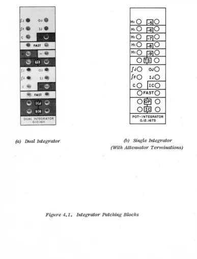
4.1 INTRODUCTION
This chapter includes operating information for the 0.12.1611 Dual Integrator Tray and the 0.12.1675 Potentiometer, Integrator Tray. The patching blocks for these integrators are shown in Figure 4.1. This chapter also includes operation of the repetitive operation group, which controls the integrators when the com-puter is in the rep-op mode.
4.2 INTEGRATOR TRAYS
The 0.12.1611 Dual Integrator Tray and the 0.12.1675 Potentiometer, Integrator Tray are similar except ,that the 0.12.1675 contains only one integrator while
the 0.12.1611 contains two. The operation of each integrator section of each tray is identical. Consequently only th~ dual integrator is discussed in this chapter.
The integrators are typically patched as shown in Figure 4.2. Note that in each field, the integrator trays are physically located adjacent to a dual dc ampli-fier to facilitate the usage of bottle plugs for patching.
4.2.1 Integrator Mode Control
The initial condition (IC), operate (OP), and hold (HD) integrator modes are, controlled by logic signals. The 'table below gives the necessary logic levels at the various control terminals to establish the control modes.
Table 4.1. Integrator Control Modes
IC Input OP Input Resulting Mode
0 1 OP
1 0 IC
0 0 HD
1 1 IC
These modes can be controlled either automatically or manually. The typical patching diagram (Figure 4.2) indicates automatic control utilizing bottle plugs. ,In this method, bottling the OP and IC terminals with a four prong bottle plug
connects the OP and IC terminals to their respective buses. Control of these buses is established at the main control panel and is discussed in Paragraph 1.3.5 of Chapter 1.
(a) Dual Integrator
OJO IJO
cO leO
OFASTO
o
pO
Ole
0
POT-I NTEGRATOR
0.12.1675
(b) Single Integrator
[image:55.615.100.488.185.693.2](With Attenuator Terminations)
TEE BOTTLE PLUG
TWO PRONG BOTTLE PLUG
W'-Wliit-. . .... -+--- TWO PRONG BOTTLE PLUG
~~~~~~~~~~~::~
DUAL AMPLIFIER DUAL INTEGRATOR 0.6.0614-1 0.12.1611
TEE BOTTLE PLUG
IDENTICAL WITH SINGLE INTEGRATOR
TWO PRONG BOTTLE PLUG
[image:56.631.75.489.209.713.2]FOUR PRONG BOTTLE PLUG