users manual
APRIL 1982LSI·11 Bus Interface Chips and Accessories
TECHNICAL VOLUME GROUP 77REED ROAD, HUDSON, MA 01749
The information in this document is subject to change without notice, and should not be construed as a commitment by Digital Equipment Corporation. Digital Equipment Corporation assumes no responsibility for .errors ~hat may appear in this document.
CopYrtght:O. 1979,1981,1982 by Digital Equipment Corporation
.~.
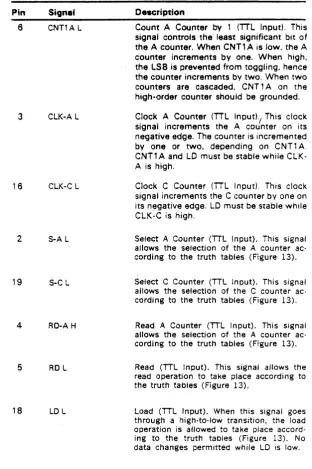
____________________________________________
.. _____
",_,~•• , __ f,,.
'.'1".,
.~•
CONTENTS
ORDERING INFORMATION . . . v
INTRODUCTION ... 1
BRIEF SPECIFICATIONS OF INTEGRATED CIRCUITS .. ... 3
DC003 INTERRUPT LOGIC Description ... 4
Logic Diagram ... 4
Pin Diagram ... 4
Pin/Signal Description ... 5
Electrical Characteristics ... 7
Timing Diagrams ... 12
DC004 PROTOCOL LOGIC Description ... 13
Logic Diagram ... ~' ... 1 3 Pin Diagram ... ' ... '.' ... 13
Pin/Signal Description ... ~ ... 14
Electrical Characteristics ... 1 6 Timing Diagram ... ' ... 21
Loading Configurations ... 21
Timing vs. Loading Table ... 22
DC005 TRANSCEIVER LOGIC Description ... 23
Logic Diagram ... 24
Pin Diagram ... 24
Pin/Signal Description ... 24
Electrical Characteristics ... 26
Timing Diagrams ... 32
DC006 WORD COUNT/BUS ADDRESS LOGIC Description ... 33
Logic Block Diagram ...•... 33
Logic Diagram ... 34
Pin Diagram ... 34
Truth Table ... 34
Pin/Signal Description ... 35
Electrical Characteristics ... 37
Input Voltage Waveform ... 40
Output Voltage Waveform ... 40
Timing Diagram ... 41
Setup Time/Pulse Width Switching Characteristics Table ... 41
DC010 DIRECT MEMORY ACCESS LOGIC
Description ... ~ ... 43
Logic Diagram ... -; ... 43
Pin Diagram ... 43
Truth Table ... 43
Pin/Signal Description ... 44
Electrical Characteristics ... 47
Voltage Waveforms ... 50
Timing Diagrams ... 50
Setup Time/Pulse Width Switching Characteristics Table ... 53
Switching Characteristics Table ... 54
BUS RECEIVERS AND BUS DRIVERS . ... 55
APPLICATIONS General ... 58
Program Control CHIPKIT Application ... 59
DMA CHIPKIT Application ... 67
HARDWARE FOR CHIPKITS General ... 85
Cable BC07D-10 ... 85
Module W9512 ... 86
APPENDIX LSI-11 Bus Timings ... 87
iv
---
...
---~---•
•
ORDERING INFORMATION
Chipkits are designed to provide the design engineer with the material necessary to prototype a new LSI·11 Bus interface. Each kit provides the DEC chips used to implement either a program control (PC) or direct memory access (DMA) interface. The DCK11·AC and DCK11·AD chipkits also provide the W9512 wire wrappable module and interface cable.
LSI·11 Bus Interface chips are sold in several packages depending upon the customer application. A chipkit, as implemented in your custom design, will consist of a combination of up to five different types of DEC-supplied integrated circuits. During your prototyping process you may choose from four types of chipkits. It is often easier to construct initial designs using the chipkits than to build directly from chips. Later, when your design goes int'O volume production, you may save money by implementing the design with individual chips, rather than with the chipkits.
Except where noted, these products are available from the Technical Volume Group of Digital Equipment Corporation and authorized industrial distributors.
The following table describes the chipkits:
Components
Model Number Type DCOO3 DCOO4 DCOO5 DCOO6 DC010 W9512
DCKA11·AA PC 4
DCK11·AB DMA 4 2
.,.
DCK11·AC'" PC 4 ". 1
DCK11·AO* DMA 4 2
The individual chip types used in the chipkits can also be purchasecl in tubes of 18 chips. When purchased this way, volume discounts apply. These discounts significantly reduce the price of production quantities.
The following table lists the chips and their functions:
Model Number Function
DC003·KA Interrupt chip DC004·KA Protocol chip
DC005·KA Transceiver/address decoder/vector select chip DC006·KA Word count/bus address chip
DC010·KA DMA control chips
vi
INTRODUCTION
This Users Manual contains descriptions, specifications, and circuit diagrams for the five integrated circuits available in CHIPKITS for use in LSI-ll bus interlaces. The bus receiver and bus driver chips usually used with the LSI-1I are also covered, and the W95I2 wire wrappable module included with the designers kits is described.
DCKll-AC and AD CHIPKITS include LSI IC chips, a wire wrappable board, and an interface cable.
The DCK11 series of proprietary LSI integrated circuits, developed by DIGITAL for its own use, is now available to LSI-11 users. These ICs, available in sets called CHIPKITS, make design of LSI-11 bus interfaces easier than ever. The kits contain the ICs needed to build the foundation of nearly any LSI·11 interface, and are available either with or without a DIGITAL wire wrappable board and plug-in cable.
The CH IPKITS minimize the chip count required to implement bus circuitry. This permits the designer to build an interface foundation on the double-height wire wrappable board provided, and still have ample room left for his special circuitry. The comparatively small chip count results in backplane space savings, increased system reliability, lower system cost. and a greater opportunity for value to be added by the CH IPKIT customer to the finished product.
DCKll-AC Designers Program Control Bus Interface CHIPKIT, consisting of:
I DC003 Interrupt Chip 1 DC004 Protocol Chip
4 DC005 Transceiver/Address Decoder/Vector Select Chips 1 W9512 Double-height, extended-length, wire wrappable
module
I BC07D-IO ten-foot, 40-conductor plug-in cable
DCKII-AA Program Control Bus Interface CH IPKIT, consisting of thf~ six chips of the above DCKII-AC, but no module or cable.
These kits are ideal for building the foundations of program control bus inter-faces to the LSI-ll. They are functionally similar to DIGITAL's DRVll-P Bus Foundation Module, an assembled, ready-to-use option.
,
DCKll-AD Designers DMA Bus Interface CHIPKIT, consisting of:
DCKll-AB
I DC003 Interrupt Chip I DC004 Protocol Chip
4 DC005 Transceiver/Address Decoder/Vector Select Chips 2 DC006 Word Count/ Bus Address Chips
I DCOIO DMA Control Chip
1 W9512 Double-height, extended-length, wire wrappable module
I BC07D-IO ten-foot, 40-conductor plug-in cable
DMA Bus Interface CH IPKIT, consisting of the nine chips of the above DCKII-AD, but no module 'Or cable.
These kits are ideal for building the foundations of DMA bus interfaces to the LSI-ll. They are functionally similar to DIGITAL's DRVl1 B General Purpose DMA Interface Module.
2
•
Brief Specifications of CHIPKIT Integrated CirCuits Abso'ute Maximum Ratings:
Supp.y Voltage (Vce) +7V Input Voltage (VI) +5.5V
Operating Temp. (Ta) +32°F to + 158°F (O°C to + 70°C) Storage Temp. (Ts) -149°F to +302°F (-65°C to +150°C) Recommended Operating Conditions:
Supply Voltage (Vee) 4.75V (Min.) 5.0V (Norm), 5.25V (Max) Supply Current (Vce) DC003: 140 mA (Max)
DC004, DC005: 120 mA (Max) DC006: 170 mA (Max) DCOIO: 160 mA (Max) Free Air Temperature +32°F to + 1580
F (O°C to
+
70°C) Relative Humidity 10% to 95%, non-condensing Physical Dimensions:DC003, IS-pin DC004,20'pin DC005,20-pin DC006, 20-pin DCOIO, 20-pin W9512 Wire Wrappable Module BC07D-10 Cable
0.3" center DEC 19-12730-00 0.3" center DEC 19-12729-00 0.3" center DEC 1 9-1 3040·00 0.3" center DEC 19-14035·00 0.3" center DEC 19-14038·00
Double height, extended length, single width. 10', 40-conductor ribbon cable, with 40-pin (female) mating connector (H856) installed on one end only; prestripped on other end.
Detailed specifications, circuit diagrams, pin/signal descriptions, and timing diagrams for each IC follow in this Users Manual.
DC003 Interrupt Logic (DEC
# 19-12730-00)
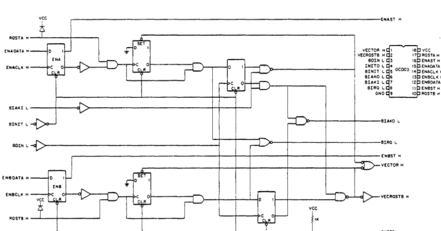
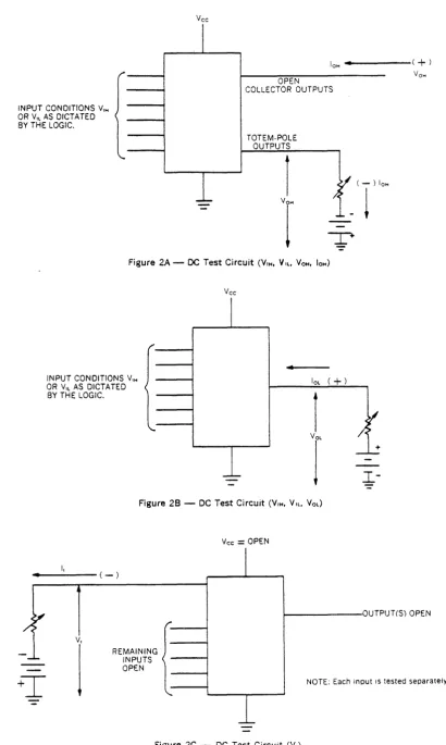
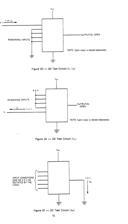
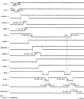
The interrupt chip is an IS-pin. 0.762 cm center X2.349 cm long (max) (0.3 in center X 0.925 in long) dual'in-line-package (DIP) device that provides the circuits to perform an interrupt transaction in a computer system that uses a daisy-chain type of arbitration scheme. The device is used in peripheral interfaces to provide two interrupt channels labeled "A" and "8." with the A section at a higher priority than the 8 $ection. Bus signals use high-impedance input circuits or high current open*col-lector outputs, which allow the device to directly attach to the computer system bus. Maximum current required from the Vec supply is 140 mAo Figure 1 is a simplified logic diagram of the DC003 IC. Figure ,~ shows the test conditions used to derive the data presented in the Electrical Characteristics. Figure 3 shows the timing for the "A" interrupt section while Figure 4 shows the timing for both "A" and "8" interrupt sections. Table 1 describes the signals and pins of the DC003 by pin an(j signal name.
r - - - . - - - E H A S T H
ROSTA H -'""---_+_----~
l
VE~~~~~: ~
ENAOATA ...
SOIN L
EHACLK H
---'-l
IHITO L
,., SINIT L
BlAKO L
I
':::},~
):>--+--- BlAKO L
BIAKl L ---+---<:4 ~---_+_+_--+_--'
BINH L
BOIN L - + - - - B I R Q L
r---r--~~---~----~---_+----EHBST ...
VECTOR H EN80ATA H
EHBCL~ H VECROSTB H
ROSTS H - . l . . - - - I - - - - . . . J IK
~ _ _ _ _ _ _ _ _ _ _ _ _ _ _ _ ~ _ _ _ _ _ _ _ _ _ _ _ _ _ _ _ _ _ _ ~ _ _ _ ~ _ _ _ _ _ ~ _ _ _ _ _ _ _ _ _ _ _ _ _ IHITOL
Figure 1 DC003 Simplified Logic Diagram
...
4
.• • .1 14 . . . . :1::
au ilia;:;;.
iii:;; I ;::: II .. ;;; .. ' Pi iii.; : : Iivee
RQSTA H EHAST H
ENAOATA H
ENACLK H ENBeLK H
ENBOATA H ENBST H
RQSTB t<
[image:11.617.96.544.361.596.2]·_---.~--.
...
"Table 1 OC003 Pfn
I
Signal DescriptionsPin Signa' VECTOR H
2 VECRQSTB H
3
BDIN L4 INITO L
5
BINIT L6
BIAKO L7 BIAKI L
Spec
Group Description
I Interrupt Vector Gating. This signal should be used to gate the appropriate vector ad-dress onto the bus and to form the bus signal called BRPLY L.
Vector Request "8." When asserted, in-dicates RQST "8" service vector address is required. When unasserted, indicates RQST "A" service vector addless is re-quired. VECTOR H is the gating signal for the entire vector address; VECRQS18 H . "; normally bit 2 of the vector address.
111 Bus Data In. This signal. generated by the processor BDIN, always precedes a BIAK signal.
1* Initialize Out. This is the buffered BINIT L signal used in the device interface for general initialization.
III
II
III
Bus Initialize. When asserted. this signal brings all driven lines to their unasserted state (except INITO L),
Bus Interrupt Acknowledge (Out). This signal is the daisy-chained signal that is passed by all devices not requesting inter-rupt service (see BIAKI L). Once passed by a device, it must remain passed until a new BIAKI L is generated.
Bus Interrupt Acknowledge (In). This signal is the processor's response to BIRQ L true. This signal is daisy-chained such that the first requesting device blocks the signal propa-gation while non-requesting devices pass the signal on as BIAKO L to the next device in the chain. The leading edge of BIAKI L causes BIRQ L to be unasserted by the requesting device.
Pin
8
10 17
11
16
12
1513 14
Table I DC003 Pin/Signal Descriptions (Cont)
Signal BIRQ L
RQSTB H RQSTA H
ENBST H ENAST H
Spec
Group
ENBDATA H ENADATA H
ENBCLK H ENAClK H
II
III III
Description
Bus Interrupt Request. This signal is gen-erated when this device needs to inter-rupt the processor. The request is gen· erated by a false to true transition of the RQST signal along with the associated true interrupt enable signal. The request is removed after the acceptance of the BDIN L signal and on the leading edge of the BIAKI L signal or the removal of the associated interrupt enable or the remclval of the associated request signal.
Device Interrupt Request. When asserted with the enable flip·flop set, will cause the assertion of BIRQ L on the bus. This signal line normally remains asserted until the request is serviced.
Interrupt Enable Status. This signal indi-cates the state of the interrupt enc:ble internal flip-flop which is controlled by the signal ENX (where X is either A or B) DATA H and the ENX (where X is either A or B) ClK H clock line.
Interrupt Enable Data. The level on this line, in conjunction with the ENX (where X is either A or B) ClK H signal, deter· mines the state of the internal interrupt enable flop. The output of this flip-flop is monitored by the ENX (where X is either A or B) ST H signal
Interrupt Enable Clock. When asserted (on the positive edge), interrupt enable 1'lip-flop assumes the state of the ENX (where X is either A or B) DATA H signal line.
6
'1IIIIIIII"
- - - -_ _ _ _ _ _ _ _ _ _ _ _ _ _ . - - " , . ~~~i
Specifications
DC003 Electrical Characteristics
DCOO3 TTL (Non-Sus) Interface
(Specification Group I - TTL Input and Output Pins)
Parameter Requirements
Name Symbol Conditions • Min Max Unit
High-level input VIH (See Fig. 2A, 28) 2.0 V voltage
Low-level input V'l (See Fig. 2A, 28) 0.8 V voltage
Input clamp volt- V, Vee
=
4.75 V -1.2 Vage I,
=
-18 mA(See Fig. 2C)
High-level output VOH Vee
=
4.75 V 2.7 Vvoltage 10
=
-1 mA(See Fi g. 2A)
Low-level output VOL Vee
=
4.75 V 0.5 Vvoltage 10
=
20 mA(See Fig. 28)
Input current: at I, Vee
=
5.25 V mAmaximum input V,
=
5.5 Vvoltage (See Fig. 2D)
High-level input 1, ... Vee
=
5.25 V 50 )J.Acurrent V, = 2.7 Vt
(See Fig. 2D)
Low-level input I'L Vee
=
5.25 V -0.55 mAcurrent V,
=
0.5 V:I:(See Fig. 2E)
Short-circuit out- los Vee= 5.25
v§11
-40 -100 mAput current (See Fig. 2f)
Supply current IcC" Vce
=
5.25 V 140 mA (See Fig. 2G)• Ambient operating temperature (T.o.)
=
00to +700
C unless otherwise specified.
t
IrH=
1 00 )J.A at pins 1 2 and 1 5. :I: IIL= -2.0 mA at pins 12 and 15.§ Not more than one output shall be shorted at a time and duration shall not exceed 1 second.
DCOO3 Bus Driver
(Specification Group II - Open Collector) Parameter
Name Symbol Conditionsl
Output reverse current
Low-level output voltage
VOL
Vee = 4.75 V
VOM
=
3.5 V(See Fig. 2A) Vee =4.75 V
ISINK
=
70 mA ISINK=
16 mA(See Fig. 28)
Requirements Min Max Unit
25
0.8 0.5
v
V
lAmbient operating temperature (TA) = 0° to +700 C unless otherwise specified.
DCOO3 Bus Receiver
(Specification Group III - High Input Z)
Parameters Requirements
Name Symbol Conditionsl Min Max Unit
High-level input VIH Vee = 4.75 V 1.53 V
voltage Vee = 5.25 V 1.70 V
(See Fig. 2A, 28)
Low-level input VIL Vee = 4.75 V 1.30 V
voltage Vee = 5.25 V 1.47 V
(See Fig. 2A, 28) Input clamp VI Vee = 4.75 V
voltage II =-18 mA -1.2 V
11=+18mA 6.25 V
(pins 10 and 17 only) (See Fig. 2C) High-level input hH VI = 3.8 V
current Vee = O.V 40 /-LA
(Do not do for pins 10 and 17)
Vee = 5.25 V 40 /-LA
(See Fig. 20) Low-level input IlL VI= OV
current Vee = 0 V -10 /-LA
(Do not do for pins 10 and 17)
Vee = 5.25 V -10 /-LA
(See Fig. 2E)
lAmbient operating temperature (TA)
=
0° to +700C unless otherwise specified.
8
~\
~
---...-,,...-,~, ~,~~""'"j
INPUT CONDITIONS VIH
OR VI~ AS DICTATED BY THE LOGIC.
Vee
101-1 .... ~----(
+ )
OPEN COLLECTOR OUTPUTS
TOTEM·POLE OUTPUTS
1
I
Figure 2A - DC Test Circuit (VII-t, 'IlL. VOM, 10 M)
INPUT CONDITIONS VIH
OR VIL AS DICTATED
BY THE LOGIC.
Vee
..
10L ( + )
1
l'
[image:16.614.114.524.59.744.2]
I-Figure 28 - DC Test Circuit (VIM. VI~, VOL)
...
- - - - ( - )1
REMAINING INPUTS OPEN
Vee
=
OPEN1---OUTPUnS) OPEN
NOTE: Each input is tested separately
(+
)V,
V,
Vee
I
I, or '1104
•
OUTPUnS) OPEN
REMAINING INPUTS
NOTE: Each' Input is tested'separately
==-
1
I-Figure 2D - DC Test Circuit (b. 11M)
Vcr:
I
4.5 V
REMAINING INPUTS
•
"L ( - )INPUT CONDITIONS GND OR 4.5 V AS DICTATES BY THE LOGIC.
NOTE:
1
Figure 2E - DC Test Circuit (Ill)
Vee
1
Figure 2F - DC Test Circuit (los)
10
OUTPUT(S) OPEN
Each input is tested separately
( - )
r
-~
[image:17.613.125.549.38.779.2]INPUT CONDITIONS GND OR 4.5 V AS DICTATED BY THE lOGIC.
+
VeeIJ
-
L-Figure 2G - DC Test Circuit (Icc)
- , 30.0 I 300 ' 81NIT L ~ MIN:
:
:
~5 I~---INITO L ~ C-.J
ENA.QATA I<
ENACLK I< 30MIN_,
Fl
n
I
~---I
ENAST I< 7-30~
F
ROSTA ...
BIRO L
BOIN L
alA"' L 35MIN~ ~
'~-vECTOR ... _ _ _ _ _ _ _ _ _ _ _ 'O_-_4_~_-_,...,r- ~ IL.._'0_-_4_5 ______ - i _ _ -r-____ _
BIAKO L '2-55...
~
': _ 12-55-, I
Figure 3 DC003 "A" Interrupt Section Timing Diagram
- , ~9.9 r300 I BINIT L ~ MIN: , ,
:
,r+i---INITO L -;:;;0, :..J'2-50ENBOATA ...
ENe CLK I<
ENS ST I<
BIRO L
,- .JoIll..:..!:J :
I
I
30MIN-1
~L..--
____-7 - 3 0 - :
F
'5- 65--]
t-
.... ______________________
-J_;.., _ ...F"70---,ROSTB I< _ _ _ _ _ _ _ ~
ENAOATA I<
ENACLK M
EN. ST M
ROSTA H
BOIN L
BIAKI L
J
I
30 MIN
--i
F"lL..-_______________ ... ____ _
I
I I
~--I
35 MIN ~
P,"-
---3-5-M-,N-_--.;...'-F=---r--l_rh
s-tJ'n_~
vECTOR H _ _ _ _ _ _ _ _ _ _ _ _ _ _ _ '0_-_4....:~iI...J ~ t t O .. -45 10,"45}:] :~_5 __ _
I I
~,.
vECROSTB ... _ _ _ _ _ _ _ _ _ _ _ _ _ _ _ _ _ _ _ _ _ _ _ _ _ _ _ _ _ _ _ _ _ _ '_5_"6---'5 c::J :---L:~ NOTE.
T t,"U or ~ In nano •• conGa
Figure 4 DC003 "A" and "S" Interrupt Sections Timing Diagrams
12
11·4151
[image:19.617.163.459.374.721.2]~.
DC004 PROTOCOL LOGIC (DEC #19-12729-00)
The protocol chip is in a 20-pin 0.762 cm center X 2.74 cm long (0.3 in center X
1.08 in long) DIP device that functions as a register selector. providing the signals to control data flow into and out of up to four word registers (eight bytes). Bus signals can directly attach to the device because receivers and drivers are provided on the chip. An RC delay circuit is provided to slow the response of the peripheral interface to data transfer requests. The circuit is designed such that if tight tolerance is not required. then only an external 1 K ±
20 percent resistor is necessary. External RCs can be added to vary the delay (see Table 3). Maximum current required from the Vce supply is 1 20mA. Figure 5 is a simplified logic diagram of the DC004 IC. Signal timing with respect to different loads is shown in Table 3 and in Figure 7. Figure 6 shows the test conditions used while Figure 8 shows the load· ing for the test conditions. Signal and fJlll definitions for the DC004 are
presented in Table 2.
vECTOR H vee NOTE
BOAL2 L ENB H
The pin names shown
-in this SOALI L Rxex H
SOALO L SELO L diagram are for the situation where 8WTBT L SELl L the DCOO4 is connected to the 8SYNC L SEI.4 I. internal 3·state bus of the DCOO5s
eOIN L SEI.S L
9RPLY I.
our La,
not connected directly to the LSI· SOOUT I. 12OuT >t8,
11 bus.GNO 11 !NWO I.
ENBH ... - - - - I
9SYNC I.
BOALl I. ----+-1
SEL 6 L
SEI. 4 L
BOAll L - - - - 1 - 1 0 SEL 2 L
SEL 0 L
SOAlO L ----+--1 ~----~--~~=>---i~~---OUT>tSL
~--~-~=a->---r-i~~---OUTL8, aWTBT L
r - - - " . e x
>t
6RPLY L
SOOUT L
eo IN L >---t~====~~~---(NWOL
VECTOR H - - - '
Pin 2
3
4 5 6 78
9
1 1 12 13Table 2 DC004 Pin/Signal Descriptions Signal
VECTOR H
BOAL2 L BOAL 1 L BOALO L
BWTBT L
BSYNC L
BOIN L
BRPLY L
BOOUT L
INWO L
OUT LB L OUT HB L
Spec Group II II II II II Description
Vector. This input causes BRPLY L to be generated through the delay circuit. Inde-pendent of BSYNC Land ENB H. Bus Data Address Lines. These signals are latched at the assert edge of BSYNC L.
Lines 2 and 1 are decoded for the se~ect outputs: line
0
is used for byte selection. Bus Write/Byte. While the BOOUT L input is asserted. this signal indicates a by tEl or word operation: Asserted=
byte. unas-serted=
word. Decoded with BOOUT L and latched BDALO L to form OUT LB Land OUT HB LBus Synchronize. At the assert edge of this signal. address information is trapped in four latches. While unasserted. disables all outputs except the vector term of BRPL Y L.
II Bus Data In. This' is a strobing signal to
III
II
, effect a data input transaction. Genera tes BRPL Y L through the delay circuit and INWD L
Bus. Reply. This signal is generated through an RC delay by VECTOR H OR'd with BOIN L or BOOUT L and the AND of BSYNC L and latched ENB H.
Bus Data Out. This is a strobing signall to
effect a data output transaction. Decoded with BWTBT Land BOALO to fClrm OUT LB L and OUT H B L Gener61tes BRPLY L through the delay circuit.
In Word. Used to gate Iread) data fronn a selected register onto the data bus. En-abled by BSYNC L and strobed by BOIN L.
Out Low Byte. Out High Byte. Used to load Iwrite) data into the lower. higher, or both bytes of a selected register. Enabled by BSYNC L and decode of BWTBT L 2lnd latched BOALO L. and strobed by SOOUT L
14
Pin 14
15 16
17
18
19
Table 2 DC004 Pin/Signal Descriptions (Cont)
Signal
SELO L SEL2 L SEL4 L SEL6 L
RXCX H
ENS H
·Spec Group
111
1:lI
Description
Select lines. One of these four signals is true as a function of BDAL2 Land BDAL 1 L if EN B H is asserted at the assert edge of BSYNC L. They indicate that a word register has been selected for a data transaction. These signal.s never become asserted except at the assertion of BSYNC L (then only if EN B H is asserted at that time) and once asserted. are not serted until BSYNC L becomes unas-serted.
External Resistor Capacitor Node. This node is provided to vary the delay be-tween the BOIN L, BOOUT L, or VECTOR H inputs and BRPLY L output. The ex· ternal resistor should be tied to Vee and the capacitor to ground. As an output, it is the logical inversion of BRPLY L.
Enable. This signal is latched at the as-serted edge of BSYNC L and is used to enable the select outputs and the address term of BRPLY L.
DC004 Electrical Characteristics
TTL (Non-Bus) Interface
(Specification Group I - TTL Input and Output Pins)
Parameter Requirements
Name Symbol Conditions· Min . Max Unit High·level input V.M (See Fig. 6A, 68) 2.0 V voltage
Low·level input V'L (See Fig. 6A, 68) 0.8 V voltage
Input clamp V. Vee
=
4.75 V -1.2 Vvoltage I. = -18 mA
(See Fig. 6C)
High·level output YOM Vee
=
4.75 V 2.7 Vvoltage 10= -1 mA
(See Fig. 6A)
Low·level output VOL Vee = 4.75 V 0.5 V
voltage 10 = 20 mA
'-~
(See Fig. 68)
Input current at I. Vee = 5.25 V 1 mA maximum input V.
=
5.5 Vtvoltage (See Fig. 60)
High.level input ItM Vee
=
5.25 V 50 JJ.Acurrent VI= 2.7 Vt
(See Fig. 60)
Low-level input IlL Vee
=
5.25 V -0.70 mAcurrent V.
=
0.5 V(See Fig. 6E)
Short·ci rcuit los Vee= 5.25 V+ -40 -100 mA output current (See Fig. 6F)
Supply current lee Vee =5.25 V 120 mA (See Fig. 6G)
* Ambient operating temperature (TA) = 00 to
+700
C unless otherwise specified.
t limits for pin 19 are:
II = 1.40 rnA: IIH = -2.25 rnA min, -3.85 mA max. IlL = -4.5 mA min, -8.0 mA max.
+ Not more than one output shall be shorted at a time and the duration shall not exceed 1 second.
16
..."
OC004 Bus Receiver
(Specification Group II - High Input Z)
Parameter Requirements
Name Symbol Conditions
*
Min Max Unit High-level input VIM Vee=
4.75 V 1.53 Vvoltage Vee
=
5.25 V 1.70 V(See Fig. 6A, 68)
Low-level input V'l Vee
=
4.75 V 1.30 Vvoltage Vee
=
5.25 V 1.47 V(See Fig. 6A, 68)
Input clamp V, Vee
=
4.75 V -1.2 Vvoltage I,
=
-18 mA(See Fig. 6C) High-level input I,M V,
=
3.8 Vcurrent Vee
=
a
V 40 }.LAVee
=
5.25 V 40 }.LA(See Fig. 6D) Low-level input k V,
=
OVcurrent Vee
=
a
V -10 }.LAVee
=
5.25 V -10 }.LA(See Fig. 6£)
* Ambient operating temperature (TA)
=
0° to +70° C unless otherwise specified.DC004 Bus Driver
(Specification Group III - Open Collector) Parameter
Name Symbol Conditions· Output reverse
current
Low-level output voltage
10M
VOL
Vee
=
4.75 V VOM=
3.5 V (See Fig, 6A) Vee=
4:.75 VISINK= 70 mA~ ISINK
=
16 mA~ ISINK=
15 mA§(See Fig. 68)
Requirements Min Max Unit
25t }.LA
0.8 V
0.5 V
0.5 V
* Ambient operating temperature (TA)
=
0° to 70° C unless otherwise specified.INPUT CONDITIONS VI .. OR Vll AS DICTATED BY THE
LOGIC.
lKu..± 5%
Vee
OPEN COLLECTOR
OUTPUTS ...--10 .. (
+ )
Vo ..Vee o---~~v---~~R_X~C~X __ _r----~
1
I
I
Figure 6A DC Test Circuit (VIH. VIL VOH. IOH)
INPUT CONDITIONS VI .. OR
VI AS DICTATED BY LOGIC.
Vee
..
I
lK12± 5%
Figure
( - )
REMAINING INPUTS
OPEN
Vee
10L ( + )
RXCX VOL
j
.l
68
DC Test Circuit (VIM. Vll. VOL)Vee
=
OPENUTPUT(S) OPEN
1 K12:±: 5 %
RXCX 1 - - - ' \ 1 \ / 1 _ - - - 0 Vee
NOTE: Each Input is tested separately
Figure 6C DC Test Circuit (VI)
18
-,
Vee
r IH
•
r--oUTPUT(S) OPEN
REMA INING INPUTS lKIl± 5%
-">AA J"I
'"
RXCX Vee
-L
NOTE: Each input is tested separate IyFigure 60 DC Test Circuit (II, IIHI
Vee
REMAINING INPUTS
(---t
OUTPUT(S) OPEN
1
INPUT CONDITIONS GND OR 4.5 V AS DICTATED BY LOGIC.
lK!l± 5%
RXCX 1 - - - " ' V " w - - - - o V e e
NOTE: Each Input IS tested separately
Figure 6E DC Test Circuit (IlL)
Vee
lK!l± 5%
RXCX . A A A ~
..
'" '" Vee( - ) los
1
1
_
...
INPUT CONDITIONS GND OR 4.5 V AS DICTATED BY THE LOGIC.
( + ) Vee
1
RXCX
-
"--Figure 6G DC Test Circuit (Icc)
20
OUTPUT(S) OPEN
lK!!± 5%
A A A
"v Vee
- - - -_ _ _ _ _ _ _ _ _ _ _ _ _ _ _ _ _ _ _ _ _ _ _ _ _ _ _ _ _ _ _ _ _ _ _ _ _ __ _ _ _ _ _ _ _ _ _ _ _ MM _ _ . -_ _ _ _ _ _ . . __ · ~_ •
BDAI. (2.1.0) I.
??M25
MINlt5MIN~~~~ENe H
@~;;;a ~iN! ~iNW%2?:1;<~~~:_%;·:%
9SYNC I..
SEI. (0.2.4,6) l.
NOTE· BDOUT L
OUTHB t. OUTlS L
9DIN t.
iNWO L
8R.PLY L
VECTOR H
15 MIN,
--i
~r---15-M-I-N.-j-l"":
_ _ _ _I·
I I
~TI2F
I ~ - . I T14-"!": - ; m r--I.. _ _ _ -+_-__
-I: --
2.4 V'd==:J
1=-=11..--_
1 - - - _
6 1-1
i~
--i
fiSt-
'-_________ _
• TIME REQUIRED fO OISCHARGE R, C, FROM ANY CONDITION ASSERTED' I~On.
Time. an In nonos.condl
FROM OUTPUT
Figure 7 DC004 Timing Diagram
Vee
~
O{\,
roo"
LOAD A
OC OUTPUTS
FROM OUTPUT
LOAD 8
TTL OUTPUTS Vee
R2
DIODE -F0777
CONDITION I R2' 280n C2·15pf CONDITION 2
R2' OPEN C2' t60pf
Figure 8 DC004 Loading Configurations for Table 3
Table 3 DCOO4 Signal Timing vs Output Loading
With Output Being Output Being
Respect Condi· Asserted (ns) Negated (ns) Fig. 5
Signal to Signal tion Min Max Min Max Reference
SEL (0.2.4,6) L BSYNC L 2 15 40 :5 30 T5, T6
(Load B)
OUT LB L BOOUT L 2 5 30 :5 30 T9, TI0
(Load B)
OUT HB L BOOUT L 2 5 30 :5 30 T9, TI0
(Load B)
INWO L BOIN L 2 5 30 :5 30 TIl, T12
(Load B),
Pin 18 BRPLY L OUT LB L 20 60 -10 45 T13, T14
Connection (Load A) (Load B)
RX
=
330n
= 5% BRPLY L OUT HB L 1 20 60 -10 45 T13, T14CX
=
IS pF = 5% (Load A) (Load B)BRPLY L INWO L 1 20 60 -10 45 T13, T14
(Load A) (Load B)
BRPLY L VECTOR H 30 70 0 45 T13, T14
(Load A)
Pin 18 BRPLY L OUT LB L 1 300 400 -10 4S T13. T14
Connection (Load A) (Load B)
RX
=
4.64K BRPLY L OUT HB L 1 300 400 -10 45 T13, T14=1% (Load A) (Load B)
CX
=
220 pFBRPLY L INWO L 1 300 400 -10 45 T13, T14
=1%
(Load A) (Load B)
BRPLY L VECTOR H 330 430 0 45 T13, T14
(Load A)
Pin 18 RXCX H OUT LB L 10 50 10 50 TIS, Tl6
Connection
RXCX H } (Load OUT HB L 10 50 10 50 TIS, Tl6
RX
=
330 u=S% RXCX H A) INWO L 10 50 10 50 TIS, TI6
CX
=
IS pF RXCX H VECTOR H 10 50 10 50 TIS, T16=5%
See Figure 8.
22
'---_._---
--"
DC005 TRANSCEIVER LOGIC (DEC
#
19 .. 13040-00) ,
The4-bit transceiver is a 20-pin. 0.762 cm center X2. 74 cm long (0.3 in. center X 1.08 in. long) DIP, low-power Schottky device; its primary use is in peripheral device interfaces to function as a bidirectional buffer between a data bus and peripheral device logic bus. It also includes a comparison circuit for device address. selection and a constant generator for interrupt vector address generation. The bus I/O port provides high-impedance inputs and high drive (70 rnA) open collector outputs to allow direct connection to a computer data bus structure. On the peripheral device side. a bidirectional port is also provided. with standard TTL inputs and 20 rnA. tri-state drivers. Data on this port are the logical inversion of the data on the bus side.
Three address "jumper" inputs are used to compare against three bus inputs to generate the signal MATCH, The MATCH output is open col-lector. which allows the output of several transceivers to be wire-ANDed to form a composite address match signal. The address jumpers can also be put into a third logical state that disables jumpers for "don't care" address bits. In addition to the three address jumper inputs. a fourth high-impedance input line is used to enable/disable the MATCH output.
Three vector jumper inputs are used to generate a constant that can be passed to the computer bus. The three inputs directly drive three of the bus lines. overriding the action of the control lines.
Two control signals are decoded to give three optional states: receive data. transmit data. and disable.
Maximum current required from the
Vee
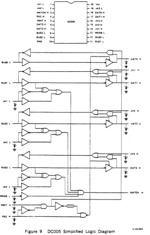
supply is 120 mA.Figure 9· is a simplified logic diagram of the DC005 IC. Timing for the various functions is shown in Figure 11. Signal and pin definitions for the DC005 are presented in Table 4. Figure 10 shows the test condi· tions used to derive the data listed in the Electrical Characteristics.
JAt L 20 Vee
JA2 L 19 JA3 L
MATCH H 3 18 OATO H
REC H 17 OAT1 H XMIT H 5 OCOOS t6 JV] H OAT] H 15 JV2 H OAn H 14 JV1 H
BUS] L 13 MENB L
BUS2 L 12 BUSO L
GNO 10 11 BUSI L
CIATO H
BUSO L
JVl H
BUSI L CIAT1 H
JAI L
JV2 H
BUS2 L C)AT:! H
JA2 L
1---4-I---k'li-r=;:::=rr
J'V3 HBUS3 L >-....L...-+-~ a'ATl H
JA3 L
,---~==1-.;-1---1- MATCH H
XMIT H -r---r~
REC H
...,...-"---Pin
12 1 1
9
8
18
17 7
6
Figure 9 Deaa5 Simplified Logic Diagram IC·OCOOS
Table 4 De006 ~in/Signal Oescriptiona Signal
BU5(3:0) L BUSO L BUS1 L BUS2 L BUS3 L DAT(3:0) H DATO H DAT1 H DAT2 H DAT3 H
Spec· Group
II +111 II
+
III II +111 II+
IIIDescription
Bus Data. This set of four lines constitutes the bus side of the transceiver. Open col-lector outputs; high-impedance inputs. Low
=
1.Peripheral Device Data. These four tri-state lines carry the inverted received data from BUS (3:0) when the transceiver is in the receive mode. When in transmit data mode. the data carried on these lines is passed inverted to BUS (3:0). When in the disabled mode . .these lines go open (HI-Z). High
= ,.
24
..
[image:31.613.178.475.34.499.2]~'
,..,.
Pin 14 15· 16 133
12
195
4Tab'e 4 DCOO5 Pin/Signal Descriptions (Cont)
Signa' JV(3: 1) H JV1 H
JV2 H
JV3 H
MENS L
MATCH H
JA(3:1)L JA1 L JA2 L JA3 L
XMITH
REC H
Spec Group V V V II III IV IV IV Description
Vector Jumpers. These inputs. with inter-. nal pull-down resistorsinter-. directly drive BUS
(3: 1 ). A low or open on the jumper pin will cause an open condition on the corre-sponding bus pin if XMIT H is low. A high will cause a one (low) to be transmitted on the bus pin. Note that BUSO L is not con-trolled by any jumper input.
Match Enable. A Iowan this line will en-able the Match output. A high will force Match low. overriding the match circuit.
Address Match. When BUS (3: 1) match with the state of JA (3: 1) and MENS LIs low. this output is open: otherwise it is low.
Address Jumpers. A strap to ground on these inputs will allow
a
match to occur with a one (low) on the corresponding BUS line: an open will allowa
match with a zero (high):a
strap to VCC will dis-connect the corresponding address bIt from the comparison.Control Inputs. These lines control the op-eration of the transceiver
a
s follows.REC
o
o
XMITo
1o
DISABLE: BUS. OAT open XMIT DATA: OAT - BUS RECEIVE: BUS -> OAT
RECEIVE: BUS - OAT
To avoid 3-state signal overlap conditions. an internal circuit delays the change of modes between XMIT DATA and RECEIVE mode and delays 3-state drivers on the DAT lines from enabling. This action is independent of the DISABLE mode.
25
DCOOS Electrical Characteristics
DeOOS TIL (Non-Bus) Interlace
(Specification Group I - TIL Input and Output Pins)
Parameter Requirements
Name Symbol Conditions * Min Max Unit
High-level input VIM (See Fig. lOA, 2 V
voltage lOB)
Low-level input VIL (See Fig. lOA, 0.8 V
voltage lOB)
Input clamp voltage VI Vee
=
4.75 V -1.2 V I,=
-18 mA(See Fig. 10C)
High-level output YOM Vee
=
4.75 V 3.65 Vvoltage 10
=
-1 rnA(See Fig. lOA)
Low-level output VOL Vee
=
4.75 V 0.5 Vvoltage 10
=
20 rnA(See Fig. lOB)
~
Input current at I, Vee
=
5.25 V 1 mAmaximum input V,
=
5.5 Vvoltage (See Fig. 100)
High-level input IIH Vee
=
5.25 Vcurrent VI
=
2.7 VREC 100 J.LA
XMIT 50 J.LA
(See Fig. 100) Low-level input IlL Vee
=
5.25 Vcurrent VI
=
0.5 VREC -2.2 mA
XMIT -1.1 mA
(See Fig. 10E)
Short-circuit output los Vee
=
5.25 Vt -40 -100 rnAcurrent (See Fig. 10F)
Supply current Icc Vee
=
5.25 V 120 rnA(See Fig. lOG) Off state (high- 1010FFI Vee
=
5.25 Vimpedance state) VI
=
3.65 V 100 J.LAoutput current VI
=
0.5 V -0.36 rnA(OAT pins only)
* Ambient operating temperature (TA)
=
00 to +700 C unless otherwisespecified.
t Not more than one output shall be shorted at a time and the duration shull not exceed 1 second.
.-.
26
---
..
---.
----
..
-"-,
DC005 Bus Receiver
(Specification Group II - High Input Z)
Parameter Requirements
Name Symbol Conditions • Min Max Unit
High-level input VIH Vee = 4.75 V 1.53 V •
voltage Vee = 5.25 V 1.70 V
(See Fig. lOA, lOB)
Low-level input VI~ Vee = 4.75 V 1.30 V
voltage Vee = 5.25 V 1.47 V
(See Fig. lOA, lOB)
Input clamp VI 1,=-18mA -1.2 V
voltage Vee = 4.75 V
(See Fig. 10C) High·level input IIH VI = 3.8 V current (includes
open-collector leakage on bus pins)
MENB Vee = 0 V 40 iJ.A
Vee
=
5.25 V 40 iJ.ABUS Vee
=
0 V 65 iJ.AVee
=
5.25 V 65 iJ.A(See Fig. 100) Low-level input ilL VI
=
0.5 Vcurrent Vee = 0 V -10 iJ.A
Vee = 5.25 V -10 iJ.A
(See Fig. 10E)
,. Ambient operating temperature (T A)
=
00 to +700 C unless otherwise specified.DCOO5 Bus Driver
(Specification Group III - Open Collector) Parameter
Name Symbol Conditions·
High-level output current (reverse current-match output only)
t
Low-level output voltageIOH
VO~
Vee
=
4.75 VVOH
=
5.25 V(See Fig. lOA)
Vee
=
4.75 V IslNIC=
8 mA(Match)
ISINIC
=
70 mA(Bus)
ISINIC
=
16 mA(Bus) (See Fig.lOB)
Requirements Min Max Unit
25
0.5 0.8 0.5
iJ.A
V
V V
• Ambient operating temperature (TA)
=
00 to +700 C unless otherwisespecified.
DCOO5 (Specification Group IV - Ternary State Inputs)
Parameter Requirements
Name Symbol Conditions1 Min Max Unit
Low-level input Vll (See Fig. lOA) 0.3 V voltage
High-level input VIH (See Fig. lOA) 4.75 V voltage
Open circuit input VOP 4.75<Vee 2 V
voltage <5.25
lAmbient operating temperature (TA)
=
00to +700
C unless otherwise specified.
DC005 (Specification Group V - TTL Input with Pull-Down)
Parameter Requirements
Name Symbol Conditions1 Min Max Unit
High-level input VIH (See Fig. lOA) 2 V voltage
Low-level input Vll (See Fig. lOA) 0.8 V voltage
Input clamp VI Vee = 4.75 V -1.2 V
voltage 11= -18 mA
(See Fig. laC)
High-level input IIH Vee = 5.25 V 1.2 mA
current VI = 2.4 V
(See Fig. 100)
Low-level input VII Vee = 4.75 V 0.8 V VOltage forcing Ii = 0.1 mA
input current (See Fig. 10H)
Input current at III Vee = 5 V 50 200 ,.,.A
low·level VI = 0.4 V
(See Fig. 10E) 1Ambient operating temperature (TA) = 00
to +700
C unless otherwise specified.
28
~
Vee
OPEN COLLECTOR
OUTPUTS 10H (
+ )
VOHINPUT CONDITIONS
VIM or VI~ AS DICTATED BY THE LOGIC.
GND
TOTEM·POLE OUTPUTS
l
Figure lOA DC Test Circuit - VIM. VIL, VOH. IOH
INPUT CONDITIONS
VIH or Vil AS
DICTATED BY LOGIC.
Vee
Vee
GNO
..
10L ( + )
Figure 108 DC Test Circuit - VIM. VIL. Vo~
... 1 , _ ( - )
V~r:
( - ) 10
1
I
I
REMAINING INPUTS
OPEN
OUTPUT(S) OPEN
v,
Vee
I
I, or I"
•
Vee-
OUTPUT(S)- ' - - V,
--
REMAININGINPUTS
GND NOTE: Each Input is tested separately
1
.l
Figure 100 DC Test Circuif-II, 11M
Vee
o;l 4.SV
{REMAINING INPUTS
(---4
Vee
OUTPUTS(S) OPEN
INPUT CONDITIONS GND OR 4.SV AS DICTATED BY THE LOGIC.
GND
~ Except Pin 4 and Pin 5 Pin 4
=
Pin 5=
.SV forIlL Test.
NOTE: Each input is tested separately
Figure 10E DC Test Circuit - IlL
Vee
Vee
GND
NOTE: Only one output be shorted at a time and the duration should not exceed more than a second.
Figure 10F DC Test Circuit - los
30
----_
..
_---
--,,,
I,"
+
VeeIcc
INPUT CONDITIONS
GND OR 4,SV AS OUTPUT(S)
DICTATED BY THE OPEN
LOGIC.
•
I
Figure lOG DC Test Circuit - Icc
Vee
Figure lOH DC Test Circuit - VII
TRANSMIT DATA TO BUS
XMIT H _ _ _ _ _ ...11 I
-1
L 5 TO 30.,-I
f-
5 TO 3()n,~EC H (G~OUNOI _____________ r-______________________________ ___ BUS L - OUTPUT
5 TO 25.'-i -l 1
! - ' _ _
-"r--1-5 TO 25.,
OAT H-INPUT
L:_
RECEIVE DATA FROM BUS (BUS INITIALLY HIGH)
X MIT H (GROUND I _______________________________________ _
OAT H -OUTPUT
FlEC H _ _ _ _ _ _ ~_!
I
==l
f-
0 TO 30.1 ,.... _ _ _ _ _ _ _ _ :1 ... _-;1-0 TO 3'0.,HiZ---,
I
L - - _ H i Z::oj
f-
e TO 30.1BUS L-INPUT
- - - . . . - - - - i l
r=-RECEIVE DATA FROM BUS (BUS INITIALLY LOW)
XMIT H (GROUNOI
I
I
-1
I-
0 TO 30nl-1
f-O TO 300nlHiZ---l
I
r - - -
HiZ--1 I-e TO 30., FlEe H
---~
OAT H-OUTPUT
BUS L - INPUT 1
L_
VECTOR TRANSFER TO BUS
I
d
I-
20nl MAX -ir
20n, ~!!..I
JV H
---~
BUS L - OUTPUT
ADDRESS DECODING
X
:j 1-10 TO 40.,
I
X
::j
~
10 TO 40nl-I I-5 TO 40.1 BUS L - INPUT _ _ _ _ _ _ _ _ _ _ _ _ _ _ _ _ __
MATCH H _ _ _ _ _ _ _ _ ...,... __ 0+-______ ---'
MENB L
I
I
RECEIVE MODE LOGIC DELAY
XMIT H
FlEC H
1-40 TO 90.1 OAT [3:01 H 10UTP~;i _ _ _ _ _ _ _ _ _ _ - - J1
Figure 11 DeDOS Timing Diagram
32
- - - -_ _ _ _ _ _ _ _ _ _ _ _ _ _ _ _ _ _ _ _ _ ...-._~ ... ...iio.-. . . '""
DC006_WORD COUNT/BUS ADDRESS LOGIC
(DEC
#
19-14035-00)
The word count/bus address (WC/BA) chip is a 20·pin, 0.762 cm center X 2.74 cm long (0.3 in center X 1.08 in long) DIP, low·power Schottky device. Its primary use is in DMA peripheral device interfaces. This IC is designed to connect to the 3-state side ot the DCOOS transceiver. The DC006 has two a·bit binary up·counters, one for the word (byte) count and another for bus address. Two DC006 les may be cascaded to increase register implementation.
The chip is controlled by the address latch protocol chip (DC004), the DMA chip (DCOlO), and a minimum of ancillary logic. Both counters may be cleared simultaneously. Each counter is sepa~ately loaded by LD and the corresponding select line from the protocol chip. Each counter is incremented separately. The we counter (word byte counter) is always incremented by one; the A counter (bus address) may be incremented by one or two for byte or word addressing, respectively.
Data from the DC006 IC is placed on the 3-state bus via internal 3-state drivers. Each counter is separately read by RD and the corresponding select line.
Figure 12 is a block diagram of the DC006 IC while Figure 13 illustrates a simplified logic diagram. Figures 15 and 16 illustrate input and output voltage waveforms. Figure 17 shows the timing diagram of the DC006 while the setup time and pulse width switching characteristics are pre-sented in Tables 6 and 7. The De006 pin/signal description is presented in Table 5. Figure 14 shows the various test conditions employed to derive the data presented in the t7:Jectrical Characteristics.
CNT1 A ( ) - ! - - - - t - - t - - ' - i
ClK·A ( ) . . . - l - - - - t - - t - - ' - i
1 . 0 0 - + - - - - 1
S·A
S·C
AD·A Q - I - - - i
RD ( ) - ! - - - - f
READ CONTROL 1.0GIC
MAX·A CLK·C
Figure 12 DC006 Simplified Block Diagram
33
CNnA L
ClK·A L
SOC l
S-A L
RO l
RD-A H
LO L
ClK-C H
TRUTH TABLES WHERE
INPUTS LO H RD-A RD
L L
L L
L L
L L
L H
H L
H L
H L
H L
H H
H H
H H
H H
INPUTS RD '" - L RD - H
LD t t t X H H H
• liL LOW • liL HIGH • DON'T CARE - HIGH IMPEDANCE - HIGH TO LOW TRANSITION
READ CONTROL
OUTPUTS
s-A s-C [lIF<7:0>
L L CLEAR A&C AND READ C L H A<7:0> H L C<7:0>
H H Z
X X Z
L L CLEAR A&C AND REAO A L H A<7.0> H L "'<7:0> H H "'<7:0> L L CLEAR A&C AND READ A L H "'<7:0> H L "'<7.0> H H A<7:0>
WRITE CONTROL
FUNCTION s-", SoC
L L *llLEGAL L H LOAO "'<7:0> H L LOAD C<7:0> H H WC SA NOT SELECTED L l CLEAR BOTH COUNTERS L H LOADING DISABLED H L LOADING DISABLED
*IlLEGAL CONOITION BECAUSE A LOAO OPERATION AND A CLEAR OPERATION IS AliEMPTED SIMULTANEOUSLY RESULT OF THIS CONDITION IS CLEAR.
CNT1 A H MAXA ~ 01 02 ClKA L 03
04
ClR H 05
06
A COUNTER 07 B BfT BINARY UP COUNTER
lDA H
O/F (0:7)
C COUNTER B BIT BINARY UP COUNTER 00
01
02
lOC H 03 04 05
ClKC l 06 07 ClR H
MAXC L
D/F(0:7)
MAX-A H S-A L
RD L
1 DIF H
2 OIF H 4 DIF H GND
}O?l
i }
CI.?IFigure 13 DC006 Simplified LogiC Diagram
34
VCC s-CL LD L MAX-C ~I ClK-C L 12BD/F ,~ 64D/F H 32D/F H
180/F H SDIF H
{ ? - - M A X - A H
DF7
-12BO/F H
840/F H
320/F H
160/F H
BO/F H
40/F H
20/F H
10/F H
{ > - - M A X . C H
[image:41.616.174.446.78.315.2]---
..
--...
~
----,
Pin
6
3
16
2
19
4
5
18
Table 5 DC006 Pin/Signal Descriptions
Sign ••
CNT1 A L
AD-A H
AD L
LD L
Oescription
Count A Counter by 1 (TTL Input). This signal controls the least significant bit of the A counter. When CNT1 A is low. the A counter increments by one. When high. the lSa is prevented from toggling. hence the counter increments by two. When two counters are cascaded. CNT 1 A on the high·order counter should be grounded. Clock A Counter (TTL Input)"! This clock signal increments the A counter on its negative edge. The counter is incremented by one or two. depending on CNT 1 A. CNT1 A and lD must be stable while
ClK-A is high.
Clock C Counter (TTL Input). This clock signal increments the C counter by one on its negative edge. LD must be stable while CLK-C is high.
Select A Counter (TIL Input). This signal allows the selection of the A counter ac· cording to the truth tables (Figure 13).
Select C Counter (TIL Input). This signal allows the selection of the C counter ac· cording to the truth tables (Figure 13).
Read A Counter (TIL Input). This Signal allows the selection of the A counter ac· cording to the truth tables (Figure 13).
Read (TTL Input). This signal allows the read operation to take place according to the truth tables (Figure 13).
[image:42.611.140.453.204.674.2]Table 5 DC006 Pin/Signal Descriptions (Cont)
Pin Signal 7 -9 DfF (7:0) H
11-15
MAX-A H
17 MAX-C H
Description
Data Bus (Bidirectional, 3-State Outputs/ TIL Inputs). These eight bidirectional lines are used to carry data in and out of the selected counter.
Maximum A Count (TIL Output). This sig-nal is generated by ANDing CLK-A and the maximum count condition of counter A (count 376 when counting by 2 or count 377 when counting by 1).
Maximum C Count (TIL Output). This sig-nal is generated by ANDing CLK·C and the maximum count conditions of Gounter C (count 377).
36
---.---
...
...-. ... ~, '...
""DCD06 Electrical Characteristics
DCOO6 TTL (TTL Input and Output Pins)
Parameter Requirements
Name Symbol Conditions· Min Max Unit
High-level input VIH (See Fig. 14A, 2 V
voltage 148)
Low-level input VIL (See Fig. 14A, 0.8 V
voltage 148)
Input clamp V, Vee
=
Open 1.2 Vvoltage II
=
-18 rnA(See Fig. 14C)
High-level output VOH Vee
=
4.75 V 2.7 Vvoltage 10
=
-1 rnA(See Fig. 14A)
Low-level output VOL Vee
=
4.75 V 0.5 Vvoltage 10
=
20 rnA(See Fig. 148)
"...
Input current at It Vee=
5.25 V rnAmaximum input VI
=
5.5 Vvoltage (See Fig. 140)
High-level input IIH Vee
=
5.25 Vcurrent VI
=
2.7 VExcept 3-state (See Fig. 140) 50 ;;.A
3'state pin 55 ;;.A
Low-level input IlL Vee
=
5.25 Vcurrent VI
=
0.5 VCLKA, CLKC (See Fig. 14£) -1.1 rnA
CNTIA -1.7 rnA
0/F(7:0),LD,RO. 100 ;;.A
SC,SA
RO-A 200 ;;.A
Off-state high 10 {OFFj Vee
=
5.25 V 100 ;;.A impedance state- Vo=
3.75 Voutput current (See Fig. 14A) 3-state OnlY
Short-circuit los Vee
=
5.25 Vt -40 -100 rnA output current (See Fig. 14F)Supply current Icc Vee
=
5.25 V 170 rnA(See Fig. 14G)
• Ambient operating temperature (TA)
=
00 to +700 C;Vee = 5.0
±
0.25 unless otherwise specified.Vee
Vee
•
IdOFF)~
3 ·STATE OUTPUTS
INPUT CONDITIONS V,t-i or V'l AS DICTATED BY THE LOGIC.
TOTEM·POLE OUTPUTS
GND
1
( - ) 10
- Vo
1
VOM
l
l
Figure 14A DC Test Circuit (VIM, VIL, VOM, IOIOFFI
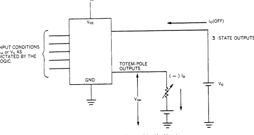
Vee
Vee
•
INPUT CONDITIONS 10l ( + )
V,t-i or V'l AS ....
DICT ATED BY~
1
LOGIC.-1
V,I]
GND VOL
I
I
Figure 148 DC Test Circuit (VIM, VIL, VOL)
I, ( - )
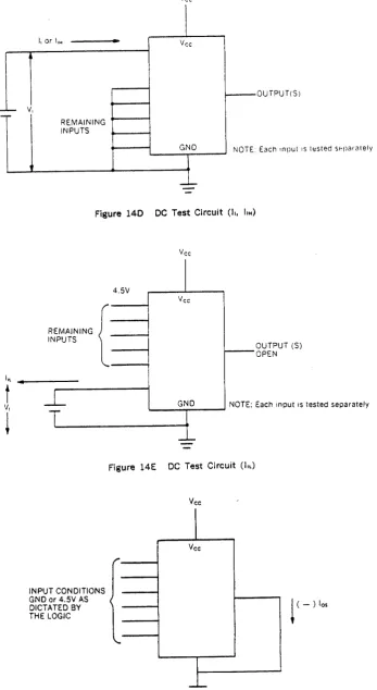
REMAINING INPUTS OPEN
Vee OPEN
Vee
Ol;JTPUT(S) OPEN
L---_ _ --,. _ _ _ ...J NOTE Each Input IS tested separately
Figure 14C DC Test Circuit (VI)
[image:45.611.70.520.32.733.2] [image:45.611.85.508.37.261.2]. - - - -
...--
...
-.~'
-
--,..
I,~
•
t
VI
~
Vee.
I, or I'H
•
Vee•
I - - -OUTPUT(S)
V,
REMAINING INPUTS
GND NOTE: Each Input IS tested sr.-pafCllely
I
l
Figure 140 DC Test Circuit (II. 11M)
4.5V
[
REMAINING INPUTS
INPUT CONDITIONS GND or 4.SV AS DICTATED BY THE LOGIC
Figure 14£ Vee
Vee
OUTPUT (S)
OPEN
GND NOTE: Each Input IS tested separately
DC Test Circuit (IlL)
Vee
Vee
NOTE: Only one output should be shorted at a time. and the duration should not exceed more than a second.
Figure 14F DC Test Circuit (los)
[image:46.611.140.488.61.696.2]Vce
Icc
!
I
INPUT CONDITIONS GND or 4.5 V AS DICTATED BY THE LOGIC
OUTPUT (S) OPEN
GND
1
Figure 14G DC Test Circuit (Icc)
OUTPUT VOLTAGE WAVEFORM IN PHASE
OUTPUT VOLTAGE WAVEFORM OUT OF PHASE
L-H
1SV
lSV
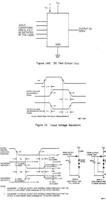
PULSE CONDITIONS FOR DELAY MEASUREMENTS
1 SV
MK-1128
Figure 15 Input Voltage Wavetorm
OUTPUT 3V
~L~~~~1~~L~
...
1 3_V _ _ _ _ _ _ _.If_+~~
____
-ov _ _ _ +-_t_Z_L "'\'~
_ _ ""45VWAVEFORM 1 S1 CLOSEDj--ISEE NOTE 1 I S2 OPEN 1.3V
~
. ,~
_ _ _ _ _ tH"",,\Zt-J:-::~
FROM OUTPUT UNDER TEST
VCC
20011
DIODE FD700
f
ir
'L - - - F V O HWAVEFORM 2 ' \ 5V
(SEE NOTE 21 i~ g~~~ED 1 3V
t ..
1--...:..;;...;;.:;.;;..:;~. - - .. OV S1 AND S2 CLOSED
LOAD e -LOAD CIRCUIT FOR
TTL OUTPUTS
NOTES
WAVEFORM 1 IS FOR AN OUTPUT WITH INTERNAL CONDITIONS SUCH THAT THE OUTPUT IS LOW EXCEPT WHEN DISABLED BY THE OUTPUT CONTROL
WAVEFORM 2 IS FOR AN OUTPUT WITH INTERNAL CONDITIONS SUCH THAT THE OUTPUT IS HIGH EXCEPT WHEN DISABLED BY THE OUTPUT CONTROL
Vee
FROM OUTPUT
{ZOOA
U N D E R m r S T
>
51'O'T
r
f~
y"
I..OAOA-I..OAO el!'!CUIT RlR 3 ·-STATE OUTPUTS
MK-1130
Figure 16 Outputs Voltage Waveto'rms (3-State)
40
[image:47.611.135.479.69.712.2]- - - -_ _ _ _ _ _ _ _ _ _ _ _ _ _ . - . ' ... ,"-""~I.' ~~,
10lF
20/F
S·A
RO
LO
CLK.C+-_ _ _ --f--.:._---'
CLK.A+-_ _ _ _ _
+-____
-+-+-____ ~RO.A~----r---__ ~~~~---~~--~
[image:48.613.155.468.164.415.2]CLEAR LOAO MK·1143
Figure 17 De006 Timing Diagram
Table 6 Setup Time and Pulse Width Switching Characteristics·
Time Description Signal Min
t3 Pulse width (min) S-C to SeA 50 ns
t5 Setup time DfF (7:0) to LD 10 ns
t6 Setup time S-C to LD 10 ns
t7 Pulse width (min) LD 90 ns
t8 Setup time S-C to RD 20 ns
tIl Clock pulse width (min) ClK-C (HI) 40 ns
t14 Setup time S-C to SeA 20 ns
t15 Setup time SeA to RD 10 ns
t16 Clock pulse width (min) ClK-A (HI) 40 ns
t18 Setup time CNT1 A to ClK-A 45 ns
t21 Setup time RD to RD-A 15 ns
t24 Clock off time (min) ClK-A. ClK-C 40 ns t25 Data hold time lD to DATA IN 20 ns
Table 7 Switching Characteristics·
Propagation
Input Signal Output Signal Test Delay (ns)
Time Name Polarity Name Polarity Conditions Min Max
t, S-C H-L OfF (7:0) X-L Load A 15 80
S-A H-L RD-A= O.4V
(C Counter)
t2 S-C H-L OfF (7:0) X-L Load A 15 80
S-A H-L AD-A= O.4V
(A Counter)
t4 AD L-H OfF (7:0) OfF (7:0)-Z Load A 10 30
t9 AD H-L OfF (7:0) Z-OfF (7:0) Load A 34 80 ~
t,o CLK-C H-L OfF 1 L-H Load A 18 55
t 12, CLK-C L-H MAX-C L-H Load B 10 35
t'9 CLK-A MAX-A
t'3 CLK-C H-L MAX-C H-L Load B 10 35
t17 CLK-A H-L OfF 2 L-H Load A 18 55
t20 CLK-A H-L MAX-A H-L Load B 10 35
t22 RO-A L-H OfF (7:0) Z-L Load A 10 30
Z-H Load A 10 30
t23 AD-A H-L OfF (7:0) L-Z Load A 8 25
H-Z Load A
8
25• Loads are presented in Figure 16.
Vee
=
5.0 ::: 0.25 V42
- - - , , - _ .
_.-DC010 DIRECTMEMORY ACCESS LOGIC{DEC # 19-14038-00)
The direct memory access (DMA) chip is a 20'pin, 0.762 cm center X 2.74 cm long (0.3 in center, X 1.08 in long) DIP, low-power Schottky device for primary use in DMA peripheral device interlaces using the LSI·II bus.
This device provides the logic to perlorm the handshaking operations required to request and to gain control of the system bus. Once bus mastership has been established, the DC010 generates the required sig· nals to perlorm a DATI, DATa, or DATIO transfer as specified by control lines to the chip. The OCala IC has a control line that will allow multiple transfers or only four transfers to take place before giving up bus master· ship.
Figure 18 is a simplified logic diagram of the DC010 IC. The logic symbols and truth table are presented in Figure 19 and the DCOIO volt· age waveforms are shown in Figure 21. Table 8 describes the signals and pins of the OCala by pin and Signal name. Figures 22 through 26 show the timing for the OCala while the setup time and pulse width specifications are listed in Table 9. The switching characteristics are presented in Table 10. Figure 20 shows the various test conditions em-ployed to derive the data presented in the Electrical Characteristic. (MASTIR S'O HI _ _ _ _
-q---,
Ala H - - - 1
(A .... V S'O HI _ _ _ _ _ _ .q
IN.T
t.--..I--i---'-it==::j::==---t+::=_-=====:::;"']
CNT4 H
____
+-_-;---.
IMASTliR
ENAHI
'MOUT
H...:=--+I::if---+-L;o---h
OArtN ~.,.---_q---.,.
t;:::============='SYHC H
OArtO ~---"""'---"=""-CI
(ENO CYCLE HI
IIN.T H'
elK L
IMASTliR ENA
ASYNC H
HI==t:========a~lEND 1 I - - + : : = = = = = = = = = = = = = ± = = = - _ - - . J
Figure 18 DC010 Simplified Logic Diagram
TRUTH TABLE WHERE l " TTL WW
H • TTL HIGH X • DONT CARE
INPUTS DATI III DAno
x L L H
H H
TRANSFER TYPE
DATIO
DAf! DArO
Figure 19 DC010 Logic Symbol/Truth Table
43
.;;>----+-MASTER H
MK·1141
[image:50.611.157.497.269.535.2]Pin 1
13
16
14
3
2
Table 8 DC010 Pin/Signal Descriptions Signal
REQ H
BDMGI L
CNl4 H
TMOUT H
DATIN L
DATIO L
Description
*
Request (TTL Input). A high on this signal init-iates the bus request transaction. A low allows the termination of bus mastership to take place. DMA Grant Input (Hi-Z Input). A low on this signal allows bus mastership to be established if a bus r&>quest was pending (REQ
==
high); otherwiSe this signal is delayed and output as 8DMGO L.Count Four Input (TTL Input). A high on this signal allows a maximum of four transfers to take place before giving up bus mastership. A low disables this feature and an unlimited trans-fer will take place as long as REQ is higi1. If left open, this pin will assume a high state.
Time-Out (TTL Input/Open Collector Output). This I/O pin is low while MASTER ENA is high. It goes into high impedence when MASTER ENA is low. When driven low it prevents the assertion of BDMR; when driven high it allows the asser· tion of BDMR to take place if BDMR has been negated due to the 4·maximum transfer condi· tion. An RC network may be used on this pin to delay the assertion of BDMR.
Data In (TTL Input). This signal allows the selec-tion of the type of transfers to take place~ accord· ing to the truth table (Figure 19).
Data In/Out (TTL Input). This signal allows the selection of the type of transfer to ta.le place according to the truth table (Figure 19' During a DATIO transfer, this signal must be l'.,ggled in order to allow the completion of the out~ut por· tion of the I/O transfer.
If left open, this pin will assume a high state. • Refer to Figures 22 through 26.
44
"~IIiIIII _ _ IIUII.liI =:_1111 _ _ •••• ' . . 4I11III: : _ · " - - - " -_ _ •• "_IIIIIIIIIIII' •• __
IIlI' ... ---_:_.I ______ ... ______
.:Ii ____
•• "
....
,.::.$1_41_1111
[image:51.614.169.483.231.604.2]