N A N O E X P R E S S
Open Access
Band Offset Measurements in
Atomic-Layer-Deposited Al
2
O
3
/Zn
0.8
Al
0.2
O
Heterojunction Studied by X-ray
Photoelectron Spectroscopy
Baojun Yan
1*, Shulin Liu
1, Yuekun Heng
1, Yuzhen Yang
1,2, Yang Yu
1,3and Kaile Wen
1,4Abstract
Pure aluminum oxide (Al2O3) and zinc aluminum oxide (ZnxAl1-xO) thin films were deposited by atomic layer deposition (ALD). The microstructure and optical band gaps (Eg) of the ZnxAl1-xO (0.2≤x≤1) films were studied by X-ray diffractometer and Tauc method. The band offsets and alignment of atomic-layer-deposited Al2O3/Zn0.8Al0.2O heterojunction were investigated in detail using charge-corrected X-ray photoelectron spectroscopy. In this work, different methodologies were adopted to recover the actual position of the core levels in insulator materials which were easily affected by differential charging phenomena. Valence band offset (ΔEV) and conduction band offset (ΔEC) for the interface of the Al2O3/Zn0.8Al0.2O heterojunction have been constructed. An accurate value ofΔEV= 0. 82 ± 0.12 eV was obtained from various combinations of core levels of heterojunction with varied Al2O3thickness. Given the experimentalEgof 6.8 eV for Al2O3and 5.29 eV for Zn0.8Al0.2O, a type-I heterojunction with aΔECof 0.69 ± 0.12 eV was found. The precise determination of the band alignment of Al2O3/Zn0.8Al0.2O heterojunction is of particular importance for gaining insight to the design of various electronic devices based on such heterointerface.
Keywords:Atomic layer deposition, X-ray photoelectron spectroscopy, Heterojunction, Microchannel plate
Background
Nano-thick oxide films with high resistance have attracted much attention as the most promising conductive layer for the applications of microchannel plate (MCP) as elec-tron multiplier [1, 2], resistive memories [3], and elecelec-tron- electron-optical micro-electro mechanical systems (MEMS) [4]. A large research effort has been devoted to the novel idea of adjusting resistivity of such thin films due to the above-mentioned large potential applications in a special envir-onment. MCP is a thin glass plate with thickness of about 500μm consisting of several millions pores of a cylinder geometry with a 4–25-μm diameter and with a bias angle usually 5°–13° to the normal of the plate surface, and the high aspect ratio in each pore is about 20:1–100:1 [5, 6]. For recent MCP fabrication, two kinds of nano-thick
layers are deposited on the MCP pore surfaces to conduct an electron multiplication function [1, 2]. The first layer is a conductive layer for supplying electrons, and the second layer is a secondary electron emission (SEE) layer for generating electrons. The three-dimensional surfaces and high aspect ratio of MCP should be firstly taken into consideration for depositing uniform thickness and composition of thin films. So far, the only effective approach growing high-quality thin films is the atomic layer deposition (ALD) technique based on sequential self-terminating gas-solid reactions [7].
ZnO is an n-type semiconductor with a direct bandgap of around 3.37 eV and a large exciton binding energy of 60 meV at room temperature [8, 9]. A lot of elements such as Mg [10, 11], Cd [12], Ga [13], W [14], and Mo [15] were used to doping in ZnO in order to tune its optical and electrical properties for special applications. In electron multiplier application, such as MCP, zinc aluminum oxide (ZnxAl1-xO) films have been
investi-gated because of their thermal stability in a special
* Correspondence:yanbj@ihep.ac.cn
1State Key Laboratory of Particle Detection and Electronics, Institute of High
Energy Physics of Chinese Academy of Sciences, Beijing 100049, People’s Republic of China
Full list of author information is available at the end of the article
application environment and low cost of industrialization. The properties of ZnxAl1-xO films can be controlled by
changing the Al content, paving a way to design optoelec-tronic and photonic devices based on this material. Usu-ally, high-resistivity ZnxAl1-xO thin films as a conductive
layer withxat the range of 0.7–0.85 have been applied in the field of electron multiplier [16]. For SEE layers, boron-doped diamond with hydrogen-terminated material has higher SEE coefficient than that of other traditional insula-tors. This provides a strong impetus for the development of electron multipliers. However, in the presence of degradation due to electron beam-induced contamin-ation, these must be seriously regarded as preliminary [17]. From a practical point of view, two kinds of traditional insulators used as SEE layers in MCP are magnesium oxide (MgO) and Al2O3 thin films [18].
Although pure MgO has higher SEE coefficient than that of Al2O3, it is limited in the application on MCP
because it is highly deliquescent and its surface is ra-ther reactive with atmospheric moisture and carbon dioxide as demonstrated by our previous work [19], which probably results in degraded SEE performance. However, the physical and chemical properties of Al2O3are
very stable even after long-term exposure to the atmos-phere. Therefore, Al2O3is one of the most commonly used
SEE materials in MCP application.
According to the structure of MCP, the Al2O3 and
ZnxAl1-xO thin films have different band gaps (Eg)
result-ing in band offsets in the heterointerface. Therefore, the determination of the band offsets at Al2O3/ZnxAl1-xO
interface is of importance because valence band offset (ΔEV) and conduction band offset (ΔEC) can deteriorate
or promote SEE performance and also have a great influ-ence on the performance of electron multiplier.
Generally, Kraut’s method is widely used to calculate the valence band maximum (VBM) and the conduction band minimum (CBM) of semiconductor/semiconductor heterojunctions [20]. However, in the case of insulator/ semiconductor or, in more serious cases, insulator/insu-lator heterojunctions, the positive charges generated during X-ray bombardment accumulate in the insulators and induce a strong modification of the kinetic energy of the emitted photoelectrons which is the so-called dif-ferential charging effect [21]. Although it is probably dealt with using a neutralizing electron gun [22], the use of C 1s peak recalibration [23], and zero charging method [24–26], a careful evaluation of the experimental result is necessary due to the differential charging effect during X-ray irradiation [19].
In this work, we will study the structure and opticalEg
of ZnxAl1-xO (0.2≤x≤1) thin films firstly, and then, we
especially determine the ΔEV and ΔEC of the Al2O3/
Zn0.8Al0.2O heterojunction by using high-resolution
X-ray photoelectron spectroscopy (XPS).
Methods
Sample Preparation
Several samples were used in this study: nine 80-nm-thick ZnxAl1-xO samples (0.2≤x≤1) individually grown
on n-Si (1 1 1) and quartz substrates, a 30-nm-thick Al2O3grown on n-Si (1 1 1) substrate, and 3, 4, 5, 8 nm
of Al2O3on 80 nm of Zn0.8Al0.2O grown on n-Si (1 1 1).
The quartz substrates were ultrasonically cleaned in an ethanol/acetone solution and then rinsed in deionized water. The polished Si substrates were dipped in hydro-fluoric acid for 30 s and then placed in an ALD chamber waiting for deposition. For ZnxAl1-xO layer deposition,
ZnO:Al2O3ALD was carried out using diethylzinc (DEZ),
trimethylaluminum (TMA), and deionized water as Zn, Al, and oxidant precursor, respectively. The Al2O3 ALD
was performed using separate TMA and H2O exposures
with sequence TMA/N2/H2O/N2 (150 ms/4 s/150 ms/
4 s). The ZnO ALD was performed using separate DEZ and H2O exposures following the sequence DEZ/N2/H2O/
N2(150 ms/4 s/150 ms/4 s). The doping was carried out
by substituting TMA exposure for DEZ. The Zn contents in the ZnxAl1-xO layers were controlled by adjusting the
ratio of the pulse cycles of DEZ and TMA, where the Zn content x was varied from 0.2 to 1 (pure ZnO) atom %. For Zn0.8Al0.2O layer, the DEZ and H2O
pulses were alternated, and every fifth DEZ pulse was substituted with a TMA pulse. Ultrahigh purity nitro-gen was used as a carrier and purge gas. The reaction temperatures were 200 °C. The detailed parameters are listed in Table 1.
Characterization
Optical transmittance spectra in a wavelength range from 185 to 700 nm were carried out by using a double-beam UV-Vis-IR spectrophotometer (Agilent Cary 5000) at room temperature in air. The crystal structure of the films were characterized by X-ray diffraction (XRD, Bruker D8) using Cu Kα radiation (40 kV, 40 mA, λ=
Calculations
TheΔEVof the Al2O3/Zn0.8Al0.2O heterojunction can be
calculated from Kraut’s formula
ΔEV¼ EZn0CL:8Al0:2Oð Þy−EZn0VBM:8Al0:2O
‐ EAl2O3
CL ð Þx−EAl2O3VBM
‐ΔECL
ð1Þ
where ΔECL¼ ECLZn0:8Al0:2Oð Þy −E Al2O3
CL ð Þx
was the energy
difference between feature y and feature x CLs, which were measured by XPS measurement in the heterojunc-tion sample, and EAl2O3
CL ð Þx −E Al2O3
VBM
and EZn0:8Al0:2O
CL ð Þy −
EZn0:8Al0:2O
VBM Þ were the Al2O3 and Zn0.8Al0.2O bulk
con-stants, which were obtained on the respective thick films. The VBM values were determined by linear ex-trapolation of the leading edge to the baseline of the valence band spectra. A root sum square relationship is used to combine the uncertainties in the different binding energies to determine the uncertainty of cal-culated results [26].
Results and Discussion
Structure and Band Gaps of ZnxAl1-xO Samples
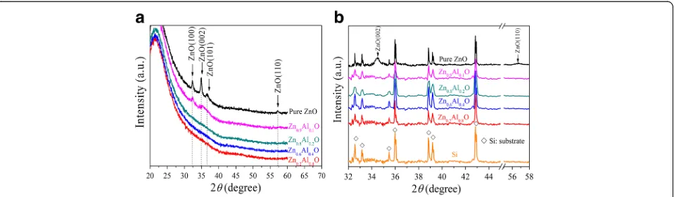
The XRD patterns of the as-deposited 80-nm-thick ZnxAl1-xO (x= 0.2, 0.6, 0.8, 0.9, 1) thin films grown on
quartz and Si substrates are shown in Fig. 1a, b, respect-ively. For the pure ZnO grown on quartz substrates in Fig. 1a, the strong peaks at 32.4° and 34.8° and the
relatively weak peaks at 36.5° and 57.2° come from hexagonal ZnO phase, indicating the polycrystalline na-ture of the ZnO layer. And strong (0 0 2) peak shows the preferential orientation growth of ALD ZnO. How-ever, the above characteristic peaks become weak for Zn0.9Al0.1O sample and disappear for ZnxAl1-xO (x≤0.8)
samples, which suggests that ZnO crystallization is suppressed with Al concentration increase. Besides, the broad peak ranging from 20° to 30° is the typical pattern of the quartz substrate. For Si substrate, the strong peaks around 28.4° and 58.9° are easily detected (data not shown). These peaks are corresponding to the diffrac-tions originated from Si (1 1 1) and Si (2 2 2) crystal planes. In addition, the relatively weak peaks in Fig. 1b at 2θ= 32.6°, 33.2°, 35.4°, 35.9°, 38.8°, 39.2°, and 42.8° in the diffractograms that arise from the Si substrate itself are also observed. These unknown peaks may be related to the process conditions for producing crystalline sili-con and are observed in previous work [27, 28]. Except for diffraction peaks from the Si substrate, no other diffraction peaks from the ZnxAl1-xO (x≤0.9) samples
are detected. Only (0 0 2) and weak (1 1 0) peaks appear in the pure ZnO sample. From the above results, the crystal quality of the ZnxAl1-xO film is a serious decline
[image:3.595.55.539.99.196.2]with the increasing concentration of Al content. It is well known that the particle size of Al ions is less than that of Zn ions. Zn is easily substituted by Al when dop-ing concentration of Al increases. This results in weak-ened ZnO crystallinity, so the structure of ZnxAl1-xO Table 1Detailed parameters for Zn0.8Al0.2O and Al2O3layers
Sample no. Substrate Material Thickness (nm) Composition Characterization
ALD01 n-Si (111), quartz Zn0.8Al0.2O 80 Zn:Al = 4:1 (atomic ratio) XPS, XRD and UV-Vis
ALD02 n-Si (111) Al2O3 30 Pure XPS
ALD03 n-Si/ALD01 Al2O3 3 Pure XPS, SE
ALD04 n-Si/ALD01 Al2O3 4 Pure XPS, SE
ALD05 n-Si/ALD01 Al2O3 5 Pure XPS, SE
ALD06 n-Si/ALD01 Al2O3 8 Pure XPS, SE
[image:3.595.60.539.574.714.2](x≤0.8) samples is amorphous, in good agreement with previous results [29]. Taken into consideration, ZnxAl1-xO
layer growth appears to be substrate sensitive and Al dop-ing concentration has an influence on the crystallization of the films.
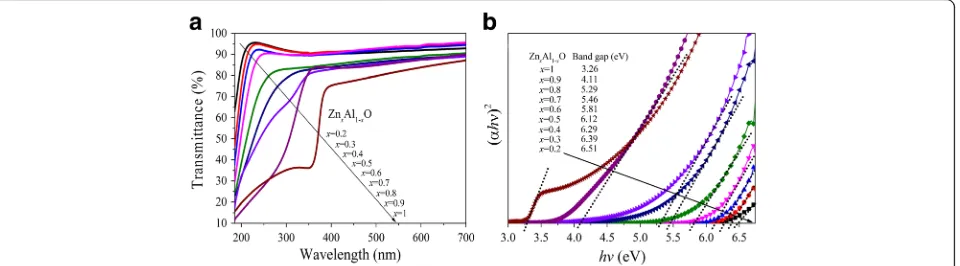
Figure 2a shows transmission spectra of the ZnxAl1-xO
samples deposited on quartz substrate. The average transmittance is above 80% in the visible wavelength for all samples. It is found that ZnO film exhibits abrupt absorption edge which appears at ~390 nm correspond-ing to the fundamental Eg of ZnO. A blue shift of the
absorption edge is apparently observed when Al concen-tration increases. TheEg of ZnxAl1-xO thin films can be
obtained by fitting the sharp absorption edges. The rela-tionship between absorption coefficient (α) and Eg of
direct band gap semiconductor is given by Tauc equa-tion [30], (αhv)2= B(hv−Eg), where hν is the photon
energy and B is a constant. The dependence of (αhν)2on photon energy is shown in Fig. 2b. TheEgis obtained by
the extrapolations of the liner regions of the optical ab-sorption edges. The Egof pure ZnO thin film deposited
by ALD is 3.26 eV, which is consistent with the previous reports [31, 32]. With the Zn concentrationx decreases from 0.9 to 0.2, theEgof ZnxAl1-xO thin films increases
from 4.11 to 6.51 eV. It is directly demonstrated that the
Eg of ZnxAl1-xO thin films can be adjusted in a large
range by controlling the Al doping concentration, which makes it a suitable candidate for application in many scientific research fields [33, 34]. For the new type of MCP, the properties of Zn0.8Al0.2O thin film are suitable
for conductive layer proved by previous study [2]. There-fore, the Eg of atomic-layer-deposited Zn0.8Al0.2O thin
film is 5.29 eV, which is sufficient to make a band gap discontinuity in Al2O3/Zn0.8Al0.2O heterojunction and is
used for calculating theΔECvalue later.
Valence and Conduction Band Offset Measurements of Al2O3/Zn0.8Al0.2O Heterojunction
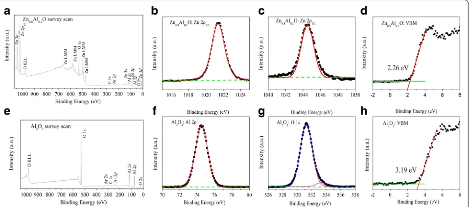
The XPS spectra of survey scan, CLs, and VBM region for Zn0.8Al0.2O and Al2O3samples are shown in Fig. 3.
In this study, we find that the CLs positions of the Zn0.8Al0.2O and Al2O3 thin films do not change as a
function of X-ray irradiation time for 15 min (data not shown), because of operating a low energy electron flood gun. Figure 3a, e shows the whole scanning spectrum of the thick Zn0.8Al0.2O and Al2O3thin films, respectively.
The C 1speak at 284.6 eV appeared due to some surface contamination, and the Ar 2ppeak at 242.1 eV appeared because of residual inert gas composition in the ultra-high vacuum chamber. The peaks in Fig. 3a located 660, 652, 582, 573, 559, 495, and 472 eV are Auger lines of Zn element. The stoichiometry of the thick films are checked by the ratio of the integrated area of Zn 2ppeak to Al 2ppeak for the Zn0.8Al0.2O sample and Al 2ppeak
to O 1s peak for the Al2O3sample. Both are corrected
by corresponding atomic sensitivity factorsS[35], taking into account their corresponding photoionization cross-sections of CLs calculated by Scofield [36], and the mean free path of the photoelectrons calculated by Tanuma et al [37]. Here, the S values are calculated to be 0.256, 2.768, and 0.733 for Al 2p, Zn 2p3/2, and O 1s. The
atomic ratios Zn:Al = 3.97:1.01 for Zn0.8Al0.2O and
Al:O = 1.99:3.01 for Al2O3compare well with that of
de-signed ratio of atomic layer deposition, which indicate good stoichiometry of the Zn0.8Al0.2O and Al2O3 layers.
The high-resolution scans of Zn 2p3/2and Zn 2p1/2CLs of
Zn0.8Al0.2O are shown in Fig. 3b, c. The peaks fitted using
Shirley backgrounds and Voigt (mixed Lorentzian-Gaussian) functions located 1021.41 and 1044.51 eV in Fig. 3b, c correspond to the electronic states of Zn 2p3/2
and Zn 2p1/2, respectively, and both are fitted by a single
contribution, attributed to the bonding configuration Zn-O. The Al 2ppeak of Al2O3located 74.35 eV and O 1s
peak located 531.1 eV are shown in Fig. 3f, g. The Al 2p spectrum as fitted by a single contribution, attributed to the bonding configuration Al-O. However, for the O 1s spectrum, an additional peak low-intensity higher binding energy component is also observed. This extra component is attributed to both O-Al and O-H bonds [38]. The VBM positions are determined by a linear extrapolation of the
Fig. 2Transmittance spectra (a) and the plots of (αhν)2vs. photon energy (b) of Zn
[image:4.595.61.541.580.713.2]leading edge of the valence band spectrum and the back-ground [39], as shown in Fig. 3d,h. This linear method has already been widely used to determine the VBM of semi-conductors with high accuracy. The VBM values of atomic-layer-deposited thick Zn0.8Al0.2O and Al2O3
samples are 2.26 and 3.19 eV, respectively. The scatter of the data relative to the fit are estimated as an un-certainty in VBM positions of less than 0.03 eV. The parameters deduced from Fig. 3 are summarized in Table 2 for clarity.
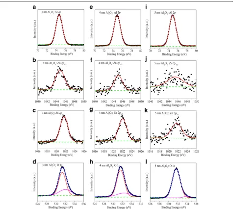
Four CLs of Al2O3/Zn0.8Al0.2O heterojunction with
different Al2O3thickness are shown in Fig. 4. The Al 2p,
Zn 2p1/2, and Zn 2p3/2XPS spectra in Fig. 4(a, e, i), (b, f, j),
and (c, g, k), respectively, are fitted by a single contribution, attributed to the bonding configurations Al-O and Zn-O. For the O 1s XPS spectrum in Fig. 4d, h, l, an additional low-intensity higher binding energy compo-nent is observed. The extra compocompo-nent is attributed to metal (Al, Zn)-O bonding at the interface and/or inelastic losses to free carries in the Al2O3layer, similar
results obtained by previous study [19]. With the increase of the Al2O3 thickness, the intensity of Zn 2p1/2 peak is
weakened while the energy resolution is deteriorated shown in Fig. 4f. It is difficult to observe and fit for Al2O3
thickness of 5 nm as shown in Fig. 4j. So, the peak position of Zn 2p1/2in 5-nm Al2O3sample listed by a bold
number in Table 2 is a large deviation as a result of the big error of fitting. The CLs of Al2O3/Zn0.8Al0.2O samples
are summarized in Table 2.
The ΔEV of the Al2O3/Zn0.8Al0.2O heterojunction is
determined from the energy separation between the CLs in the Al2O3/Zn0.8Al0.2O sample and the VBM to CLs
separations in the thick Al2O3and Zn0.8Al0.2O samples,
respectively. Table 3 lists the ΔEVvalues for all Al2O3
samples with thickness of 3–5 nm, and the error in each value is ± 0.07 eV. Therefore, the averaged ΔEVvalue is
0.87 ± 0.22 eV. It is important to note that the cal-culation does not include the italic numbers in Table 3 because of the big error fitting of CLs of Zn 2p1/2in the
5-nm Al2O3/Zn0.8Al0.2O sample.
However, there are obvious considerable CL shifts up to 0.6 eV sensitive to the thicknesses of the Al2O3and
Zn0.8Al0.2O layers from the given experimental data in
Table 2, and different ΔEV values are obtained in the
Fig. 3XPS spectra forasurvey scan,bZn 2p3/2,cZn 2p1/2, anddVBM of Zn0.8Al0.2O andesurvey scan,fAl 2p,gO 1s, andhVBM of Al2O3, with
[image:5.595.60.539.89.301.2]application of a low-energy electron flood gun
Table 2Peak positions of CLs and VBM positions used to calculate theΔEVof the Al2O3/Zn0.8Al0.2O heterojunction
Zn0.8Al0.2O Al2O3 3 nm Al2O3/Zn0.8Al0.2O 4 nm Al2O3/Zn0.8Al0.2O 5 nm Al2O3/Zn0.8Al0.2O
Al 2p 74.35 74.6 74.93 74.87
O 1s 531.1 531.32 531.66 531.63
Zn 2p3/2 1021.41 1021.69 1022.05 1021.97
Zn 2p1/2 1044.51 1044.85 1045.11 1045.64
VBM 2.26 3.19
[image:5.595.56.541.639.724.2]various combinations of XPS CLs in Table 3. It is dir-ectly proved that the charging phenomenon generated by the X-ray irradiation results in adverse effects on the
ΔEV determination when taking XPS measurement on
insulator/semiconductor heterojunction in spite of oper-ating neutralizing electron gun. As has been widely reported, the influences of differential charging on the
band offsets determination cannot be neglected even in very thin oxides. Therefore, zero charging method is adopted in this study in order to eliminate charging-induced errors and recover the accurateΔEVvalue.
The error in the ΔEV measurement is resulting from
the differential charging effect that prevents the correct determination of the energy differences, such as between
Fig. 4CLs of Al2O3/Zn0.8Al0.2O samples with varied Al2O3thicknessa–d3 nm,e–h4 nm, and i–l5 nm, with application of a low-energy
[image:6.595.61.537.86.512.2]electron flood gun
Table 3TheΔEVvalues of the Al2O3/Zn0.8Al0.2O heterojunction with Al2O3thickness of 3–5 nm
ΔEV 3 nm Al2O3/Zn0.8Al0.2O 4 nm Al2O3/Zn0.8Al0.2O 5 nm Al2O3/Zn0.8Al0.2O
Zn 2p3/2 Zn 2p1/2 Zn 2p3/2 Zn 2p1/2 Zn 2p3/2 Zn 2p1/2
Al 2p 0.9 0.84 0.87 0.91 0.89 0.32
O 1s 0.87 0.81 0.85 0.89 0.9 0.33
[image:6.595.56.542.669.726.2]the Al 2pand Zn 2p3/2 signals even in very thin Al2O3
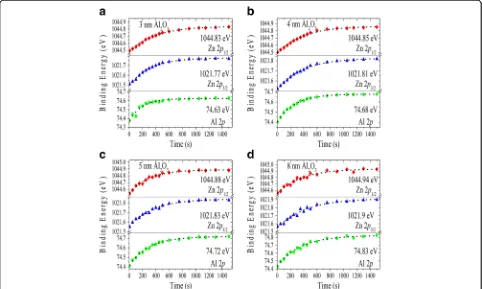
films in heterojunction. In Fig. 5, the binding energies of the Al 2p, Zn 2p3/2, and Zn 2p1/2CLs for the 3, 4, 5, and
8 nm Al2O3 films are plotted as a function of X-ray
irradiation time. The binding energies of Al 2p, Zn 2p3/2,
and Zn 2p1/2 CLs of the 3-nm Al2O3 sample in Fig. 5a
increase slowly until they stabilize on a steady state value of 74.63 ± 0.01, 1021.77 ± 0.01, and 1044.83 ± 0.02 eV, respectively. Similar time dependencies are observed in the 4-, 5-, and 8-nm Al2O3films, as shown in Fig. 5b–d.
The results show that CL steady state spectra are obtained after stabilization of the signals in the heterojunction-considered charge saturated when X-ray irradiation time is more than 25 min. Therefore, X-ray irradiation time is one of the most important parameters to determine the insulator/semiconductor band offsets. Layer thickness de-pendence in peak positions is mainly resulting from the differential charging effects. True peak positions can be acquired by extrapolating the measured binding energies to zero oxide thickness and ideally to zero charge, similar results are reported for SiO2/Si [25], HfO2/Si [26], and
MgO/Zn0.8Al0.2O [19] systems.
The CLs positions of the Al 2p, Zn 2p1/2, and Zn 2p3/2
are plotted as a function of the Al2O3 film thickness,
as shown in Fig. 6. By linear fitting of the experimen-tal data, the CLs positions of the Al 2p, Zn 2p1/2, and
Zn 2p3/2 peaks are determined to be 74.51 ± 0.03,
1044.77 ± 0.06, and 1021.7 ± 0.04 eV, respectively. In order to correct the ΔEV of the Al2O3/Zn0.8Al0.2O
heterojunc-tion, we calculate the energy differences between the extrapolated (Al 2p, Zn 2p1/2) and (Al 2p, Zn 2p3/2)
at zero thickness. The values are 970.26 ± 0.07 and 947.19 ± 0.05 eV, respectively. Inserting these values in Eq. (1), the ΔEV are calculated to be 0.83 ± 0.09 and
0.8 ± 0.08 eV, which is in good agreement using the two combinations of CLs of the Al2O3/Zn0.8Al0.2O
heterojunction. Therefore, the averaged ΔEV value is
0.82 ± 0.12 eV.
There are three possible reasons that affect the ΔEV
values in addition to the XPS method itself. Firstly, the oxide stoichiometry of the Al2O3thin films measured by
XPS is almost the same in the different Al2O3samples
with thickness of 3–8 nm. Therefore, the composition of the Al2O3film is independent of thickness and the
bind-ing energy shifts in Fig. 5 is related to the differential charging effect occurring in the Al2O3/Zn0.8Al0.2O
het-erojunction during X-ray irradiation. Secondly, band bending at the heterointerface could induce a systematic error in determination of ΔEV, and we check that this
error is much smaller than the average standard devi-ation of ± 0.03 eV given above. Finally, the strain existing in the Al2O3overlayer of the heterojunction will induce
Fig. 5Time-resolved plots showing the respective binding energies vs. X-ray irradiation time fora3 nm,b4 nm,c5 nm, andd8 nm Al2O3films
[image:7.595.57.539.412.701.2]a piezoelectric field that probably affects the measured
ΔEV value, a similar phenomenon explained by Martin
et al [40]. The heterojunction underlayer Zn0.8Al0.2O is
thick enough, and the structure of both materials is amorphous. Therefore, the strain-induced piezoelectric field is not taken into consideration in this study.
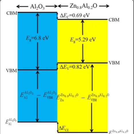
To infer the ΔEC based on the value ofΔEV, we need
to know theEgof the ultrathin Al2O3layer, which can be
estimated from O 1s core-level binding energy spectrum of atomic-layer-deposited Al2O3 thin films with energy
loss structure. The binding energy is calculated from the difference in the total photoelectron energy minus the kinetic energy due to the loss in photoelectron energy by inelastic collision processes within the sam-ple. The minimum inelastic loss is equal to the band gap energy, and the most cited value of Eg is 6.8 eV
[41–43]. Together with the Zn0.8Al0.2O Eg of 5.29 eV
at room temperature, theΔECcan be simply derived by the
equation, ΔEC=Eg(Al2O3)−ΔEV−Eg(Zn0.8Al0.2O), where
Eg(Al2O3) and Eg(Zn0.8Al0.2O) are the band gaps of the
Al2O3and Zn0.8Al0.2O thin films, respectively. TheΔEC is
calculated to be 0.69 ± 0.12 eV, which means that the barrier height for transport of electrons is smaller than that of holes. The band alignment of the Al2O3/Zn0.8Al0.2O
heterojunction obtained from XPS measurements is shown in Fig. 7. The CBM of Al2O3 is higher than that of
Zn0.8Al0.2O; however, the VBM of Al2O3is lower than that
of Zn0.8Al0.2O. Therefore, a nested type-I band alignment
with a ratioΔEC/ΔEVof about 1:1.2 is obtained.
Usually, the MCP gain under direct current (DC) mode is limited by the space charge density without consideration of ion feedback, and the recharge time constant or dead time (τ) is several milliseconds [44]. When operating a MCP as a DC current amplifier, the gain is constant until the output current (Ioc) exceeds
about 10% of the strip current through the plate. How-ever, the MCP works in a highly saturated state under a photon-counting mode, and the electron avalanche multiplication is done within several nanoseconds that is a million times faster than τ [44–46]. The peak output
current in pulsed operation exceeding theIocby several
orders of magnitude is observed. Therefore, anode signal charges probably come from the tunneling electrons in the Al2O3/ZnxAl1-xO heterojunction of the inner wall of
the MCP. For photon-counting mode, both ΔEV and ΔEC should be sufficiently large, which can prevent the
thermal excitation of electrons generated from the SEE layer into the electron multiplier system that probably produces high electronics dark noise and result in a reduced signal to noise ratio. The present result has no effects on the MCP operating under DC mode which is determined by space charge saturation, but has negative effects on the photon-counting mode which needs a type-II heterojunction to improve tunneling probability for excellent performance. The relationship between the Al2O3/ZnxAl1-xO heterojunction and charge replenishment
Fig. 6Al 2p(a), Zn 2p1/2(b), and Zn 2p3/2(c), CL binding energies as a function of the Al2O3thin film thickness
Fig. 7The schematic diagram of band offset at the Al2O3/Zn0.8Al0.2O
[image:8.595.56.542.88.226.2] [image:8.595.305.539.467.699.2]mechanism under photon-counting mode needs further study. Therefore, the band alignment of the Al2O3/
ZnxAl1-xO heterojunction should be constructed and
adjusted by appropriately changing the ratio of Al and Zn elements under the premise of meeting the require-ments of the electron multiplier.
Conclusions
The structure and optical band gaps of ZnxAl1-xO
(0.2≤x≤1) films deposited by atomic layer deposition are investigated. And the band offset measurements of the Al2O3/Zn0.8Al0.2O heterojunction have been
determined by XPS with zero charging method. The results show that X-ray irradiation time is one of the most important parameters to determine the band offsets. The layer thickness dependence in peak positions is mainly derived from the differential charging effects, and true peak positions are obtained by extrapolating the measured binding energies to zero oxide thickness and ideally to zero charge. The ΔEVvalue is obtained to be
0.82 ± 0.12 eV, and the correspondingΔECis calculated to
be 0.69 ± 0.12 eV. Therefore, a nested type-I band align-ment is obtained. Understanding of the band alignalign-ment parameters of the Al2O3/Zn0.8Al0.2O interface will
facili-tate the knowledge of their carrier transport mechanism and design of corresponding hybrid devices, especially in the research process of electron multipliers.
Abbreviations
Al2O3:Aluminum oxide; ALD: Atomic layer deposition; CBM: Conduction
band minimum; CLs: Core levels; DC: Direct current; DEZ: Diethylzinc;
Eg: Band gap;Ioc: Output current; MCP: Microchannel plate; MgO: Magnesium
oxide; SEE: Secondary electron emission; TMA: Trimethylaluminum; VBM: Valence band maximum; XPS: X-ray photoelectron spectroscopy; XRD: X-ray diffractometer; ZnxAl1-xO: Zinc aluminum oxide;ΔEC: Conduction
band offset;ΔEV: Valence band offset
Acknowledgements
We express our sincere gratitude to the reviewer, who has given us the most valuable advice. We thank Dr. Lin Wang and Dr. Hailiang Nie for the meaningful discussions on XRD measurement and chemical formula of Zn0.8Al0.2O, respectively. We are especially grateful to Danjiao Wang for her
careful reading and polishing the manuscript.
Funding
This work was supported by the National Natural Science Foundation of China (Nos. 11675278 and 11535014), the Strategic Priority Research Program of the Chinese Academy of Sciences (No. XDA10010400), and the Beijing Municipal Science and Technology Project (No. Z171100002817004).
Availability of Data and Materials
The raw data used in this study is not available for the time being, because the data has not been fully analyzed, and the results of the analysis will be gradually introduced in the recent published articles.
Authors’Contributions
BY designed and conducted the experiments and drafted the manuscript. YY, YY and KW prepared the thin films and performed the XRD, UV-Vis-IR and XPS measurements. SL and YH provided the technical support and ad-vices on the work. All authors read and approved the final manuscript.
Competing Interests
The authors declare that they have no competing interests.
Publisher’s Note
Springer Nature remains neutral with regard to jurisdictional claims in published maps and institutional affiliations.
Author details
1State Key Laboratory of Particle Detection and Electronics, Institute of High
Energy Physics of Chinese Academy of Sciences, Beijing 100049, People’s Republic of China.2Department of Physics, Nanjing University, Nanjing 210093, People’s Republic of China.3School of Science, Xi’an University of
Technology, Xi’an 710048, People’s Republic of China.4University of Chinese
Academy of Sciences, Beijing 100049, People’s Republic of China.
Received: 24 December 2016 Accepted: 8 May 2017
References
1. Mane AU, Peng Q, Elam JW et al (2012) An atomic layer deposition method to fabricate economical and robust large area microchannel plates for photodetectors. Physics Procedia 37:722–732
2. Yan BJ, Liu SL, Heng YK (2015) Nano-oxide thin films deposited via atomic layer deposition on microchannel plates. Nanoscale Res Lett 10:11 3. Jana D, Maikap S, Tien TC et al (2012) Formation-polarity-dependent
improved resistive switching memory performance using IrOx/GdOx/WOx/W
structure. Jpn J Appl Phys 51:6
4. Petric P, Bevis C et al (2010) Reflective electron beam lithography: a maskless ebeam direct write lithography approach using the reflective electron beam lithography concept. J Vac Sci Technol B 28:C6C6 5. Siegmund OHW, McPhate JB, Tremsin AS et al (2012) Atomic layer
deposited borosilicate glass microchannel plates for large area event counting detectors. Nucl Instrum Methods Phys Res Sect A 695:168–171 6. Yang YZ, Liu SL, Zhao TC, YAN BJ et al (2016) Single electron counting
using a dual MCP assembly. Nucl Instrum Methods Phys Res Sect A 830:438–443
7. George SM (2010) Atomic layer deposition: an overview. Chem Rev 110:111–131
8. Makino T, Segawa Y, Kawasaki M (2001) Band gap engineering based on MgxZn1-xO and CdyZn1-yO ternary alloy films. Appl Phys Lett 78:1237–1239 9. Hummer K (1973) Interband magnetoreflection of ZnO. Phys Status Solidi
B-Basic Res 56:249–260
10. Ke Y, Lany S, Berry JJ et al (2014) Enhanced electron mobility due to dopant-defect pairing in conductive ZnMgO. Adv Funct Mater 24:2875–2882
11. Kumar P, Malik HK, Ghosh A et al (2013) Bandgap tuning in highly c-axis oriented Zn1-xMgxO thin films. Appl Phys Lett 102:5
12. Yao G, Tang YQ, Fu YJ et al (2015) Fabrication of high-quality ZnCdO epilayers and ZnO/ZnCdO heterojunction on sapphire substrates by pulsed laser deposition. Appl Surf Sci 326:271–275
13. Lee CS, Cuong HB et al (2015) Comparative study of group-II alloying effects on physical property of ZnGaO transparent conductive films prepared by RF magnetron sputtering. J Alloy Compd 645:322–327 14. Mane AU, Elam JW (2013) Atomic layer deposition of W:Al2O3nanocomposite
films with tunable resistivity. Chem Vapor Depos 19:186–193 15. Tong WM, Brodie AD, Mane AU et al (2013) Nanoclusters of MoO3-x
embedded in an Al2O3matrix engineered for customizable mesoscale
resistivity and high dielectric strength. Appl Phys Lett 102:5
16. Elam JW, Routkevitch D, George SM (2003) Properties of ZnO/Al2O3alloy
films grown using atomic layer deposition techniques. J Electrochem Soc 150:G339–G347
17. Lapington JS, Thompson DP, May PW et al (2009) Investigation of the secondary emission characteristics of CVD diamond films for electron amplification. Nucl Instrum Methods Phys Res Sect A 610:253–257 18. Jokela SJ, Veryovkin IV, Zinovev AV et al (2012) Secondary electron yield of
emissive materials for large-area micro-channel plate detectors: surface composition and film thickness dependencies. In: Liu T (ed) Proceedings of the 2nd International Conference on Technology and Instrumentation in Particle Physics. Elsevier Science Bv, Amsterdam, pp 740–747
19. Yan BJ, Liu SL, Yang YZ, Heng YK (2016) Band alignment of atomic layer deposited MgO/Zn0.8Al0.2O heterointerface determined by charge corrected
20. Kraut EA, Grant RW et al (1983) Semiconductor core-level to valence-band maximum binding-energy differences: precise determination by X-ray photoelectron-spectroscopy. Phys Rev B 28:1965–1977
21. Alay JL, Hirose M (1997) The valence band alignment at ultrathin SiO2/Si
interfaces. J Appl Phys 81:1606
22. Grunthaner FJ, Grunthaner PJ (1986) Chemical and electronic structure of the SiO2/Si interface. Materials Science Reports 1:65–160
23. Seguini G, Perego M, Spiga S et al (2007) Conduction band offset of HfO2
on GaAs. Appl Phys Lett 91:3
24. Tanimura T, Toyoda S, Kamada H et al (2010) Photoinduced charge-trapping phenomena in metal/high-k gate stack structures studied by synchrotron radiation photoemission spectroscopy. Appl Phys Lett 96:3
25. Iwata S, Ishizaka A (1996) Electron spectroscopic analysis of the SiO2/Si
system and correlation with metal-oxide-semiconductor device characteristics. J Appl Phys 79:6653–6713
26. Perego M, Seguini S (2011) Charging phenomena in dielectric/ semiconductor heterostructures during X-ray photoelectron spectroscopy measurements. J Appl Phys 110:11
27. Hilmi I, Thelander E, Schumacher P et al (2016) Epitaxial Ge2Sb2Te5films on
Si(111) prepared by pulsed laser deposition. Thin Solid Films 619:81–85 28. Pandikunta M, Ledyaev O, Kuryatkov V et al (2014) Structural analysis of N-polar AlN layers grown on Si (111) substrates by high resolution X-ray diffraction. Phys Status Solidi C 11:487–490
29. Tynell T, Yamauchi H, Karppinen M et al (2013) Atomic layer deposition of Al-doped ZnO thin films. J Vac Sci Technol A 31:4
30. Tauc J (1966) The Optical Properties of Solids. Academic, Waltham 31. Dar TA, Agrawal A, Misra P et al (2014) Valence and conduction band offset
measurements in Ni0.07Zn0.93O/ZnO heterostructure. Curr Appl Phys 14:171–175
32. Dhakal T, Vanhart D, Christian R et al (2012) Growth morphology and electrical/optical properties of Al-doped ZnO thin films grown by atomic layer deposition. J Vac Sci Technol A 30:10
33. Dhakal TP, Peng CY, Tobias RR et al (2014) Characterization of a CZTS thin film solar cell grown by sputtering method. Sol Energy 100:23–30 34. Zhu BL, Lu K, Wang J et al (2013) Characteristics of Al-doped ZnO thin films
prepared in Ar + H2atmosphere and their vacuum annealing behavior.
J Vac Sci Technol A 31:9
35. Moulder JF, Stickle WF (1992) Sobol PE et al Handbook of X-ray photoelectron spectroscopy. PerkinElmer Corp, Eden Priarie
36. Scofield JH (1976) Hartree-slater subshell photoionization cross-sections at 1254 and 1487 eV. J Electron Spectrosc Relat Phenom 8:129–137 37. Tanuma S, Powell CJ, Penn DR (1994) Calculations of electron inelastic
mean free paths. 5. Data for 14 organic compounds over the 50–2000 eV range. Surf Interface Anal 21:165–176
38. Wu Y, Hermkens PM, van de Loo BWH et al (2013) Electrical transport and Al doping efficiency in nanoscale ZnO films prepared by atomic layer deposition. J Appl Phys 114:024308
39. Chambers SA, Droubay T, Kaspar TC et al (2004) Experimental determination of valence band maxima for SrTiO3, TiO2, and SrO and the associated
valence band offsets with Si(001). J Vac Sci Technol B 22:2205–2215 40. Martin G, Botchkarev A, Rockett A et al (1996) Valence-band discontinuities
of wurtzite GaN. AlN, and InN heterojunctions measured by X-ray photoemission spectroscopy, Appl Phys Lett 68:2541–2543
41. Kamimura T, Sasaki K, Hoi Wong M et al (2014) Band alignment and electrical properties of Al2O3/β-Ga2O3heterojunctions. Appl Phys Lett 104:192104
42. Huang ML, Chang YC, Chang YH et al (2009) Energy-band parameters of atomic layer deposited Al2O3and HfO2on InxGa1-xAs. Appl Phys Lett 94:3 43. Liu JS, Clavel M, Hudait MK (2015) Tailoring the valence band offset of Al2O3
on epitaxial GaAs1-ySbywith tunable antimony composition. ACS Appl
Mater Interfaces 7:28624–28631
44. Wiza JL (1979) Microchannel plate detectors. Nuclear Instruments and Methods 162:587–601
45. Adams B, Chollet M, Elagin A et al (2013) A test-facility for large-area microchannel plate detector assemblies using a pulsed sub-picosecond laser. Rev Sci Instrum 84:061301