N A N O E X P R E S S
Open Access
Electrospray deposition of polymer thin films for
organic light-emitting diodes
Wontae Hwang
1, Guoqing Xin
1, Minjun Cho
1, Sung Min Cho
1and Heeyeop Chae
2*Abstract
Electrospray process was developed for organic layer deposition onto polymer organic light-emitting diode [PLED] devices in this work. An electrospray can be used to produce nanometer-scale thin films by electric repulsion of microscale fine droplets. PLED devices made by an electrospray process were compared with spin-coated ones. The PLED device fabricated by the electrospray process showed maximum current efficiency of 24 cd/A, which was comparable with that of the spin-coating process. The electrospray process required a higher concentration of hole and electron transport materials in the inks than spin-coating processes to achieve PLED maximum performance. Photoluminescence [PL] at 407 nm was observed using electrosprayed poly(N-vinyl carbazole) films, whereas a peak at 410 nm was observed with the spin-coated ones. Similar difference in peak position was observed between aromatic and nonaromatic solvents in the spin-coating process. PLED devices made by the electrospray process showed lower current density than that of spin-coated ones. The PL peak shift and reduced current of electrosprayed films can therefore be attributed to the conformation of the polymer.
Keywords:organic light-emitting diodes, electrospray, polymer, conformation.
Introduction
During the last two decades, intense academic and indus-trial research has been devoted on organic light-emitting devices [OLEDs] due to their potential applicability to flat panel displays and solid-state lighting [1-3]. Small areas of less than 5-in. devices have been commercialized recently. Currently, all commercial processes adopt vacuum eva-poration processes for both organic and metal layer forma-tions. However, vacuum evaporation processes are significantly limited in large-area processing as well as hardware cost and require a considerable material. These limitations and drawbacks prevent OLEDs from being applicable to large-area device fabrication. Much effort has been made for solution process development that can form nanoscale-thin organic films with a large area while minimizing material wastes. A laboratory-scale spin-coat-ing process is one of the most well known and widely used solution processes. Various solution printing techniques have been developed such as ink-jet printing, nozzle print-ing, screen printprint-ing, gravure printprint-ing, and so on. Thin-film
transfer process, organic vapor deposition, and blade coat-ing are also becoat-ing developed as large-area, cost-effective alternatives [4-10]. However, challenges remain relating to good uniformity over a large-area and multilayer forma-tion without buffer or cross-linking materials for commer-cial development of organic displays and lighting devices.
Recently, electrospray process has gained much atten-tion as a soluatten-tion process for organic and inorganic thin films, and a few research groups have reported applica-tions to organic device fabricaapplica-tions [11-13]. In the electro-spray process, a liquid flow is injected into the nozzle with an electric field applied between the nozzle tip and ground plate, and microscale monodisperse fine droplets are gen-erated due to repulsion forces between like charges in the drops. The size of droplets can be controlled by adjusting the flow rate and electric field applied to the injection noz-zles and substrates, and the diameter of the droplets can be as small as several hundred nanometers in scale [14-16]. The electrospray process with vapor treatment has been applied to organic photovoltaic fabrication, while comparable power conversion efficiency has been reported with the spin-coating process [13]. Additionally, applicabil-ity of the electrospray process to organic thin films in OLEDs was demonstrated in small-scale devices [12]. * Correspondence: hchae@skku.edu
2
SKKU Advanced Institute of Nanotechnology (SAINT), Sungkyunkwan University (SKKU), Suwon, 440-746, South Korea
Full list of author information is available at the end of the article
In this work, we demonstrated nanoscale-thick organic thin films using the electrospray process as a solution process alternative. Polymer LEDs [PLEDs] were fabri-cated and compared with those made by the spin-coat-ing process. The electrospray process can be considered as an effective process for patterning, multilayer stack-ing, and continuous processing of organic thin films.
Experimental details
For PLED fabrication, we used a blended solution of poly (N-vinyl carbazole) [PVK], 2-(4-biphenylyl)-5-(4-tert-butylphenyl)-1, 3, 4-oxadiazole [PBD],N, N’diphenyl-N,
N’-Bis(3-methylphenyl)-[1, 1-biphenyl]-4, 4’-diamine [TPD], and tris(2-(4-tolyl) phenylpyridine) iridium [Ir (mppy)3] dissolved in chlorobenzene [CB], dichloroben-zene [DCB], or a mixture of CB and 1, 2-DCB. Two differ-ent types of inks were formulated as shown in Table 1. PLED devices were fabricated with a ratio of PVK/PBD/ TPD/Ir(mppy)3= 61:24:9:6 (ink 1) for both the spin-coat-ing and electrospray processes. The PBD/TPD ratio was increased for the electrospray process. CB is best for the spin-coating process among the solvents mentioned ear-lier, and DCB addition is required for the electrospray process.
The layer structure of the devices was as follows: indium tin oxide [ITO]/poly(3, 4-ethylenedioxythiophene) poly (styrenesulfonate) [PEDOT:PSS]/active layer/metal cath-ode. A hole-injection PEDOT:PSS layer of 30-nm thick was first spin-coated on pre-cleaned ITO substrates and then baked at 120°C for 20 min. About 80-nm-thick emis-sive layer [EML] was formed by electrospray or spin-coat-ing process and then annealed at 80°C for 30 min. A schematic diagram of the experimental setup for the elec-trospray process is shown in Figure 1. For the elecelec-trospray process, the blend ink was injected through the nozzle at a rate of 30μl/min, and about 3 kV was applied to break the meniscus formed at the tip of the nozzle. The distance between the tip of the nozzle (150μm in diameter) and the substrate was maintained at 3 to 4 cm. During spray-ing, the nozzle and substrate were fixed, and the thickness of EML was controlled by varying the deposition time. For the comparative spin-coating process, the solution was
spin-coated at 2, 000 rpm for 20 s. All the experiments were carried out at 20°C to 25°C and a humidity of 30% to 35%. The interlayer and cathode were thermally evapo-rated on the top of the EML at a pressure of 2 × 10⁻⁵Torr. All electrical measurements were performed under ambient conditions. Device performance was measured using a source measure unit (2400, Keithley Instruments, Inc., Cleveland, OH, USA) and a luminance meter (CS100, Konica Minolta Sensing, Inc., Sakai, Osaka, Japan). Photo-luminescence [PL] spectra were collected with a mono-chromatized 150-W Xe light source (FP-6200, Jasco International Co. Ltd., Hachioji, Tokyo, Japan), and a wavelength of 335 nm was used for analysis of PL excita-tion. The thickness and roughness of PVK films were determined by a surface profiler (Alpha-Step, KLA-Tencor Corporation, Milpitas, CA, USA) and by atomic force microscopy (Digital Instruments, Santa Barbara, CA, USA), respectively.
Results and discussion
[image:2.595.306.539.87.365.2]In electrospray deposition, it is critical to choose proper solvents to make fine droplets and uniform thin films. Eva-poration rate of the solvent, which is determined by its boiling point, is an important factor to consider. Dielectric constant is another crucial physical property of solvents in determining the size of droplets and droplet dispersion. Table 1 Ratio of the PLED ink
Ink 1a Ink 2a
PVK 61 41.5
PBD 24 41.5
TPD 9 14.8
Ir(mppy)3 6 4.2
a
[image:2.595.56.291.624.688.2]Each figure means weight percent of materials in the solution, and the main difference between Ink 1 and Ink 2 is the ratio of hole and electron transport materials. PVK, poly(N-vinyl carbazole); PBD, 2-(4-biphenylyl)-5-(4-tert-butylphenyl)-1, 3, 4-oxadiazole; TPD,N, N’diphenyl-N, N’ -Bis(3-methylphenyl)-[1, 1-biphenyl]-4, 4’-diamine; Ir(mppy)3, tris(2-(4-tolyl) phenylpyridine) iridium.
Further, high dielectric constant and high boiling point are preferred in electrospray processing. Specifically, 1, 2-DCB (dielectric constant [ε] = 10, boiling point = 180°C) is added to CB (ε= 5, boiling point = 130°C) [17] to balance solubility and droplet control. The concentration of dro-plets at the time of deposition is then controlled by mana-ging the droplet size. Droplets containing little solvent or almost dry particles can be deposited when a low-boiling point solvent is used at a slow flow rate. This mode of operation is called the dry mode, and a few groups have reported a dry-mode operation [18]. In this work, droplets containing a rather large fraction of solvents were trans-ferred to substrates, and therefore, the films required time for solvent evaporation after the deposition. As shown in Figure 2, 70- to 150-nm-thick light-emitting organic layers with about 1-nm surface roughness were formed by the electrospray process in this work.
To investigate the characteristics of organic light-emit-ting layers made by the electrospray deposition process, we adopted organic light-emitting materials of PVK as a host polymer with Ir(mppy)3added as a dopant. Further, TPD and PBD were added to facilitate a hole and electron trans-port. We performed experiments with our standard
composition, ink (1) in Table 1, and the device made with the spin-coating process with ink (1) is shown with sample 1 in Figure 3. When we used the same ink (1) in the elec-trospray process, the current efficiency significantly decreased by up to 38% (sample 2). We believe from the cause was an imbalance in charge transport in the device, and we were able to achieve similar performance by formu-lating ink (2) with increased hole and electron transport materials as shown with sample 5 in Figure 3. Samples 5 and 6 show the effects of the solvent in the electrospray process. Better device performance was achieved with a solvent mixture of CB/DCB = 5:3. DCB helps maintain a stable and uniform spray, but too much DCB lowers device performance since it cannot be removed sufficiently during the annealing process due to its high boiling point. This result indicates that solvent optimization can regulate film and device performance made by the electrospray process. The summary of device performances is in Table 2.
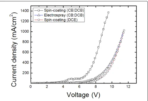
[image:3.595.58.537.387.703.2]To investigate the difference between electrospray and spin-coating processes, PVK thin films were formed by two different processes, and their electric and PL char-acteristics were investigated. As mentioned earlier, development of a proper solvent is an important step in
the electrospray process. Accordingly, we also investi-gated the effects of solvents on electric and PL film characteristics. Figure 4 shows the effects of solvents and process method on PL characteristics. We chose
[image:4.595.60.535.87.635.2]two different types of solvents: an aromatic solvent which comprised a mixture of CB and DCB and non-aromatic solvents, chloroform [CF] and 1, 2-dichlor-oethane [DCE]. The mixture of CB and DCB was
selected as it was optimum for our device structure and process. The PL peaks of the thin films were observed at 407 nm with CF and DCE and at 410 nm with the aromatic solvent mixture. Using the same aromatic sol-vent, PVK films processed by the electrospray process showed PL peaks at 407 nm, while those made by spin-coating showed PL peaks at 410 nm. Qian et al. [19] reported a peak shift of PVK due to polymer conforma-tion caused by the solvent effect. We believe that a similar polymer conformation effect results not only Table 2 Summary of device performances
Device Process Ink Solvent EML
(nm) Cd/A (max)
Lm/W (max)
1 Spin-coating Ink 1 CB 78 24 10
2 Electrospray Ink 1 CB/DCB (5:3) 100 15 6
3 Electrospray Ink 1 CB/DCB (5:3) 120 18 6.6
4 Electrospray Ink 2 CB/DCB (5:3) 70 18 7.5
5 Electrospray Ink 2 CB/DCB (5:3) 100 24 9.2
6 Electrospray Ink 2 CB/DCB (1:1) 103 23 8.6
EML, emissive layer; CB, chlorobenzene; DCB, dichlorobenzene.
[image:5.595.59.539.226.705.2]from the solvent, but also from the processing method as shown in this work. Figure 5 shows the current-vol-tage characteristics of the PVK film using different sol-vents and processing methods. At the same thickness, the thin films using the aromatic solvent (mixture of CB and DCB) showed a higher current density than those processed with the DCE nonaromatic solvent. In terms of processing methods, the PVK film processed with the electrospray method showed a lower current density than that of spin-coated ones. These results sug-gest that polymer conformation of PVK thin films was affected by the processing method as well as by the sol-vent’s molecular structure as also indicated in PL results in Figure 4. Based on these results, we speculate that the properties of thin films made by the electrospray process are similar to those of spin-coated films made with DCE.
Conclusion
We have demonstrated polymer organic LEDs using an electrospray process as a solution process alternative. Device performance comparable to spin-coating was
achieved with the electrospray process, which can be considered as a scalable large-area process alternative. However, the electrospray process requires elaborate choices involving solvents and higher concentrations of hole and electron transport materials in active materials. A high dielectric constant and a high-boiling point sol-vent like DCB are preferred in electrospray processing. Accordingly, the device based on the electrospray pro-cess had better performance when we used the ink hav-ing higher concentrations of hole and electron transport materials. The electrospray process can be considered as a viable solution for large-area organic thin-film forma-tion technology in the future.
Acknowledgements
This research was supported by the Basic Science Research Program through the National Research Foundation of Korea (NRF) funded by the Ministry of Education, Science and Technology (2011-0012279) and (2011-0006268).
Author details
1School of Chemical Engineering, Sungkyunkwan University (SKKU), Suwon,
440-746, South Korea2SKKU Advanced Institute of Nanotechnology (SAINT),
[image:6.595.61.539.86.414.2]Sungkyunkwan University (SKKU), Suwon, 440-746, South Korea
Authors’contributions
WH carried out the overall experiment. GX helped in the PL measurement. MC participated in the device fabrication. SMC and HC gave advice for this work. All authors read and approved the final manuscript.
Competing interests
The authors declare that they have no competing interests.
Received: 6 September 2011 Accepted: 5 January 2012 Published: 5 January 2012
References
1. Tang CW, VanSlyke SA:Organic electroluminescent diodes.Appl Phys Lett
1987,51:913-915.
2. Burroughes JH, Bradley DDC, Brown AR, Marks RN, Mackay K, Friend RH, Burns PL, Holmes AB:Light-emitting diodes based on conjugated polymers.Nature1990,347:539-541.
3. Baldo MA, O’Brien DF, You Y, Shoustikov A, Sibley S, Thompson ME, Forrest SR:Highly efficient phosphorescent emission from organic electroluminescent devices.Nature1998,395:151-154.
4. Baldo M, Deutsch M, Burrows P, Gossenberger H, Gerstenberg M, Ban V, Forrest S:Organic vapor phase deposition.Adv Mater1998,10:1505-1514. 5. Hebner TR, Wu CC, Marcy D, Lu MH, Sturm JC:Ink-jet printing of doped
polymers for organic light emitting devices.Appl Phys Lett1998,
72:519-521.
6. Pardo DA, Jabbour GE, Peyghambarian N:Application of screen printing in the fabrication of organic light-emitting devices.Adv Mater2000,
12:1249-1252.
7. Tseng S-R, Meng H-F, Lee K-C, Horng S-F:Multilayer polymer light-emitting diodes by blade coating method.Appl Phys Lett2008,
93:153308-153303.
8. Kopola P, Tuomikoski M, Suhonen R, Maaninen A:Gravure printed organic light emitting diodes for lighting applications.Thin Solid Films2009,
517:5757-5762.
9. O’Regan M:Solution processed OLED displays: advances in performance, resolution, lifetime and appearance.SID Symp Digest Tech Pap2009,
40:600-602.
10. Jin H, Sturm JC:Super-high-resolution transfer printing for full-color OLED display patterning.J Soc Inf Display2010,18:141-145. 11. Saf R, Goriup M, Steindl T, Hamedinger TE, Sandholzer D, Hayn G:Thin
organic films by atmospheric-pressure ion deposition.Nat Mater2004,
3:323-329.
12. Ju J, Yamagata Y, Higuchi T:Thin-film fabrication method for organic light-emitting diodes using electrospray deposition.Adv Mater2009,
21:4343-4347.
13. Kim J-S, Chung W-S, Kim K, Kim DY, Paeng K-J, Jo SM, Jang S-Y:
Performance optimization of polymer solar cells using electrostatically sprayed photoactive layers.Adv Funct Mater2010,20:3538-3546. 14. Wilhelm O, Mädler L, Pratsinis SE:Electrospray evaporation and
deposition.J Aerosol Sci2003,34:815-836.
15. Rietveld IB, Kobayashi K, Yamada H, Matsushige K:Electrospray deposition, model, and experiment: toward general control of film morphology.J Phys Chem B2006,110:23351-23364.
16. Jaworek A, Sobczyk AT:Electrospraying route to nanotechnology: an overview.J Electrostat2008,66:197-219.
17. Lide DR:Handbook of Organic SolventsBoca Raton: CRC Press; 1995. 18. Kim JW, Yamagata Y, Kim BJ, Higuchi T:Direct and dry micro-patterning
of nano-particles by electrospray deposition through a micro-stencil mask.J Micromechanics Microengineering2009,19:025021.
19. Qian L, Bera D, Holloway PH:Electrophosphorescence from triplet excimers in poly-(N-vinylcarbazole).Appl Phys Lett2007,90:103511-103513.
doi:10.1186/1556-276X-7-52
Cite this article as:Hwanget al.:Electrospray deposition of polymer thin films for organic light-emitting diodes.Nanoscale Research Letters 20127:52.
Submit your manuscript to a
journal and benefi t from:
7Convenient online submission
7Rigorous peer review
7Immediate publication on acceptance
7Open access: articles freely available online
7High visibility within the fi eld
7Retaining the copyright to your article