http://dx.doi.org/10.4236/jamp.2015.32030
A Study of Design Optimization Using
Response Surface Analysis and Fabricaiton
MEMS Probe Tip
K. B. Kim1, J. W. Lee1, S. J. Ha1, Y. K. Cho1, M. W. Cho2
1Department of Mechanical Engineering, Inha University, Incheon, Republic of Korea 2Division of Mechanical Engineering, Inha University, Incheon, Republic of Korea
Email: [email protected]
Received 17 December 2014
Abstract
In semiconductor manufacturing process, probe station that is testing equipment is important. Inspection step is for detecting defects on semiconductor before the packaging. Probe card is a part of probe station and contains probe tip that contacts to semiconductor. Through probe tip, it can inspect defects of semiconductor. In this paper, optimization method is used with response surface analysis to design MEMS type probe tip. And fabricating probe tip uses maskless lithogra-phy, electro-plating and lapping process.
Keywords
Probe Tip, Semiconductor, Maskless Lithography, Response Surface Analysis, Optimization
1. Introduction
Recently, semiconductor technology develops to highly integrate and compact. So testing process for semicon-ductor is also developed [1]. Probe station is test equipment for chips on wafer, using probe tip involved in probe card for testing [2]. Probe card can be classified into cantilever, vertical and MEMS (Micro Electro Me-chanical System) types [3]. In this paper, we design MEMS type probe tip using optimization method with re-sponse surface analysis and fabricate probe tip through maskless lithography, electro plating and lapping process.
2. Probe Tip Design Optimization Using Response Surface Analysis
2.1. Probe Tip Design and Structure AnalysisFor proper performance of probe tip, few conditions are needed. Not damage to semiconductor, enough dis-placement for contact with semiconductor, superb fatigability that is caused from repeat motion, and good elec-trical conductivity for transmit elecelec-trical ignal. Additional, probe tip is needed more than 2 gf contact force for stable contact with semiconductor [34].
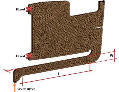
structure analysis for optimization with response surface analysis. We design probe tip as shown Figure 1. The basic size of probe tip are L = 2.0 mm, W = 0.2 mm, T = 0.045 mm and progress structure analysis. We fabri-cate probe tip using electro plating with Nickel, so properties of probe tip that we made are different from gen-eral Nickel materials. From this reason, we measured properties of Nickel that made from electro plating and use these data for analysis [5]. The value of electro plating Nickel is shown as Table 1.
Mesh and boundary condition of analysis is shown as Figure 2. Fixed points are part that adhere to interposer and vertical displacement point is bottom of cantilever beam that contact with semiconductor. Under these con-ditions, we confirm stress distribution of probe tip cause from vertical over drive. Structure analysis mesh is 50 um tetrahedrons mesh
[image:2.595.187.416.254.431.2]Form the result of structure analysis, maximum stress occur at the point that is linked with main body of probe tip and maximum strength is 751.48 MPa. This value is under the yield strength of Nickel, so probe tip that we design is suitable. But we cannot assure this design is best, so progress optimization of probe tip using response surface analysis.
Figure 1. Figure and mesh of probe tip.
[image:2.595.122.476.459.708.2]2.2. Design Optimization of Probe Tip
[image:3.595.98.528.196.576.2]For design optimization use analysis software Ansys 14.5. Design variables range are length 2.0 - 2.5 mm, width 0.15 - 0.20 mm, thickness 0.045 - 0.050 mm, over drive 100 um displacement as shown in Table 2. Use two boundary conditions for optimization minimum contact force 2 gf and yield strength of nickel 860 Mpa.
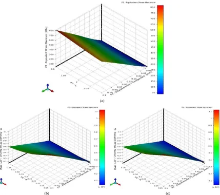
Figure 3 are results of response surface analysis stress and contact force by length, width and thickness. First, in case of stress, as over drive increase, length, width and thickness are also increased (Figure 4). As length in-crease, stress is decreased and the width is boarder, the stress is bigger. But as thickness inin-crease, stress is de-creased till 0.0475 mm and after that point stress is inde-creased.
(a)
(b) (c)
[image:3.595.87.539.620.655.2]Figure 3. Results of equivalent stress of parameters. (a) Stress by length; (b) Stress by width; (c) Stress by thickness.
Table 1. Material properties of nickel.
Density Modulus of Elasticity Tensile Strength Poisson’s Ratio
[image:3.595.90.539.683.717.2]8.90 g/cm3 169 Gpa 882.7 Mpa 0.31
Table 2. Range of design parameters.
Length Width Thickness Over Drive
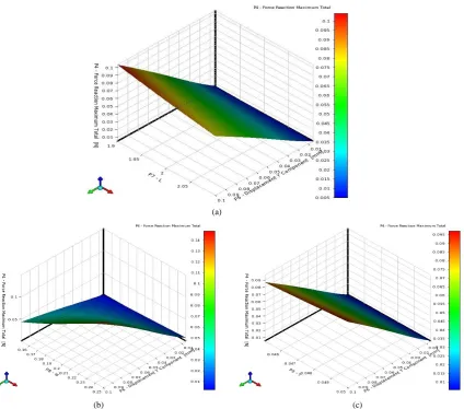
Second, in case of contact force, over drive increase, length, width and thickness are also increased. In each case, contact force increase when length is shorter, width is boarder and thickness is thicker. Figure 5 shows in-fluence of each variables to stress and contact force and priority of inin-fluence of variables is over drive > width > length > thickness. This tendency is similar to case of cantilever beam in material mechanics.
Table 3 is 3 optimum condition cases that are drawn using response surface analysis and through this ten-dency, confirm fabrication possibility of probe tip.
3. Fabrication of Probe Tip
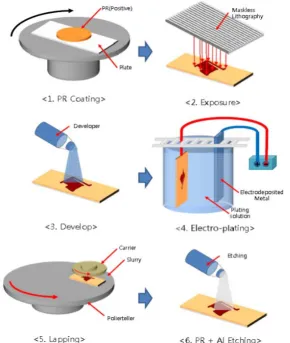
Probe tip fabrication process is as shown Figure 6. First, PR (Photo Resist, AZ4620) coating on Al plate with thickness 50 um and making a pattern that use maskless lithography system. Next, remove pattern that made by lithography with developing process and nickel plating on Al plate with the way of electro plating. After electro plating, lapping the nickel. Through this process thickness of nickel is 49 um. And using etching process to di-vide probe tip with Al plate.
[image:4.595.99.524.318.692.2]Maskless lithography system that is used for fabricating probe tip is DMD type and exposure UV light source on pattern image. Image format is Bitmap Through this system, we fabricate blade probe tip type patterns.
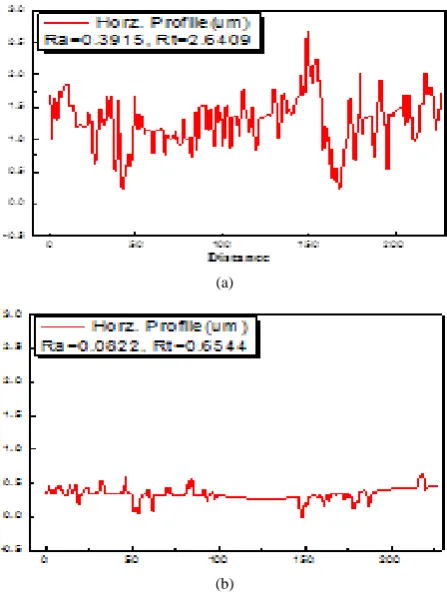
Figure 7 is shown surface roughness of nickel before and after lapping. Surface roughness values at before lapping are Ra = 0.3915 um, Rt = 2.6409 um and at after lapping are Ra 0.0822 um, Rt = 0.6544. From these results, we can confirm improvement of surface roughness through lapping.
(a)
(b) (c)
Figure 5. Influence of parameters to stress and contact force.
[image:5.595.156.447.361.705.2](a)
[image:6.595.185.409.84.384.2](b)
Figure 7. Surface roughness on nickel.
Table 3. Case of optimization result.
Over drive Length Width Thickness Stress Reaction force
Unit mm gf
Case. 1 0.089 1.93 0.22 0.0492 859.0 12.26
Case. 2 0.077 1.94 0.24 0.0494 834.8 11.91
Case. 3 0.097 1.99 0.21 0.0494 842.5 11.64
4. Conclusions
In this paper, we fabricate probe tip that is used at test process to semiconductor. Optimization method using re-sponse surface analysis is used for design of probe tip and fabricate processes are used for electro-plating and maskless lithography system. Through this paper, we can confirm possibility of applying to probe tip. The paper contents are as follows.
1) Fabricate nickel thin film with electro-plating used for probe tip fabrication.
2) We confirm properties of the electro-plating nickel like hardness, modulus and yield strength. The yield strength value is 882.7 Mpa.
3) Through characterization of nickel that is fabricated using electro plating, it differs from general nickel properties. So we use properties of nickel using electro-plating that we measure.
4) To fabricate probe tip, use maskless lithography system through exposure probe tip figure pattern on pho-toresist.
5) Through lapping process, adjust thickness of probe tip and improve surface condition. Also, lapping occurs on micro-work hardening on nickel.
Acknowledgements
[image:6.595.88.541.425.492.2]References
[1] Ha, S.J., Kim, D.W., Shin, B.C., Cho, M.W. and Han, C.S. (2010) Assessment of Design and Mechanical Characteris-tics of MEMS Probe Tip with Fine Pitch. Journal of Academia-Industrial Technology, 11, 1210-1215.
[2] Leslie, B. and Matta, F. (1989) Wafer-Level Testing with a Membrane Probe. IEEE Design & Test of Computers, 6, 10-17.
[3] Min, C.H. (2007) Fabrication of Vertical Type Probe Card and MEMS Probe Card for Wafer Level Chip Test. Catholic University.
[4] Kendall, D.L. (1975) On Etching Very Narrow Grooves in Silicon. Appl. Phys. Lett., 26, 195-198. http://dx.doi.org/10.1063/1.88113