http://dx.doi.org/10.4236/cs.2016.79213
Incorporation of Reduced Full Adder and
Half Adder into Wallace Multiplier and
Improved Carry-Save Adder for
Digital FIR Filter
S. Chinnapparaj
1, D. Somasundareswari
21Department of ECE, Hindusthan Institute of Technology, Coimbatore, India 2Department of EEE, SriGuru Institute of Technology, Coimbatore, India
Received 10 February 2016; accepted 17 March 2016; published 22 July 2016
Copyright © 2016 by authors and Scientific Research Publishing Inc.
This work is licensed under the Creative Commons Attribution International License (CC BY). http://creativecommons.org/licenses/by/4.0/
Abstract
Improvement of digital FIR filter is vital in the field of Digital Signal Processing in order to reduce the area, delay and power. Multiplication and Accumulation (MAC) unit of Finite Impulse Response (FIR) filter has been designed using efficient multiplier and adder circuits for optimized APT (Area, Power and Timing) product. In this paper, the design of direct form FIR filter with efficient MAC unit has been presented. Initially, full adder and half adder structures are shrunk down by reduc-ing number of gates. These compact full adder and half adder structures are incorporated into Wallace Multiplier and Improved Carry-Save Adder. The proposed 16-bit Carry-Save Adder has been improved by splitting into four parallel phases. Consequently the delay of enhanced Carry- Save Adder is reduced. Generation of carry output is performed using number of OR gates in a se-quential manner. All these enhanced architectures are incorporated into the Digital FIR Filter to reduce the area, delay and power utilization.
Keywords
Direct Form FIR Filter, Compact Full Adder and Half Adder, Improved Carry-Save Adder, Modified Wallace Multiplier, FPGA
1. Introduction
applica-tions of digital signal processing. When it provides limited power and area, it is extensively used in several portable applications [1]. The two fundamental FIR structures used for a linear phase FIR filter are transposed form and direct form. In this paper, direct form digital FIR filter is used for DSP applications. Multiplier-Ac- cumulator (MAC) unit of FIR filter is the most important element. The efficiency of the MAC unit is affected by full adder. Full adder circuit power reduction is necessary for low power application. The heart of the processor is Arithmetic & Logic Unit (ALU) [2]. It contains elements for reckoning operations. It plays a very important role in computation time of the processor. Multiplication operation is more recurrent in Digital Signal Processing (DSP) application. Sinking delay in the multiplier shrinks the overall computation time [3]. One of the fast multipliers is available such as Wallace multiplier. It works due to speeding up the addition process. Carry Propagating Adder has been used to sum the final two rows. A direct implementation needs a (2N − 2) bit Carry Propagating Adder (CPA), where N is the number of bits of operands. Carry Propagating Adder obtains long time when the carry is required to get promulgated until the last adder [4]. In this work, a fast carry-save adder is implemented at the last stage to obtain superior performance.
Modified Carry-Save Adder consumes more delay and area due to propagation delay and sequential process
[5]. Hence Improved Carry-Save Adder (ICSA) is designed in this work with parallel processing and without carry propagation delay. Our ICSA adder offers less area and higher speed than all other schemes. Regular Wal-lace and reduced WalWal-lace Multipliers are designed using different high speed adders [6]. But it consumes more area, power and less delay [7]-[9]. So compact full adder, half adder and ICSA adder are incorporated into Wal-lace to improve the efficiency of our multiplier. Several previous endeavors for reducing area, delay and power consumption of digital FIR filter usually focus on the optimization of the filter coefficient while the filter order is fixed [10]. FIR filter structures are simplified to, minimizing the number of additions/subtractions & Add and Shift operations which is the main focus of those approaches. However, one of the drawbacks encountered in those approaches is that once the filter architecture is determined, the coefficients cannot be altered [11]. Con-sequently, those schemes are not appropriate to the FIR filter with programmable coefficients [12]. Reconfigur-able FIR filter with modified Amplitude Detector (AD) and control logic is introduced to reduce the area and power utilization [13]. But it makes performance degradation. Previously described works have been focused on reducing the power consumption and improving the configuration of filter coefficients. However, all those ar-chitectures have more complexity, because of using traditional hardware structures to perform multiplication and accumulation functions. In order to reduce the hardware complexity of MAC unit, redundant logical func-tions are identified with the help of Boolean expressions. It is identified that half adder and full adder are used in every digital signal processing operation like MAC and ALU. Hence, the redundant Boolean logical expressions of half adder and full adder are identified to optimize the digital signal processing operations. So our proposed Direct FIR filter offers optimum area, delay and power compared with the all other filter techniques also without any degradation. Because Enhanced Wallace Multiplier with Improved Carry-Save adder is incorporated into proposed FIR filter.
The rest of the paper is organized as follows. The optimization procedure for full adder and half adder is ex-plained in Section 2. This section clearly explains the identification of the redundant Boolean expression logics and optimization procedure. In Section 3, procedure for designing improved carry-save adder is involved with the help of modified Binary to Excess I conversion process. In Section 4, incorporation of designed reduced full adder and half adder into reduced Wallace tree multiplier is explained briefly. Section 5 explains the block dia-gram of direct form FIR filter and incorporation methods of reduced full adder and half adder into FIR filter. Synthesis results of proposed multiplication and filter are analyzed in Section 6 and Section 7 concludes that ICSA based digital FIR filter is the best option for digital signal processing applications.
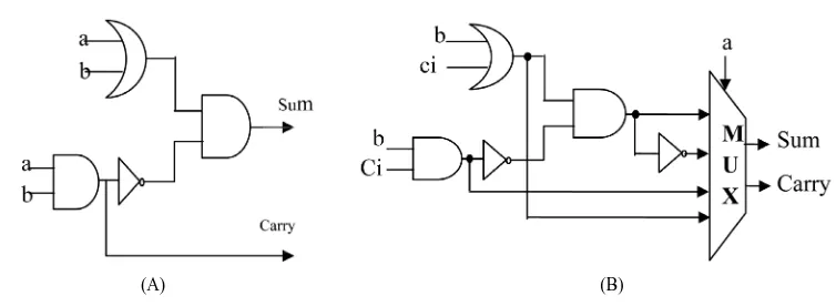
2. Reduced Full Adder and Half Adder Structure
(A) (B)
Figure 1. Structures of reduced half adder and full adder. (A) Reduced half adder; (B) Reduced full adder.
Reduced Half Adder structure is simplified by use of Demorgan’s theorem and some Boolean logic. General expression to find the sum of half adder is given in Equation (1)
(
)
(
) (
) (
)
(
)
(
)
Sum AB BA
A B A B A A B B
A B A B
= +
= + ⋅ + ⋅ + ⋅ +
= + +
(1)
(
)
Sum= A+B ⋅AB (2)
Carry= ⋅A B (3)
Equations (2) and (3) are simplified Sum and Carry Expression for reduced half adder. Similarly Full adder is shrinking down by introducing Boolean logic and Demorgan’s Law.
Simplified expression of Sum and Carry of compact Full Adder are given in Equation (4) and Equation (5) which is derived as below.
1
0
A
Sum X A XA
=
=
∑
⋅ + (4)where
(
)
(
)
(
)
X B C BC BC CB B C
X B C BC BC CB BC BC B C
= + ⋅ = + = ⊕ = + ⋅ = + = + = ⊕
(
)
1 0 ACarry BCA B C A
=
=
∑
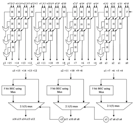
+ + (5)3. Improved 16-Bit Carry-Save Adder
Conventional 16-bit Carry-Save Adder has been designed in the sequence manner. Hence the propagation delay of this adder is high. It has 15-full adders and 17-half adders. As the ripple carry adder is used in the last phases, this architecture yields maximum carry propagation delay [4] and [14]. To minimize this delay, the last stage of CSA is separated into five sets. After splitting into 5 stages, chip size (area) and power utilization is maximum in the existing CSA. Consequently this structure is split into four stages and parallel processing is performed in order to achieve less delay, area and power than the existing CSA. Construction of Improved Carry-Save Adder (ICSA) is shown in Figure 2. Enhanced 16-bit Carry-Save Adder consists of number of half adder, OR gate, 5-bit BEC & 2:1 MUX. The divided four groups of ICSA are listed below [5],
[image:3.595.121.498.80.218.2]Figure 2. Architecture of enhanced 16-bit carry-save adder using modified 5-bit BEC structure and parallel processing.
The 1st group of output s[3:0] are straightforwardly assigned as the final output; the 2nd group {c1,x[7:4]} controls the fractional result by allowing for c1 is 0; the 3rd group {c2,x[11:8]} influences the partial result through thinking c2 is 0; the 4th group {c3,x[12:15]} maneuvers the FPGA Implementation of partial result by considering c3 is 0.
Improved Carry-Save Adder is designed by using the below Equations (6) to (10) which are obtained from the
Figure 2.
0 0 0
s =a ⊕b (6)
1 0 0
s =x ⊕c (7)
(
)
2 1 1 0 0
s = ⊕ ⊕x c x ⋅c (8)
(
) (
)
3 2 3 1 1 1 1 2
s =x ⊕ ⊕c x c⋅ ⊕ x ⊕c ⋅c (9)
(
) (
)
{
(
) (
) (
)
}
4 6 2 3 2 3 1 1 2 3 1 1 1 1 0 0
s =c + x ⋅c + x ⊕c ⋅x c+ x ⊕ ⊕c x c⋅ ⋅ x ⊕c ⋅ x ⋅c (10)
0 1 1
1 2 2
2 3 3
0 0 0
x a b
x a b
x a b
c a b
= ⊕
= ⊕
= ⊕
= ⋅
1 1 1
2 0 0
3 2 2
4 1 1
c a b
c x c
c a b
c x c
= ⋅ = ⋅ = ⋅ = ⋅
(
)
5 1 1 2 6 3 3
c x c c
c a b
= ⊕ ⋅
= ⋅
(
)
7 2 3 8 2 3 4
c x c
c x c c
= ⋅
= ⊕ ⋅
(
)
9 2 3 4 5
c = x ⊕ ⊕c c ⋅c
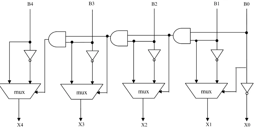
Depending on c0 of the 1st group, the 2nd group mux provides the last result without the carry propagation de-lay from c1 to c2; depending on c2 of the second group final result, the 3rd group mux offers the final result without the carry propagation delay from c2 to s16. The major advantage of this logic is that every group calcu-lates the limited results in parallel and the muxes are prepared to provide the last result without any delay of the mux. Once the Cin of every group enters, the last result will be find instantaneously. Modified 5-bit BEC struc-ture is shown in Figure 3 which consists of four modified XOR gate structures are connected in sequential or-der.
4. Enhanced Wallace Multiplier
In this work, the design of Enhanced Wallace Multiplier with improved Carry-Save Adder is performed to eva-luate best APT (Area, delay and timing) reduction. Proposed Wallace multiplier is designed by introducing the compact full adder, half adder and improved carry-save adder structures. Hence the proposed Wallace multiplier provides less area, delay and power than the existing Wallace multiplier techniques [9].
The adapted version of Wallace multiplier is called as Enhanced Wallace multiplier. It contains a less amount of half adders when compared to the regular Wallace multiplier is shown in Figure 4. Partial products are created through N2 AND gates and they are located in an inverted triangle manner, which is separated into three row clusters in the modified Wallace reduction method [14] and [15].
1) Group of three bits are summed by applying a full adder.
2) Single bit and a group of 2 bits are stimulated to the next stage straightforwardly.
[image:5.595.94.531.479.704.2]The Improved Carry-Save Adder (ICSA) with modified 5-bit BEC is incorporated in the final stage with the aim of low area, power and delay utilization. Enhanced Wallace Multiplier with Improved Carry-Save Adder
Figure 4. Reduced complexity Wallace multiplier.
(ICSLA) provides less area, delay and power than all other schemes which is confirmed by the results that fol-low. The enhanced Wallace Multiplier is applied in Digital FIR filter to analyze the efficiency of proposed me-thods. MAC unit of Digital FIR filter is vital for coefficient multiplication and addition. These efficient adders and Multipliers are integrated into MAC unit of the proposed Direct FORM FIR filter. The proposed FIR filter with Wallace Multiplier and Improved Carry-Save Adder (ICSA) is better for optimized APT product.
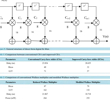
5. Proposed Direct Form Digital Fir Filters
FIR filter circuit must be able to drive at high sample rates, whereas in extra applications, the FIR filter archi-tecture must be a low-power circuit operating at moderate sample rates [16]. The low-power or low-area schemes developed particularly for digital filters. In order to further increase the effective throughput, decrease the power utilization and area of the original filter. Parallel processing can be applied to digital FIR filters. Di-rect Form Digital FIR filter is shown in Figure 5 which consists of delay unit, adder and multiplier units in the sequential manner [17].
In this paper, the design of Enhanced Wallace Multiplier with Improved Carry-Save Adder is presented. This effective multiplier is applied in Direct Form FIR Filter structure to analyze the Area, Power and Timing prod-uct. Proposed Direct Form FIR filter with enhanced Wallace Multiplier provides less area, power and delay than regular Direct Form FIR Filter.
6. Results and Discussion
to analyze the APT product as shown in Table 1. From the results, Improved Carry-Save Adder offers 25% area reduction and 15% delay reduction compared to conventional Carry-Save Adder.
Total equivalent LUT in case of enhanced Wallace multiplier with CSA is 162, which is improved to 152 us-ing Improved Carry-Save Adder based Wallace Multiplier. The power consumption in case of enhanced Wallace multiplier with CSA is 264 mW, which is improved to 252 mW using ICSA based Wallace multiplier. The number of occupied slices used in enhanced Wallace multiplier with ICSA is also reduced. In case of reduced Wallace multiplier with Carry-Save Adder it is 87 and in enhanced Wallace multiplier with ICSA it is 79. En-hanced Wallace multiplier results are tabulated as shown in Table 2.
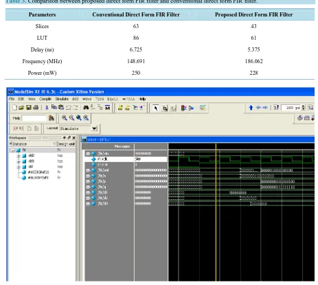
From the outcomes, Proposed Direct Form FIR Filter with Enhanced Wallace Multiplier provides 50% area reduction and 12% power reduction compared to conventional Direct Form FIR Filter and frequency utilization of proposed FIR Filter is improved up to 38%. Simulation result of proposed digital FIR filter is validated by using ModelSim 6.3C design tool. Simulation result of proposed digital FIR filter is shown in Figure 6. Table 3
shows the Comparison between proposed direct form FIR filter and conventional direct form FIR filter.
[image:7.595.97.514.320.508.2]As shown in Figure 6, data input (xin) is given as 8’d50 (00110010). The finite impulses are determined with the help of proposed MAC unit. Three constant filter coefficients are considered in the current research work such as 8’d5, 8’d2 and 8’d3 respectively. Hence, output is generated as 8’d250 (8’d50*8’d5), 8’d350 ((8’d50*8’d5) + (8’d50*8’d2)) and 8’d500 ((8’d50*8’d5) + (8’d50*8’d2) + (8’d50*8’d3)) respectively, which are shown in Figure 6. Similarly, for other combination of inputs, output parameters are validated.
Figure 5. General structure of direct form digital fir filter.
Table 1. Comparison between conventional CSA and improved CSA.
Parameters Conventional Carry-Save Adder (CSA) Improved Carry-Save Adder (ICSA)
Delay (ns) 23.854 20.655
Slices 40 32
[image:7.595.98.536.324.722.2]LUT 71 57
Table 2. Comparison of conventional Wallace multiplier and modified Wallace multiplier.
Parameters Reduced Wallace Multiplier Modified Wallace Multiplier
Slices 87 79
LUT 162 152
Delay (ns) 21.867 18.718
[image:7.595.88.542.643.722.2]Table 3. Comparison between proposed direct form FIR filter and conventional direct form FIR filter.
Parameters Conventional Direct Form FIR Filter Proposed Direct Form FIR Filter
Slices 63 43
LUT 86 61
Delay (ns) 6.725 5.375
Frequency (MHz) 148.691 186.062
Power (mW) 250 228
Figure 6. Simulation result of proposed digital FIR filter.
7. Conclusion
In this paper, high-speed and area-efficient Reduced Full Adder, Half Adder, Improved Carry-Save Adder (ICSA) and modified 5-bit BEC (Binary to Excess one code Converter) using mux are presented. Reduced full adder and half adder are designed using less number of gates compared with conventional full adder and half adder. These reduced adders are applied in the Wallace Multiplier to analyze the performance. After generating the partial product, Improved Carry-Save Adder (ICSA) with modified 5-bit BEC is applied to further reduce the area and delay. Enhanced Wallace Multiplier with Improved Carry-Save Adder is incorporated into Direct Form Digital FIR filter to examine the performance. Proposed Direct Form FIR filter offers less area, power and high-er speed compared with conventional Direct Form FIR filthigh-er. This filthigh-er can be used in wireless communication techniques, signal processing and image processing mechanisms.
References
[1] Parhi, K.K. (1998) VLSI Digital Signal Processing. Wiley, New York.
[3] Kharate, A.B. and Gumble, P.R. (2013) VLSI Design and Implementation of Low Power MAC for Digital FIR Filter.
International Journal of Electronics Communication and Computer Engineering, 4, REACT-2013.
[4] Parhami, B. (2010) Computer Arithmetic: Algorithms and Hardware Designs. 2nd Edition, Oxford University Press, New York.
[5] Ramkumar, B., Kittur, H.M. and Mahesh Kannan, P. (2010) ASIC Implementation of Modified Faster Carry-Save Ad-der. European Journal of Scientific Research, 42, 53-58.
[6] Gowrishankar, V., Manoranjitham, D. and Jagadeesh, P. (2013) Efficient FIR Filter Design Using Modified Carry Se-lect Adder & Wallace Tree Multiplier. International Journal of Science, Engineering and Technology Research, 2, 703- 711.
[7] Kannan, N., Seshadri, R. and Ramakrishnan, S. (2014) Improved Wallace Tree Multiplier Based Direct Fir Structure Using MCM Technique. Proceedings of ICSEM’14-2nd International Conference on Science, Engineering and
Man-agement, March 2014.
[8] Gnanasekaran, M. and Manikandan, M. (2014) Performance of FIR Filter with Wallace Multiplier over FIR Filters with Truncated Multiplier. International Journal of Computer Science and Engineering Communications, 2, 450-455. [9] Waters, R.S. and Swartzlander, E.E. (2010) A Reduced Complexity Wallace Multiplier Reduction. IEEE Transactions
on Computers, 59, 1134-1137. http://dx.doi.org/10.1109/TC.2010.103
[10] Kashyap, S. and Maheshwari, M. (2014) Implementation of High Performance Fir Filter Using Low Power Multiplier and Adder. International Journal of Engineering Research and Applications, 4, 177-181.
[11] Aksoy, L., Lazzari, C., Costa, E., Flores, P. and Monteiro, J. (2013) Design of Digit-Serial FIR Filters: Algorithms, Architectures, and a CAD Tool. IEEE Transactions on Very Large Scale Integration (VLSI) Systems, 21, 498-551.
http://dx.doi.org/10.1109/TVLSI.2012.2188917
[12] Hsiao, S.-F., Zhang Jian, J.-H. and Chen, M.-C. (2013) Low-Cost FIR Filter Designs Based on Faithfully Rounded Truncated Multiple Constant Multiplication/Accumulation. IEEE Transactions on Circuits and Systems II: Express Briefs, 60, 287-291. http://dx.doi.org/10.1109/TCSII.2013.2251958
[13] Lee, S.-J., Choi, J.-W., Kim, S.W. and Park, J. (2011) A Reconfigurable FIR Filter Architecture to Trade off Filter Performance for Dynamic Power Consumption. IEEE Transactions on Very Large Scale Integration (VLSI) Systems,
19, 2221-2228. http://dx.doi.org/10.1109/TVLSI.2010.2088142
[14] Anju, S. and Saravanan, M. (2013) High Performance Dadda Multiplier Implementation Using High Speed Carry Se-lect Adder. International Journal of Advanced Research in Computer and Communication Engineering, 2, 1572-1575. [15] Ambika, R. and Siva Ranjani, S. (2014) Design of Fir Filter Using Area and Power Efficient Truncated Multiplier.
In-ternational Journal of Engineering Sciences & Research Technology (IJESRT).
[16] Blad, A. and Gustafsson, O. (2010) Redundancy Reduction for High-Speed FIR Filter Architectures Based on Car-ry-Save Adder Trees. Proceedings of 2010 IEEE International Symposium on Circuits and Systems, Paris, 30 May- 2 June 2010, 181-184. http://dx.doi.org/10.1109/ISCAS.2010.5537997
[17] Thakur, R. and Khare, K. (2013) High Speed FPGA Implementation of FIR Filter for DSP Applications. International Journal of Modeling and Optimization, 3, 92-94.