RAAR Processor: The Digital Image Processor
Raghumanohar Adusumilli1, Mahesh.B.Neelagar2
1
VLSI Design and Embedded Systems, Visvesvaraya Technological University, Belagavi
Abstract— Image processing have wide applications in the day to day life of humans in one or the other applications like Surveillance, multimedia applications, medicine, automobiles, authentication systems etc. The research in the domain of research happening now may lead to develop more and more application specific systems, which may change the way of living of humankind in the future. On the other hand FPGA’s (Field Programmable Gate Array) are one of the easy to implement and reconfigurable systems available for implementing signal processing and point processing operations because of their architectures. Implementing the image processing systems on a computer is an easier operation but not an effective solution, because of its constraints about memory and other peripherals. However there are very less number of general purpose image processors which can prove themselves as an efficient solution for this problem. The aim of this project is to design a digital image processor which can perform some of the basic image pre-processing operations like thresholding, contrast manipulation, grey to binary conversion etc. implemented using Verilog HDL in Xilinx ISE Project navigator targeting Spartan 6 Xilinx device.
Keywords— Digital Image Processor, FPGA, General purpose image processor.
I. INTRODUCTION
Image processing is just like any other form of signal processing but here the input is an image. The output of image processing can be an image or a set of characteristic information related to the image. Image processing is the process of manipulating the information which is in the form of image in order to derive specific results. In image processing there are two vital steps and they are image enhancement and information extraction. Image enhancement the name itself explains, it is all about enhancing or improving the visibility of any part of image. There are many techniques available to perform image enhancement and mainly the techniques are all about highlighting some features or supressing some features of interested region within an image. Further image enhancement can be categorised into two based on the domain in which enhancement can be applied
A. Spatial Domain
B. Frequency Domain
II. PAGELAYOUT
RAAR Image processor implementation is divided into three parts of design: Design of EU (Execution Unit)
Design of CU (Control Unit) Design of MU (Memory Unit)
The name of the processor is chosen on designer interest. The Processor is designed for implementing Low-Level image processing operations. The proposed processor architecture is as shown in Fig.1
The RAAR Processor includes following blocks as shown in Fig.1: Interface Unit
Interlace Unit Control Unit
Operation or Execution Unit Memory Units (M1,M2 and M3)
Fig.1 Proposed RAAR Image Processor Architecture
A. Execution Unit
Execution unit of the Application specific processor is important among all the other blocks, this is very similar to ALU unit in general purpose processors. This block in the processor is responsible in executing the various Low-Level Image processing operations. Image processing operations can be further classified into Monadic and Diadic operations. Monadic operations are the operations executed on single image. Diadic operations, are the operations performed on two images. Fig.2 and Fig.3 Show the block diagram of monadic and dyadic operations.
Image Monadic operations, each output pixel is nothing but the function operated on the input pixel of input image. Diadic operation each output pixel is a function operated on two input images, provided function applied is same for the entire image. The functions which comes under the category of monadic functions are usually image enhancement operations. In dyadic operation both the images should be of same size. An example for dyadic operation is image differencing. Here, In this custom processor design the operations considered to including in the processor are as follows:
1) Monadic Operations
2) Brightness Manipulation
8) Gray to Binary Conversion
9) Negative of Image
10) Range Highlighting
11) Image Segmentation using thresholding
12) Diadic Operations
13) Image addition
14) Image Subtraction
The approach used for implementing the entire processor Bottom-up design flow and the coding style opted is data flow.
Fig.2 Image Monadic operations
Fig.3 Image Diadic operations
B. Interlace Unit
Interlace unit is a register which converts the data from serial to parallel, Parallel to serial and also provides serial in serial out, parallel in parallel out. Interlace unit implements the parallelism in transferring the data too and fro between the memory and the external interface. When the image data is sent in the form of pixels serially one after the other. Interlace unit acts a intermediate block in converting the pixel data from serial to parallel.
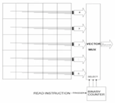
Memory is arranged is an array of sequential row having a cell component to save pixel value. Entire image can be stored on this network. There are totally three memory blocks in the architecture, two are write memory and the remaining one block is read memory. Write memory block stores the pixel values of input images and read memory block is to store the processed resultant image. The input data path is connected to write memory blocks and the output data path passes through the read memory block. Read and write operations for indexing both read and write memory blocks, indexing pointers get updated after each row operation on the image. The pixels are 8 bit wide, interface unit read in the pixel values and interlace coverts them into parallel, later entire set of pixels are transferred into memory. Fig. 4 (a) and 4 (b) shows the block diagram representation of the write and read memory blocks. Data transfer takes place row wise into memory, on every clock pulse. This is how concept of parallelism is introduced in the architecture.
Fig. 4 (a) Write memory block diagram
Fig.4 (b) Read memory block diagram
III. RESULTS
[image:5.612.221.412.219.390.2] [image:5.612.204.392.385.579.2]processor in both Matlab and FPGA environment.
Operation Matlab FPGA Implementation
Brightness Manipulation 12.230µs 4.248ns
Contrast Manipulation 13.793µs 7.258ns
Gray to Binary 6.428µs 3.820ns
Image Negative 3.372µs 4.009ns
Range Highlighting 3.204µs 7.446ns
Image Segmentation 4.023µs 5.837ns
Image Addition 3.784µs 4.224ns
Image Subtraction 3.662µs 4.124ns
Table.1 Table listing the delay details per pixel
Operation Opcode Name
Binary two gray 0000 b2g
Negative 0001 Neg
Range Highlighting 0010 Rang
Segmentation 0011 Seg
Contrast Adjustment 0100 Cont
Brightness Increase 0101 Briti
Brightness decrease 0110 Britd
Image addition 0111 Imad
Image Subtraction 1000 imsb
Table.4.2 List of opcodes and function names
0
2
4
6
8
10
12
14
16
DELAY COMPARISON
Matlab in µs
FPGA in ns
Fig.5 Graph relating the time taken to implement the operation per pixel in Matlab and FPGA environment
Fig.7 Output waveforms of the proposed RAAR Processor
IV. CONCLUSIONS
The RAAR processor proposed was designed for FPGA implementation capable of performing low end image processing operations. The operations of the EU unit of the proposed digital image processor were also implemented using Matlab and a comparison is brought out to highlight the capacity of the processor implemented on FPGA. The proposed architecture is reconfigurable in nature, the design is capable to handle smaller images and the same can be extended for larger resolution images with small changes. The design is implemented completely using Xilinx 14.7, the intention was to avoid the use of Matlab system generator and is achieved. From the results it can be quoted that, the FPGA based digital image processor for image processing applications are better than implementing the same on Matlab, in terms of delay. In future the processor architecture can be further modified and to develop pipelining architecture and along with that Mid-level image processing operations can be included as a part of this. Application oriented image processing deigns can be developed with the use of this or the modified architecture. There is a necessity to have a general image processors which can come in future. The architecture can also be developed considering asynchronous logic style.
REFERENCES
[1] Shanthi K J, Ashok L R, Anandu A S and Gokul Das B “FPGA Implementation of Image Segmentation Processor”, Second International Conference on
Emerging Trends in Engineering and Technology, ICETET-09.
[2] Mohamed Nasir Bin Mohamed Shukor, Lo Hai Hiung , Patrick Sebastian, “Implementation of Real-time Simple Edge Detection on FPGA ” International
Conference on Intelligent and Advanced Systems 2007.
[3] Ms. Dipika S.Warkari, Dr.U.A.Kshirsagar, “FPGA Implementation of Point Processing Operation using Hardware Simulation ”, International Journal of
Advanced Research in Computer and Communication Engineering Vol. 4, Issue 4, April 2015.
[4] V.Balaji, R.Krishnaveni, “fpga based low complexity multipurpose reconfigurable image processor”, icices2014 - S.A.Engineering College, Chennai, Tamil Nadu, India, ISBN No.978-1-4799-3834-6, 2014, IEEE.
[5] Mohamed Nasir Bin Mohamed Shukor, Lo Hai Hiung, Patrick Sebastian, “Implementation of Real-time Simple Edge Detection on FPGA”, International
Conference on Intelligent and Advanced Systems 2007, IEEE.
[6] Emerson Carlos Pedrino, Marcio Merino Fernandes, “Automatic Generation of Custom Parallel Processors for Morphological Image Processing”, 2014
IEEE 26th International Symposium on Computer Architecture and High Performance Computing, IEEE.
[7] Renuka, Jenitha A, “Implementation of image processing algorithm using partial dynamic reconfiguration in fpga”, International Journal For
Technological Research In Engineering Volume 2, Issue 9, May-2015.
[8] Iuliana CHIUCHISAN, Marius CERLINCA, Alin-Dan POTORAC, Adrian GRAUR, “Image Enhancement Methods Approach using Verilog Hardware
Description Language” 11th International Conference on development and application systems, Suceava, Romania, May 17-19, 2012, IEEE.
[9] K. Anil Kumar and M. Vijay Kumar, “Implementation of Image Processing Lab Using Xilinx System Generator”, Advances in image and video
processing, Volume 2, Issue 5, 2015.
[10] Emerson Carlos Pedrino, Marcio Merino Fernandes, “Automatic Generation of Custom Parallel Processors for Morphological Image Processing”, 2014