A High Slew Rate Buffer Amplifier Employing MTCMOS
Technique for Flat Panel Display
Ajay Yadav
Research Scholar ITM Gwalior, India
Saurabh Khandelwal
Dept. of ECE ITM Universe Gwalior, India
Shyam Akashe
Dept. of ECED ITM University Gwalior India
ABSTRACT
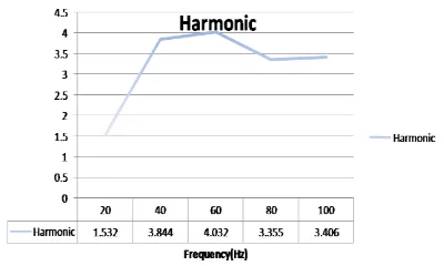
This paper address a low power, high speed class AB buffer amplifier topology for liquid crystal display applications which offer a rail to rail common mode input range. The presented circuit use two comparator circuit inside it to enhance the slewing capabilities with a limited power consumption and it draw a very small quiescent current during static operation for rail to rail common mode input range. The circuit describes here the capacitive load behaviour with reduced distortion at the output node for swing characteristics. By applying MTCMOS (Multi threshold CMOS) reduction technique leakage current is reduced from 56nA to 52nA, power is reduced from 377.3 pW to 221pW, reduced slew rate and tranconductance of 4.363. A buffer circuit can run 1nF of load capacitance of achieving a rise time 800E-12, duty cycle is 4.5, Average group delay is 221E-3, unity gain frequency is 221.7E-3 and harmonic frequency is 1.532 at 20 Hz. The circuit has been demonstrated at 45 nm technology.
Keywords
Amplifier, Buffer circuit, Driver circuit, Settling time, Slew rate.
1.
INTRODUCTION
A buffer amplifier circuit suggests a new compact reduced low power rail to rail configuration for large size LCD (Liquid crystal display) applications[1-2]. The proposed buffer circuit provides a phenomenal power efficiency improvement as comparison to the other reported solution [3]. The train drives of an LCD driving system contain the most significant role in achieving fast speed capabilities, high resolution and low power dissipation as well as the output buffer amplifiers essentially diagnose the speed, resolution, voltage swing and power consumption of the buffer amplifier circuit[4-5]. There are so many design challenges for the output buffer of an of an LCD (Liquid crystal display) driver [6]. The number of outputs to be achieved by using several column drivers of the buffer amplifier, so it should be used to minimize the system costs and increase the reliability of the circuit [7-8]. A flat panel display column driver three special requirements for the output buffer are to be needed. First a large number of output buffers are needed for a pixels column panel [9]. However it reduced the system cost and increases the reliability of the system. Second requirement is low power dissipation for the liquid crystal display (LCD) are commonly used in portable system that are battery powered [10-11].rd requirement is the input is always the step function of the output because the pixels are updated row by row [12]. Thus the power dissipation of the column driver is dependent on the image display [13]. In this paper we apply a reduction technique on the proposed circuit to reduced the size and getting a better power efficiency [14-15]. A variable bias current was used to reduce the power dissipation. However it wastes dynamic power when the grey level in a column driver does not
change. Due to the finite response time of the comparator circuit final voltage is always smaller then the input voltage. Multi threshold CMOS (MTCMOS) is a variation of CMOS chip technology which has transistors with multiple threshold voltages (Vth) in order to optimize delay or power [16]. The
Vth of a MOSFET is the gate voltage where an inversion layer
forms at the interface between the insulating layer (oxide) and the substrate (body) of the transistor. A common implementation of MTCMOS for reducing power makes use of sleep transistors. Logic is supplied by virtual power rail. Low Vth is used for fast switching speed and high Vth devices
connecting the power rail and virtual power rails are turned on in active mode, off in sleep mode. High Vth devices are used
as sleep transistors to reduce static leakage power.
2.
PROPOSED CIRCUIT AND
OPEREATION
2.1
Block Diagram
Figure Show the block diagram of the proposed two stage class AB buffer amplifier where C1and C2 are the current comparator which provide rail to rail input and output. MO1 and MO2 are the output complementary devices represent the series resistors are mainly used for phase compensation at the output node. The load capacitance is also connected to the output which is most portably used for swing characteristics of the output.
[image:1.595.320.534.490.623.2]. Fig.1:Block diagram of buffer amplifier
The basic comparator circuit are used to swing the output at the lightest difference between its inputs but there are many variations where the output is designed to switch between two other voltage values also. The input may be customized to make compares to an input voltage other then zero. The added comparators are used to reduce the power dissipation
2.2
Circuit Diagram
In the given circuit is connected to the inverting terminal
MO1 to Mo2 represent a push pull output gain stages. Rc is series resistance are used to show the connection between amplifier output and the load capacitor. Finally the buffer amplifier is capable of driving a wide range of load capacitance; phase compensation is performed by introducing a left half plane zero, which is produced by the load capacitance . The circuit consist of a comparator circuit which has been imposed in the buffer amplifier circuit for good swing characteristics having stronger current delivery for enhanced driving capability along with auxiliary transistors is apply to obtain the better driving of output without any distortion.
The transistor level enactment of the proposed output buffer is illustrated in fig.
Fig.2:Circuit schematic of the proposed two stage rail to rail buffer amplifier
The current buffers are mainly use frequency compensation technique. In current buffer amplifier the most popular common gate or cascode transistor topology used as a positive current buffer. The basic configuration scheme of the buffer amplifier with zero compensation technique is shown below
Fig.3:Buffer amplifier with zero compensation technique
To connect a capacitor across a high gain stage is the most significant compensation technique to improve the stability of the closed loop circuit. However to connect the capacitor in the output stage, a right half plane (RHP) zero is also created. The most commonly used method is dominant pole compensation which is also called as lag compensation. In open loop response pole is placed at an appropriate low frequency to reduce the gain of the amplifier to one (0db) for a frequency at or just below the location of the next highest frequency pole. This result the difference between open loop output phase and the phase response of a feedback network having no reactive elements never fall below -180o while the amplifier has a gain of one or more , ensuring stability.
3.
SIMPLIFIED IDENTICAL CIRCUIT
REPRESENTATION
OF
THE
PROPOSED
OUTPUT
DRIVING
BUFFER
The simplified identical circuit of the proposed output buffer is depicted in fig.
Fig.4:Simplified equivalent circuit of the proposed output driving buffer
Where gm1 and gm2 are the small signal tranconductance of the rail to rail stacked mirror differential amplifier and push pull output gain stages and Ro1and Ro2 represent the equivalent output resistances, Co1 and Co2 represent the output capacitances, whereas Rc represent the compensation
resistor and CL represent the equivalent capacitance of the
LCD panel.
Assuming Ro1, Ro2 >> Rc and Co1, Co2 << yields the following equations
(S) =
(1)
Where Ao is the DC open loop gain is expressed by
= (2)
While , and are the frequencies of the three
amplifier real poles
=
≈ (3)
(4)
≈ (5)
And is the frequency of the left-plane zero.
(6)
Here we represent Wp3 is the third pole frequency; however the equivalent circuit has contain three poles, and its contribution to the amplifier transfer function is negligible. When we increase the value of Rc and CL the phase margin is automatically increases.
4.
DESIGN ASPECTS AND OPERATING
PRINCIPAL
The differential pair circuit are designed to draw the static current value ɳIb, where Ib is the quiescent current which is supplied by the biasing network. The following relation is given below
ɳ
(7)
(8)
(9)
In quiescent state, no input signal is applied, current flowing in both input pair transistor are ɳIb/2. Assuming M5-M6 and M9-M10 are the current mirror image, While M7 and M11, draw the same static current ɳIb, In the output NMOS device MO2 would be pulled down towards Vss. In PMOS device MO1 would pulled up towards Vdd. So we can say that at DC characteristics it consume no static power.
(10)
(11)
If △V is sufficiently large then we get the following expression
ɳ
(12)
(13)
(14)
If the negative input step △V| is sufficiently large to get
ɳ
(15)
The power dissipated in the amplifier is of three types. The static power dissipation due to the dc bias current from the power supply of each transistor. The dynamic power dissipation due to the charging and discharging of the load capacitance and the direct path dissipation due to the current going through PMOS and NMOS transistor during transition.
The static energy dissipation for this circuit during a scanning period is expressed as
(16)
Where Ibias is dc bias current, fscanning is the scanning frequency. So we can say that amplifier always consume static dissipation.
For dynamic power dissipation is expressed as
= (17)
The energy dissipated in PMOS is as
= (18)
And then the pdischarge is as
= - (19)
= (20)
5.
MTCMOS TECHNIQUE
In MTCMOS technique, transistor of low threshold voltage becomes disconnected from power supply by using threshold sleep transistor on the top and bottom of the logic circuit. Transistor having low threshold voltage is used to design logic as shown in fig. The sleep transistors are controlled by the sleep signal. During the active, the sleep signal is disserted, causing both Vt transistor to turn on and provide a virtual power and ground to the low Vt logic.
When the circuit is inactive sleep signal is asserted forcing both high Vt transistor to cut off and disconnect power lines from the low Vt logic. This result a very low sub threshold leakage current power to ground when the circuit is in standby mode. One drawback of this method is that portioning and sizing of sleep transistor is difficult for large circuits.
Fig.5:The proposed MTCMOS structure
6.
NOISE, PHASE NOISE AND POLE
ZERO ANALYSIS
The graphical presentation of noise (db), phase noise (dbc) and pole zero (db) versus frequency (Hz) is shown given below
Fig.6: Parametric analysis of buffer amplifier with respect to frequency
Fig.7:Harmonic analysis of buffer amplifier with respect to frequency
7.
MODELLING AND SIMULATION
Figure8. show the reduced leakage current value by using MTCMOS (Multi threshold CMOS) reduction technique in which the value of reduced peak leakage current is 55.96nA is shown in given below at 45 nm technology by cadence virtuoso tool.
Fig.8:Reduced leakage current waveform using MTCMOS technique
Figure9. show the reduced power of peak value is 371.5pW by using MTCMOS(Multi threshold CMOS) technique to consume power for the maximum output at 45 nm technology is shown below by using cadence virtuso tool
Fig.9:Active power waveform using MTCMOS technique
Figure10. Show the value of slew rate by using MTCMOS (Multi threshold CMOS) technique having the maximum peak value of 15.81nS is shown in given below at 45 nm technology by using cadence virtuoso tool.
Fig.10:Slew rate analysis using MTCMOS technique
Figure11. Show the value of tranconductance by using MTCMOS (Multi threshold CMOS) technique having a value
of 4.363×10⁻¹² is given below at 45 nm technology by using cadence virtuoso tool.
Fig.11:Waveform of tranconductance using MTCMOS technique
Figure12. Show the noise response curve having a value of 5.202db by using MTCMOS (Multi threshold CMOS) technique is shown below at 45 nm technology by using cadence virtuoso tool
Fig.12:Noise response curve using MTCMOS technique
Figure13. Show the response curve of phase noise having a value of 52.75dbc/Hz by using MTCMOS (Multi threshold CMOS) technique at 45 nm technology by using cadence virtuoso tool.
Fig.13:Phase noise response curve using MTCMOS technique
Figure14. Show the pole zero response curve of having a value of -55.5db by using MTCMOS (Multi threshold CMOS) technique in the circuit at 45 nm technology by using cadence virtuoso tool.
Fig. 14:Pole zero responsecurve using MTCMOS technique
8.
TABLE
[image:4.595.318.537.96.170.2]S.N. PARAMETERS CONVENTIONAL MTCMOS
01 Power (pW) 375.6 371.5
02 Slew rate (V/µ
sec.)
15.81 15.41
03 Tranconductance
(µs/µm)
9.83 4.51
04 Leakage current
(nA)
56.66 55.96
Table1:CONVENTIONAL Vs MTCMOS
9.
CONCLUSION
In this paper, we have observed a low power consumption, high speed, large output swing, high performance and offer a rail to rail common mode input range. The comparator circuit are added in this circuit for enhancing the driving capability of the rail to rail CMOS buffer amplifier in which it sense the rise and fall time of the input waveform and it consume the power dissipation. By using a reduction technique MTCMOS (multi threshold CMOS technique) reduced parameters are obtained. We observed noise 5.202, phase noise 52.75dbc/Hz and pole zero 55.57db at 45 nm technology. The proposed output buffer circuit is suitable for the application of flat panel display.
10.
ACKNOWLEDGEMENT
The authors would like to thank ITM Universe, Gwalior in collaboration with Cadence system design, Bangalore.
11.
REFRENCES
[1] David JR Cristaldi, Salvatore Pennisi, Francesco Pulvirenti, Liquid Crystal Display Drivers: Techniques and Circuits. New York: Springer, Mar. 2009, vol.14, pp. 397-400.
[2] S. Di Fazio, S. Pennisi, F. Pulvirenti, and T. Signorelli, “670-nACMOSOTA for AMLCD column driver,” J. Circuits, Syst., Comput., vol. 18, no. 2, pp. 339–350, Apr. 2009
[3] J.-H. Wang, J.-C. Qiu, H.-Y. Zheng, C.-H. Tsai, C.-Y. Wang, C.-C.Lee, and C.-T. Chang, “A compact low-power high slew-rate rail-torailclass-AB buffer amplifier for LCD driver ICs,” in Proc. EDSS ’07, Dec. 2007, vol.3,pp. 397–400.
[4] Y. S. Son, J. H. Kim, H. H. Cho, J. P. Hong, J. H. Na, D. S. Kim, D.K. Han, J. C. Hong, Y. J. Jeon, and G. H. Cho, “A column driver with low-power area-efficient push-pull buffer amplifiers for active-matrix LCDs,” ISSCC Dig. Tech. Papers, vol.7, pp. 142–143, Feb. 2007.
[5] C.-W. Lu and P. H. Xiao, “A high-speed low-power rail-to-rail buffer amplifier for LCD application,” in Proc. CCECE ’06, Dec. 2006, vol.6, pp.709–712.
[6] R. Mita, G. Palumbo, and S. Pennisi, “Low-voltage high-drive CMOS current feedback op amp,” IEEE Trans. Circuits Syst. II, vol. 52, pp.317–321, June 2005 [7] M. Annese, S. Bertaiola, G. Croce, A. Milani, R.
Roggero, P. Galbiati,and C. Costiero, “0.18 BCD-High Voltage Gate (HVG) process to address advanced display drivers roadmap,” Proc. Power Semiconductor Devices and ICs, vol.6, pp. 363–366, 2005
[8] T. Itakura, H. Minamizaki, T. Satio, and T. Kuroda, “A 402-outputTFT-LCD driver IC with power control based on the number of colors selected,” IEEE J. Solid-State Circuits, vol. 38, no. 3, pp. 503–510,Mar. 2003
[9] C.-W. Lu and C. L. Lee, “A low-power high-speed class-AB buffer amplifier for flat-panel-display application,” IEEE Trans. Very Large-Scale Integr. (VLSI) Syst., vol. 10, no. 4, pp. 163–168, Apr. 2002.
[10]M.-C. Weng and J.-C. Wu, “A compact low-power rail-to-rail class-B buffer for LCD column driver,” IEICE Trans. Electron., vol. E85-C, no.8, pp. 1659–1663, Aug. 2002.
[11]T. Itakura, “A high slew-rate operational amplifier for an LCD driver IC,” IEICE Trans. Fundamentals, vol. E78-A, no. 2, pp. 191–195, Feb.1995
[12]C.-C. Wang, J.-C. Wu and C.-M. Huang, “Data line driver design for a 1000 480 _ 640 _ 3 color FED,” in Proc. 9th Int. Vacuum Microelectronics Conf., St. Petersburg, FL, July 1996, pp. 557–561.[3] Hitachi Corp., Hitachi LCD Controller/Driver LSI, 1993.
[13]C.-C. Wang, J.-C. Wu and C.-M. Huang, “Data line driver design fora 10² 480 _ 460 _ 3 color FED,” in Proc. 9th Int. Vacuum Micro electronics Conf., St. Petersburg, FL, July 1996, pp. 557–561
[14]H. Khorramabadi, “A CMOS line driver with 80 dB linearity for ISDN applications,” in 1991 Symp. VLSI Circuits Dig. Tech. Papers, June 1991,pp. 75–76. [15]H. Khorramabadi, “A CMOS line driver with 80 dB
linearity for ISDN application,” in Proc. 1991 Symp. VLSI Circuits Dig. Tech. Papers, June1991, pp. 75–76. [16] H. Parzhuber and W. Steinhagen, “An adaptive biasing
one-stage CMOS operational amplifier for driving high capacitive loads,” IEEE J. Solid-State Circuit, vol. 26, pp. 1457–1460, Oct. 1991
[17]Y. Takahashi et al., “Multimedia projector using 720 _ 480 pixel a-Si TFT-LCD’s and a high-speed analogue driver LSI,” Displays: Technology& Application, vol. 13, no. 1, pp. 5–30, Jan. 1992
[18]P.-C. Yu and J.-C. Wu, “A Class-B output buffer for flat-panel-display column driver,” IEEE J. Solid-State Circuits, vol. 34, pp. 116–119, Jan.1999.
[20]E. R. Nowak, M. B. Weissman, and S. S. P. Parkin, “Electrical noise in hysteretic ferromagnet-insulator-ferromagnet tunnel junctions,” Appl.Phys. Lett., vol. 74, pp. 600–602, 1999.
[21]M. Scaffardi, P. Ghelfi, E. Lazzeri, L. Potì, and A. Bogoni, “Photonic processing for digital comparison and full addition based on semiconductor optical amplifiers,” IEEE J. Sel. Topics Quantum Electron., vol.14, no. 3, pp. 826–833, May 2008
[22]G. Berrettini, G. Meloni, L. Potì, and A. Bogoni, “Variable optical buffer for packet storage in OPS nodes,” in Proc. SPIE Photonics Eur.’10 Int. Conf., Brussels, Belgium, Apr. 2010.
[23]C. Fager, L. Landen, and H. Zirath, “High output power, broadband28–56 GHz MMIC frequency doubler,” in IEEE MTT-S Int. Dig., Jun.2000, vol. 3, pp. 1589–1591. [24]M. Ferndahl, B. M. Motlagh, and H. Zirath, “40 and 60
GHz frequency doublers in 90-nm CMOS,” in IEEE MTT-S Int. Dig., Jun. 2004, pp.179–182.