http://www.scirp.org/journal/jemaa ISSN Online: 1942-0749
ISSN Print: 1942-0730
New Formulation of the Mulilayer
Iterative Method: Application to
Coplanar Lines with Thick Conductor
Rafika Mejri, Taoufik Aguili
Communication System Laboratory Sys’Com, National Engineering School of Tunis, University of Tunis El Manar, Tunis, Tunisia
Abstract
The skin effect is an electromagnetic phenomenon that makes the current flows only on the surface of the conductors at high frequency. This article is based on the phe-nomenon to model a structure made in coplanar technology. In reality, these types of structures integrated metal layers of different thickness of copper (9 μm, 18 μm, 35 μm, 70 μm). The neglect of this parameter introduces errors, sometimes significant, in the numerical calculations. This is why an iterative method (FWCIP) based on the wave concept was restated. Validation of results was carried out by comparison with those calculated by Ansoft HFSS software and Agilent ADS Technology. They show a good matching.
Keywords
Skin Effect, Electromagnetic Phenomenon, Iterative Method, Coplanar Structure, Microwave
1. Introduction
In Radio frequency, most devices are made in micro strip technology [1] [2]. This technology became the best known and most used. This is due to its flat nature, ease of manufacturing, low cost, easy integration with circuits in the solid state, good heat dis-sipation structure that is used as good mechanical support etc. In general and in various research works concerning modeling and study of these structures, most researchers assumed that they possessed metallic conductors without thickness [3] [4]. This sim-plifying assumption decreases the accuracy of the results of analytical methods used for the characterization of these structures. Several methods were used to characterize the influence of the thickness of the conductor used, such as mode-matching method [5], How to cite this paper: Mejri, R. and Aguili,
T. (2016) New Formulation of the Mulilayer Iterative Method: Application to Coplanar Lines with Thick Conductor. Journal of Elec-tromagnetic Analysis and Applications, 8, 197- 218.
http://dx.doi.org/10.4236/jemaa.2016.89019
Received: July 10, 2016 Accepted: September 27, 2016 Published: September 30, 2016
Copyright © 2016 by authors and Scientific Research Publishing Inc. This work is licensed under the Creative Commons Attribution International License (CC BY 4.0).
method of lines [6], spectral domain method [7] and conformal mapping method [8]. For the study of structures with flat and thick conductors such as micro strip line in this document, we have taken the first model proposed in [6]. A new formulation of the iterative method FWCIP (Fast Wave Concept Iterative Process) was made to extend the study of planar structures with thick flat conductor. This method is based on the con-cept of wave [9]. It is developed for the simple planar layer modeling of structures [10]
or multi-layer [11], and even arbitrarily complex shape. This is an easy method to im-plement due to the absence of test functions. It is always convergent and has considera-ble execution speed due to the FMT (Fast Modal Transform).
2. Iterative Method FWCIP
This method is well suited to the calculation of planar structures. In fact, TE and TM modes are used in the iterative method as digital basis of spectral domain in which the FFT. Subsequently, the concept of fast wave is introduced to reflect the boundary con-ditions and continuity of relationships in different parts of the interface Ω in terms of waves.
The method involves determining an effective relationship to link the incident and reflected waves in different dielectric layers expressing thoughts in modal domain and the boundary conditions and continuity, expressed in terms of waves in spatial domain. The iterative process is then used to move from one field to another using the FMT thus accelerating the iterative process and then the convergence of the method. The use of the FMT requires the pixel description of the different regions of the dielectric inter-faces. Thus the electromagnetic behavior of a planar structure will be described by writing the boundary conditions and continuity of the tangential fields on each pixel containing the interface circuitry to study. This integral formulation retains the advan-tages well known iterative methods including ease of implementation and speed of ex-ecution.
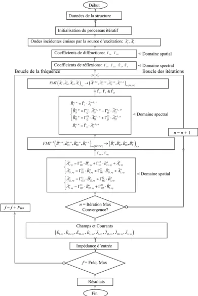
The flowchart in Figure 1 summarizes the evolution of the iterative method for a planar structure with three layers of different mediums [12].
The theoretical formulation for the iterative method is based on determining the re-lationship between the incident waves A1
, A21
, A22
and A3
defined in spatial do-main and the reflected waves B1
, B21
, B22
and B3
, defined in the spectral domain. The passage of the spatial domain to the spectral domain is using modal Fourier trans-form (FMT). The passage of the spectral domain to the space domain is using the transform inverse Fourier modal (FMT − 1). These operations are done with repeti-tions until the convergence of the method. FMT and FMT − 1 are used to speed up the computation time of the method.
1
ˆΩ
Γ and ΓˆΩ2: Diffraction operators, giving the incident waves from the reflected
waves that diffract at the discontinuities plans (Ω1 and Ω2). They are defined in spatial
domain and found in these image operators circuits placed at plans (Ω1 and Ω2).
ˆ
k
Γ : Operator reflection ensuring the link between the incident waves and the
ing walls and the relative permittivity of the different mediums of the structure, k ∈ {medium1, medium 3}.
ˆ
Q
Γ : Diffraction Operator at each interface (Ω1 and Ω2).
The evolution of iterations through the spectral domain to the space domain is done using the Fourier transform modal “FMT” which considerably reduces the calculation time. Modal Fourier transform requires the fragmentation of discontinuity planes (Ω1
and Ω2) in pixels and this so that the electromagnetic behavior of the overall circuit will
be summarized by writing the boundary conditions and continuity of the tangential fields on each pixel. The iterative process stops when it reaches the convergence of re-sults.
The terms below link the incident waves “A1
, A21
, A22
and A3
” to the reflected waves “B1
, B21
, B22
and B3
” when they pass the space domain to the spectral do-main:
0
1 1 1
1 0
21 21 2
21 21 22 22 22 22 2 3 3 11 12 21 21
22 21 22 22
ˆ ˆ ˆ ˆ ˆ ˆ ˆ Q
A B A
A B A
B A B A A B A B Y Y J E
J Y Y E
Ω
Ω
= Γ +
= Γ = Γ = (1)
The operators of diffraction ΓˆΩ1 and ΓˆΩ2 contains the images of circuit that being in the Ω1 and Ω2 plans.
Diffraction Operator: ΓˆΩ1
For a source of bilateral excitation polarized in (oy), the overall diffraction operator is written from the diffraction operators in different regions of Ω1 plane (metal region,
source region of excitement, dielectric region):
(
)
(
)
(
)
(
)
x 1 y01 02 0 01 02 02 01 0 01 02 01 02
1 1 1 1
01 02 0 01 02 01 02 01 02 0 01 02 01 02
0 01 02 01 02
1
01 02 0 01 02 01
ˆ
2 2
ˆ ˆ ˆ ˆ ˆ
2 ˆ 2
m S i S i
S
Z Z Z Z Z Z Z Z Z Z Z Z
H H H H H
Z Z Z Z Z Z Z Z Z Z Z Z Z Z
Z Z Z Z Z
H
Z Z Z Z Z Z
Ω
Γ
+ − − − − ⋅ + ⋅ ⋅ + ⋅ + + + + + + = ⋅ + + + +
(
)
(
)
01 02 0 01 02 01 02
1 1 1 1
02 01 02 0 01 02 01 02
ˆ ˆ ˆ ˆ
i m S i
Z Z Z Z Z Z Z
H H H H
Z Z Z Z Z Z Z Z
− − − ⋅ − − ⋅ + ⋅ + + + (2)
where: Hs1 = 1 on the source and 0 elsewhere.
Hm1 = 1 on the metal and 0 elsewhere.
Hi1 = 1 on the dielectric and 0 elsewhere.
Diffraction Operator: ΓˆΩ2
03 02 02 01
2 2 2
03 02 03 02
x 2
y 03 02 03 02
2 2 2
03 02 03 02
2
ˆ ˆ ˆ
ˆ
2 ˆ ˆ ˆ
m i i
i m i
Z Z
Z Z
H H H
Z Z Z Z
Z Z Z Z
H H H
Z Z Z Z
Ω
−
− + ⋅ ⋅
+ +
Γ =
−
⋅ − + ⋅
+ +
(3)
where: Hm2 = 1 on the metal and 0 elsewhere.
Hi2 = 1 on the dielectric and 0 elsewhere
Expression of the reflection operator: ˆ
k
Γ
It is defined in the spectral domain and contains information about the nature of the housing and the relative permittivity of the medium 1 and 3 of the structure. It is ex-pressed by the following relationship:
, 0
,
, , 0
1 ˆ
1
k k mn
k mn k mn
m n k mn
Z Y f f Z Y α α α α α − Γ = +
∑
(4)mn
fα : Basic functions. It depends on the nature of the box.
0 k k r Z η ε
= : Impedance of the middle k ∈ {midium1, medium 2}.
120
η
= Π: Vacuum impedance.,k mn
Yα : Mode admittance reduced to the level of Ω plan.
-For a top cover (or lower) placed at a distance h from Ω plan.
( )
(
( )
)
,
coth
k k
k
mn mn r mn r
Yα =Yα ε ⋅ γ ε ⋅h (5)
-For An open circuit without top cover (or lower).
( )
,k
k
mn mn r
Yα =Yα ε (6)
( )
kmn r
Yα ε : Mode admittance expressed by:
( )
( )
( )
( )
0 0 : : k k k k k mn r TE mn r r TM mn r mn r TE Y j j TM Y γ ε ε ωµ ωε ε ε γ ε = = (7)( )
kmn r
γ ε : Propagation constant
( )
2 22 2
0
k k
mn r r
m n
k
a b
γ ε = Π + Π − ε
(8)
0
k c ω
= : Wave number in a vacuum.
0 0
1 c
ε µ
= : Speed of light (3 × 10⁸ m/s)
m, n: Designating the index for modes∈ {N}.
α: mode indicator TE (Transverse Electric), TM (Transverse Magnetic).
k: Medium considered k ∈ {1, 2}.
k r
0
ε : Vacuum permittivity (F/m).
µ0: Magnetic vacuum permeability (H/m).
ω: Angular pulsation equal to pulsation 2∏f (rd/s). Expression of the FMT
The Fourier transform in cosine and sine is defined by:
( )
( )
( )
( )
01 02 01 021 1 01 02
cos sin
1 1 01 02
, cos sin
, 2
,
, sin cos
N N x i j x N N y y i j
m i n j
E i j
N N
E i j
D FFT
E i j m i n j
E i j
N N
= = = =
⋅ Π ⋅ Π
− =
Π Π
⋅ ⋅
∑∑
∑∑
(9)The Fourier mode transform (FMT) is defined by:
( )
( )
( )
( )
cos sin
, ,
ˆ 2 FMT
, , TE x x mn TM y y mn
E i j E i j
e
T D FFT
E i j E i j
e
= ⋅ − =
(10)
ˆ
T: Passing modal operator in the area expressed by:
(
)
ˆ ,
n m
b a
T K m n
m n a b − = ⋅ (11)
(
)
2 2 2 1 , mnK m n
ab m n a b σ = ⋅ + (12)
The reflection operator of the Quadruple: ˆ
Q
Γ
The reflection operator of the Quadruple is defined in layer 2 of the structure to be studied. It links the incident waves “A21
, A22
” the reflected waves “B21
, B22
” they pass the space domain to the spectral domain. The quadruple Q ensures the passage of plan Ω1 to plan Ω2 and inversely.
According to the diagram in Figure 1 we can write:
21 21 22 22 ˆ Q B A B A
= Γ
(13) Parameters ˆ
ij
Y du quadruple Q:
21 11 21 12 22
22 21 21 22 22
J Y E Y E
J Y E Y E
= +
= +
(14)
0 1 21
2 22 3
1 3
1 21
22 3 h
J J J
J J J
J Y E
E E E E = + = + = = = (15)
11 22 12 21 ˆ ˆ ˆ ˆ Y Y Y Y = =
After some mathematically manipulation, it is possible to determine the matrix:
(
) (
)
(
) (
)
2 2
11 02 12 02 12 02
2 2
12 02 11 02 12 02
1 2
1 ˆ
2 1
Q
Y Z Y Z Y Z
C Y Z Y Z Y Z
− + −
Γ =
− − +
(16)
With:
(
) (
2)
211 02 12 02
1
C= +Y Z − Y Z
(
) (
)
(
) (
)
(
) (
)
(
) (
)
(
) (
)
(
) (
)
2 211 02 12 02 12 02
2 2 2 2
11 02 12 02 11 02 12 02
2 2
, ,
11 02 12 02
12 02
2 2 2 2
11 02 12 02 11 02 12 02
1 2
1 1
1 2
1 1
mn mn mn mn
Q m n
mn mn mn mn
Y Z Y Z Y Z
f f f f
Y Z Y Z Y Z Y Z
Y Z Y Z
Y Z
f f f f
Y Z Y Z Y Z Y Z
α α α α
α α α α α
− + −
+ − + −
Γ =
− + − + − + −
∑
(17)(
) (
)
(
) (
)
(
) (
)
(
) (
)
(
) (
)
2 2
11 02 12 02 12 02
21 2 2 21 2 2 22
, , 11 02 12 02 , , 11 02 12 02
2 2
11 02 12 02 12 02
22 2 2 21
, , 11 02 12 02
1 2
1 1
1 2
1 1
mn mn mn mn
m n m n
mn mn mn
m n
Y Z Y Z Y Z
B f f A f f A
Y Z Y Z Y Z Y Z
Y Z Y Z
Y Z
B f f A f
Y Z Y Z
α α
α α α α α α α
α α
α
α α α α α
α − + − = + + − + − − − + = + + − +
∑
∑
∑
(
) (
2)
2 21, , 11 02 12 02
mn m n
f A
Y Z Y Z
α α α α −
∑
(18) mnfα : Bases function of the box modes.
With α ∈
{
TE TM,}
.3. Formulation of the Problem
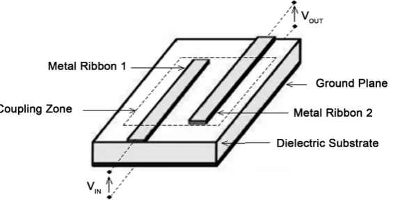
[image:7.595.235.518.541.685.2]To show the robustness of this new formulation of the iterative method we have applied to the study of two coupled micro strip lines, parallel, symmetrical and placed in the same plane. Metal foils which constitute them are copper and have a thickness which is important. The structure of these is presented below in Figure 1 and Figure 2. This structure is the basic element of a band-pass filter or band cut made in coplanar tech-nology. This filtering function can be encountered in all the wireless emission-receiving systems.
In our model both input and output voltage “VIN et VOUT” of the structure to study will be modeled by two field sources S1 {E1, J1} and S2 {E2, J2}.
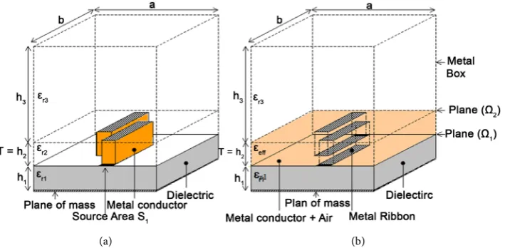
3.1. Electromagnetic Model of the Study Structure
Figure 3(a) shows the structure to study and Figure 3(b) shows the electromagnetic model we propose to study this structure. The latter consists in three layers of different materials. The first layer is filled with a dielectric substrate, assumed without loss, rela-tive permittivity εr1 and thickness h1. It is placed between the ground plane and the plane Ω1 discontinuity. The second layer thickness h2 of which is equal to the thickness
T of the formants metal strips the two coplanar lines. It is placed between the two plans of Ω1 and Ω2 discontinuities and consisting of a complex effective permittivity εeff
medium modeling the different materials (copper and Air) formants this medium. The third layer is filled with air. It is placed between the Ω2 discontinuity plane and the top
cover of the metal housing which surrounds the entire structure. The use of a metal case is necessary for reasons of shielding and modeling.
Structural parameters: a=4.754 mm , b=4.754 mm , c1≈0.26 mm ,
1 0.037 mm
d ≈ , s≈0.074 mm , L≈3.53 mm , h1=0.254 mm , h2 = =T 10 mµ , 3 1.99 mm
h = , ε =r1 9.9, εr2=εeff , ε =r3 1,
6
59.6 10 S m
σ = × .
The plan of discontinuity Ω1 contains the input and the output of the circuit and the
two metal ribbons, without thickness, modeling the undersides of the two micro strip lines. The Ω2 plan only contains two metal ribbons, without thickness, modeling the
upper faces of the two micro strip lines (Figure 4 and Figure 5).
3.2. Technical Calculation
Y
ijParameters of the Coupling Matrix
between the Sources of Excitations
S1
(
E1
,
J1
) and
S2
(
E2
,
J2
).
We present in Figure 6 the technique for calculating admittances Yij parameters of the
coupling matrix between the different sources of excitations of the study structure. This technique allows the electromagnetic calculation of equivalent quadruple source view of
[image:8.595.199.554.512.686.2](a) (b) Figure 4. Quotes of discontinuities plans. (a): Plan Ω1; (b): Plan Ω2.
[image:9.595.198.552.486.676.2](a) (b)
Figure 5. Definition of the different regions of the discontinuities plans (a): Plan Ω1; (b): Plan Ω2.
Figure 6. Technical way of calculating Yij admittances parameters of the coupling matrix between S1 (E1, J1) et S2 (E2, J2).
y
x d1
d1
c1
c1
s
L L
o
a b
y
x d1
d1
c1
c1
s
L L
o
a b
(Hs1)
Région Source S1
Région Diélectrique
(Hi1)
Région Métallique (Hm1) Région
Source S2
(Hs2) Région Métallique
(Hm2)
(Hi2)
excitations considered S1 (E1, J1) et S2 (E2, J2). In this technique we apply the superposi-
tion theorem that considers the study structure is alternately excited by the source S1
(E1, J1) then by the source S2 (E2, J2). This brings us to a problem with a single excitation
source whose theoretical development is simple to prepare.
The study of structure (Figure 7(a)) is energized by two sources localized S1 (E1, J1)
and S2 (E2, J2). This sets the quadruple coupling shown in Figure 7(b).
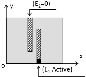
1st Step: The localized source S1(E1, J1) is activated.
In this step we short circuit the excitation source n˚2 (E2 = 0), as shown in Figure 8
we calculate input admittance seen by the excitation source n˚1 “Y11” and the transfer
admittance (or coupling) of the n˚1 source to the source n˚2 “Y21”.
The matrix representation (1) allows us to write:
1 11 1 12 2
2 21 1 22 2
J Y E Y E
J Y E Y E
= +
= +
(1)
1
1 11 1 11
1 2
2
2 21 2 21
2
0
J
J Y E Y
E E
J
J Y E Y
E
= ⇒ =
= ⇒
= ⇒ =
(2)
J1 and J2 current densities are created by the excitation source {S1} respectively at the
source {S1} and location of the source shorted {S2}. So that the parameters Y11 and Y21
[image:10.595.195.554.394.510.2](a) (b)
[image:10.595.300.443.559.687.2]Figure 7. (a) Study Structure excited by two sources {S1 et S2}; (b) Coupling quadrupole between enter {S1 et S2}.
Figure 8. Study Structure excited by the source {S1}.
(E
1Active)
(E
2=0)
x
y
are respectively the admittance seen by excitation source {S1} and the admittance
view-points occupied by the source shorted {S2}.
2nd Step: The localized source S2(E2, J2) is activated
In this second step we short-circuit the source n˚1 (E1 = 0), as shown in Figure 9 we
calculate the input admittance seen by the excitation source n˚2 “Y22” and the transfer
admittance (or coupling) from source 2 to source n˚1 “Y12”.
The matrix representation (1) allows us to write:
1 11 1 12 2
2 21 1 22 2
J Y E Y E
J Y E Y E
= +
= +
(3)
1
1 12 2 12
2 1
2
2 22 2 22
2
0
J
J Y E Y
E E
J
J Y E Y
E
= ⇒ =
= ⇒
= ⇒ =
(4)
J1 and J2 current densities are created by the excitation source {S2} respectively at
source level {S2} and the location of the source shorted {S1}. So that the parameters Y22
and Y12 are respectively the admittance seen by excitation source {S2} and the
admit-tance viewpoints occupied by the source shorted {S1}.
The calculation of parameters Yij coupling matrix requires a convergence study of
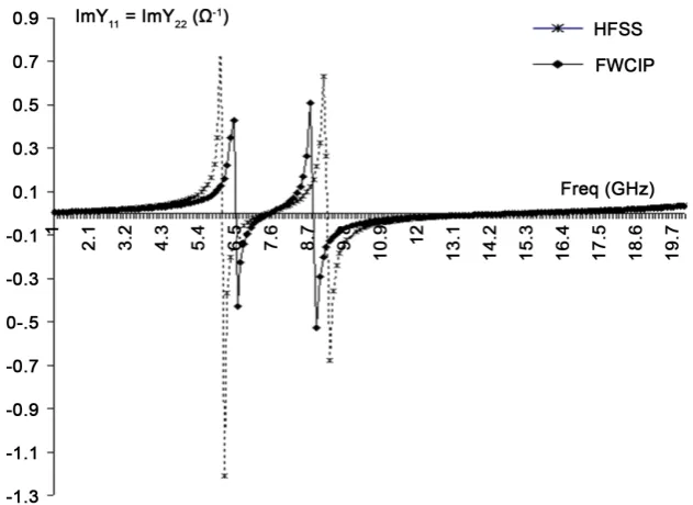
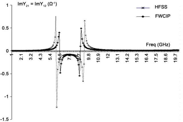
these items based on iterations, optimizing the computation time and increasing the accuracy of these results. By observing Figure 10 and Figure 11 we find that the num-ber of iterations required for convergence of admittances Y11, Y12, Y21 and Y22 is 4000
[image:11.595.327.463.180.271.2]iterations for a frequency f = 5 GHZ. This frequency is far from the resonance of the structure where we have maximum energy. At this level it takes a lot more iterations to reach convergence (about 20,000 iterations). Given the symmetry of the structure we find that: Y11 = Y22 and Y21 = Y12.
Figure 12 and Figure 13 respectively show changes depending on the frequency of the input admittance seen by the excitation source n˚1 “Y11” and the transfer
admit-tance (or coupling) of the source n˚1 to the source n˚2 “Y21”. The validation of these
results was carried out by comparison with those calculated by Ansoft HFSS software. This comparison shows that both results have the same variations and coincide with the 7.6 GHZ frequency. We notice a discrepancy between our results and those of HFSS software in the order of 4%.
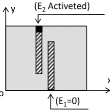
Figure 9. Studied structure excited by the source {S2}. (E2Activeted)
(E1=0)
x y
[image:11.595.316.429.575.687.2]Figure 10. Input admittance Y11 convergence based on iterations for (f = 5 GHZ).
Figure 11. Coupling admittance convergence Y21 based on iterations for (f = 5 GHZ).
Figure 13. Transfer admittance (or coupling) Y21 according to the frequency (number of itera-tions: 5000).
Admittances Y11 and Y22, are identical, this is translated by the symmetry of the
structure, same for the admittances Y12 and Y21.
3.3. Calculating
S
ijParameters of the Study Structure
The parameters Yij of the coupling matrix between the two circuit excitation sources
have been found. It remains to calculate the characteristic impedance of the study structure is necessary for the calculation of Sij parameters.
3.3.1. Calculation of Characteristic Impedance ZC of the Study Structure
We applied in a first step the empirical formulas of Hammerstad (based GARDIOL) to calculate the characteristic impedance of the study structure. These formulas we offer values approaching Zc. For more details on the characteristic impedance must use a
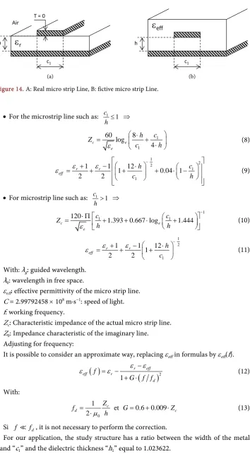
numerical method for the calculation.
εr is the relative permittivity of the dielectric which is the speeding of the
electro-magnetic wave. By cons in a microstrip line (Figure 14(a)), the speeding is done in two different environments εr “dielectric and the air”. To simplify the problem we must
de-termine an equivalent dielectric constant εeff (Figure 14(b)), this model based on εrand
h.
0 g
e
λ λ
ε
= (5)
0
C f
λ = (6)
0 c
e
Z Z
ε
(a) (b) Figure 14. A: Real micro strip Line, B: fictive micro strip Line.
•For the microstrip line such as: c1 1
h ≤ ⇒
1 1 60 8 log 4 c e e c h Z c h
ε
⋅ = + ⋅ (8)
1
2 2
1 1
1 1 12
1 0.04 1
2 2 r r eff c h c h ε ε ε − + − ⋅ = + + + ⋅ − (9)
•For microstrip line such as: c1 1
h > ⇒
1
1 1
120
1.393 0.667 log 1.444
c e e c c Z h h ε −
⋅ Π
= + + ⋅ +
(10)
1 2
1
1 1 12
1 2 2 r r eff h c ε ε ε − + − ⋅ = + +
(11) With: λg: guided wavelength.
λ0: wavelength in free space.
εeff: effective permittivity of the micro strip line.
C = 2.99792458 × 10⁸ m∙s−1: speed of light.
f: working frequency.
Zc: Characteristic impedance of the actual micro strip line.
Z0: Impedance characteristic of the imaginary line.
Adjusting for frequency:
It is possible to consider an approximate way, replacing εeff in formulas by εeff(f).
( )
(
)
21
r eff
eff r
d
f
G f f
ε
ε
ε
=ε
− −+ ⋅ (12)
With:
0
1
et 0.6 0.009 2
c
d c
Z
f G Z
h µ
= = + ⋅
⋅ (13)
Si f fd, it is not necessary to perform the correction.
For our application, the study structure has a ratio between the width of the metal band “c1” and the dielectric thickness “h1” equal to 1.023622.
T = 0 Air
c1
h
ε
effh
ε
r1 1
1.023622 1 C 48.25
c
Z
h = > ⇒ = Ω
The relative error obtained with respect to the characteristic impedance calculated using the ADS Linecalc tool (which is equal to 47,618 Ω) is equal to 1.3% This is for equal work often 13.5 GHZ.
3.3.2. Calculation of SijParameters of the Study Structure
The Yij parameters of the structure study were calculated and so does the characteristic
impedance Zc. This allows to deduce the Sij parameters of the two micro strip lines
cop-lanar relationship defined below:
(
)(
)
(
)(
)
2
11 22 12 21
11 2
11 22 12 21
1 1
1 1
c c c
c c c
Z Y Z Y Z Y Y
S
Z Y Z Y Z Y Y
− ⋅ + ⋅ + ⋅
=
+ ⋅ + ⋅ − ⋅ (14)
(
)(
21)
21 2
11 22 12 21
2
1 1
c
c c c
Z Y
S
Z Y Z Y Z Y Y
− ⋅ ⋅ =
+ ⋅ + ⋅ − ⋅ (15)
(
)(
)
(
)(
)
2
11 22 12 21
22 2
11 22 12 21
1 1
1 1
c c c
c c c
Z Y Z Y Z Y Y
S
Z Y Z Y Z Y Y
+ ⋅ − ⋅ + ⋅
=
+ ⋅ + ⋅ − ⋅ (16)
(
)(
12)
12 2
11 22 12 21
2
1 1
c
c c c
Z Y
S
Z Y Z Y Z Y Y
− ⋅ ⋅ =
+ ⋅ + ⋅ − ⋅ (17)
Calculating the parameters in decibel Sij is done by applying Equation (14) below:
( )
( )
2( )
210
dB 20 log Re Im
ij ij ij
S = ⋅ S + S (18)
We present in the following, the effect of the error obtained in the approximate cal-culation of the characteristic impedance of the parameters Sij.
Formulas Hammerstad:
11 21
48.25 1.959552 dB et 4.861236 dB
c
Z = Ω ⇒S = − S = −
LineCalc of ADS:
11 21
48.618 1.919848 dB et 4.935580 dB
c
Z = Ω ⇒S = − S = −
Error:
Error on Zc = 1.3%, Error on S11 = 2%, Error on S21 = 1.5%.
An error of 1.3% on the characteristic impedance results in an error of 2% on the coefficient of reflection S11 and an error of 1.5% on the transmission coefficient S21. This
[image:15.595.278.491.226.359.2]for equal work often 13.5 GHZ and 5000 iterations. We note that there is a slight in-crease of this error on the Sij parameters relative error on Zc.
Figure 15 and Figure 16 respectively show the variations in the transmission coeffi-cients “S21” and reflection “S11“ based on the frequency. Also view the symmetry of the
structure we have obtained “S11 = S22” and “S21 = S12”. These results noted a strong
coupling between the two sources of excitation in the frequency band “41.6 GHZ - 42 GHZ” where the coefficients of transmissions “S21 and S12” are strictly greater than −3
dB - 3 dB and reflection coefficients “S11 et S22” are strictly less than −10 dB. In this
Figure 15. Transmission coefficient as a function of the frequency (Number of iterations: 1000).
Figure 16. Reflection coefficient as a function of the frequency (Number of iterations: 1000).
By cons in the frequency band “22.4 GHZ - 28.8 GHZ” coupling is very small be-tween the two sources of excitations. In this frequency band the coefficients of trans-missions “S21 and S12” are strictly less than –10 dB “S11 and S22” and coefficients of
ref-lections are strictly greater than −1.2 dB. The circuit mismatched with the two inputs and it behaved like a notch filter.
We report in Figure 17 the variation of the according transmission coefficient of the thickness T of the metal strip. This for equal work often 13.5 GHZ and 5000 iterations. This curve shows that if we increase the thickness of the metal strips the transmission between the two sources of excitations increases, which is quite normal and valid even used the method of analysis. For a strictly smaller thickness 1µm we note that the varia-tion is very low and the metal ribbons behave like metal strips without thickness. The beginning of the answer starts from 1 µm and lasts up to 60 μm where we notice a marked increase in transmittance with the thickness T. while increasing beyond 60 μm, we notice a saturation which is due probably to the cancellation of the edge effect. We will have a planar waveguide behavior that is different from two thin lines. The energy propagation is thus made according to this waveguide which is well known and charac-terized by its propagation constant “β = ω/c” which is linear and its characteristic
im-pedance which is defined by:
0 0 C
Z
µ
ε
[image:17.595.275.472.347.498.2]= (18)
[image:17.595.275.470.539.677.2]Figure 18 shows the variation of the transmission coefficient as a function of the thickness T of the metal strip and as a function of frequency. This is for 5000 iterations.
Figure 17. Variation of the transmission coefficient “S21” based on the thickness T of the metal strip.
These curves show that if we increase the thickness of the metal strips the transmission between the two sources of excitations increases regardless of the operating frequency.
4. Effect of Housing on the Results of the Problem
We see in the results of 15 and 16 to a certain oscillation frequency 42.2 GHZ which is mainly due to the resonance of the housing. This oscillation is also observed in the re-sults given by HFSS and ADS software. In fact to justify this we proceed to demon-strate.
[image:18.595.238.508.274.440.2]We start with the ADS software. We compare the results of simulations of the struc-ture with and without housing Figure 19 and Figure 20 shows the results when we see that this oscillation appears only in the results of the structure with the presence of the housing and is located 42.8 GHZ frequency.
Figure 19. Coefficients of transmission and reflection versus frequency (without the presence of the housing).
[image:18.595.236.512.493.671.2]Figure 21 and Figure 22 show the resonance of the housing. They are derived from the difference of the results of the two curves of Figure 19 and Figure 20.
We are interested in our method of analysis. We take a metal housing walls that we excited by two sources of localized fields, but without the presence of micro-strip lines. We keep the same physical parameters of the study structure (Figure 23).
The different results obtained by simulation of the coefficients of reflection and transmission (Figure 24 and Figure 25), show the persistence of the resonance even in the absence of micro-strip lines, which confirms the presence of a resonance of the housing in the structure.
5. Conclusion
This article allowed us to review an electromagnetic model with what we have characte-rized as a planar structure including a flat, thick copper conductor. Indeed this model which is based on the phenomenon of skin effect encouraged us to model the latter two metal ribbons without thickness, placed one above the other which has a h2 distance
[image:19.595.207.539.352.690.2]equal to the thickness T of conductor. Both sides, parallel to the plane Oyz, driver summers have been neglected because width of the metal is strictly greater than its thickness. This is a simplifying assumption which has no effect on the results of the
[image:19.595.234.522.356.521.2]Figure 21. Resonance of the box.
Figure 23. Excitement of the housing of the study structure by two planar and localized sources.
Figure 24. Resonance of the metal box.
problem. The medium containing the thick conductor consists of a metal complex permittivity ε′′ region (flat conductor thickness of copper T), and the rest of this me-dium is filled with air εr2 = 1. The effective permittivity modeling the medium contain-ing the driver is complex εeff. It is calculated from these two relative permittivity εr2
and ε′′. This approach has been implemented and tested by the multilayer iterative method (FWCIP). Simulations results found were compared with those calculated by the software Ansoft HFFS and ADS of Agilent Technology. They are in good matching, validating the method of analysis used.
Acknowledgements
This work has been supported by the SYSCOM laboratory, National Engineering School of Tunis Tunis El Manar University.
References
[1] Yeung, L.K. and Wu, K.-L. (2013) PEEC Modeling of Radiation Problems for Microstrip Structures. IEEE Transactions on Antennas and Propagation, 61, 3648-3655.
http://dx.doi.org/10.1109/TAP.2013.2254691
[2] Wang, X.-H., Zhang, H.L. and Wang, B.-Z. (2013) A Novel Ultra-Wideband Differential Filter Based on Microstrip Line Structures. IEEE Microwave and Wireless Components Letters, 23, 128-130. http://dx.doi.org/10.1109/LMWC.2013.2243719
[3] Serres, A., Serres, G.K.F., Fontgalland, G., Freire, R.C.S. and Baudrand, H. (2014) Analysis of Multilayer Amplifier Structure by an Efficient Iterative Technique. IEEE Transactions on Magnetics, 50, Article Number: 7004404. http://dx.doi.org/10.1109/tmag.2013.2285601
[4] Jan, J.-Y., Pan, C.-Y., Chang, F.-P., Wu, G.-J. and Huang, C.-Y. (2012) Realization of Com-pact and Broadband Performances Using the Microstrip-Line-Fed Slot Antenna. 2012 Asia-Pacific Microwave Conference Proceedings (APMC), Taiwan, 4-7 December 2012, 1379-1381. http://dx.doi.org/10.1109/APMC.2012.6421925
[5] Kosslowski, S. (1988) The Application of the Point Matching Method to the Analysis of Microstrip Lines with Finite Metallization Thickness. IEEE Transactions on Microwave Theory and Techniques, 36, 1265-1271. http://dx.doi.org/10.1109/22.3668
[6] Feng, N.N., Fang, D.D. and Huang, W.P. (1998) An Approximate Analysis of Microstrip Lines with Finite Metallization Thickness and Conductivity by Method of Lines. Proceed-ings of the International Conference on Microwave and Millimeter Wave Technology, Bei-jing, 18-20 August 1998, 1053-1056. http://dx.doi.org/10.1109/ICMMT.1998.768471
[7] Farina, M. and Rozzi, T. (2000) Spectral Domain Approach to 2D-Modelling of Open Pla-nar Structures with Thick Lossy Conductors. IEE Proceedings—Microwaves, Antennas and Propagation, 147, 321-324. http://dx.doi.org/10.1049/ip-map:20000732
[8] Shih, C. (1989) Frequency-Dependent Characteristics of Open Microstrip Lines with Finite Strip Thickness. IEEE Transactions on Microwave Theory and Techniques, 37, 793-795.
http://dx.doi.org/10.1109/22.18856
[9] Henri, B., Sidima, W. and Damirnne, B. (2002) The Concept of Waves: Theory and Appli-cations in Electronic Problems. Proceeding of the 9th International Conference on Mathe-matical Methods in Electromagnetic Theory, Kiev, 10-13 September 2002, 100-104.
http://dx.doi.org/10.1109/MMET.2002.1106841
Algo-rithm for Planar Circuits Design. IEEE Transactions on Magnetics, 46, 3441-3444.
http://dx.doi.org/10.1109/TMAG.2010.2044150
[11] Kaddour, M., Mami, A., Gharsallah, A., Gharbi, A. and Baudrand, H. (2003) Analysis of Multilayer Microstrip Antennas by Using Iterative Method. Journal of Microwaves and Optoelectronics, 3, 39-52.
[12] Mejri, R. and Aguili, T. (2016) A New Approach Based on Iterative Method for the Charac-terization of a Micro-Strip Line with Thick Copper Conductor. Journal of Electromagnetic Analysis and Applications, 8, 95-108. http://dx.doi.org/10.4236/jemaa.2016.85010
Submit or recommend next manuscript to SCIRP and we will provide best service for you:
Accepting pre-submission inquiries through Email, Facebook, LinkedIn, Twitter, etc. A wide selection of journals (inclusive of 9 subjects, more than 200 journals)
Providing 24-hour high-quality service User-friendly online submission system Fair and swift peer-review system
Efficient typesetting and proofreading procedure
Display of the result of downloads and visits, as well as the number of cited articles Maximum dissemination of your research work